

查询DAC0808供应商
DAC0808/DAC0807/DAC0806 8-Bit D/A Converters
General Description
The DAC0808 series is an 8-bit monolithic digital-to-analog
converter (DAC) featuring a full scale output current settling
time of 150 ns while dissipating only 33 mW with
plies. No reference current (I
most applications since the full scale output current is typi-
g
cally
1 LSB of 255 I
g
ter than
while zero level output current of less than 4 mA provides
8-bit zero accuracy for I
rents of the DAC0808 series are independent of bit codes,
and exhibits essentially constant device characteristics over
the entire supply voltage range.
The DAC0808 will interface directly with popular TTL, DTL
or CMOS logic levels, and is a direct replacement for the
0.19% assure 8-bit monotonicity and linearity
) trimming is required for
REF
/ 256. Relative accuracies of bet-
REF
t
2 mA. The power supply cur-
REF
g
5V sup-
January 1995
MC1508/MC1408. For higher speed applications, see
DAC0800 data sheet.
Features
Y
Relative accuracy:g0.19% error maximum (DAC0808)
Y
Full scale current match:g1 LSB typ
Y
7 and 6-bit accuracy available (DAC0807, DAC0806)
Y
Fast settling time: 150 ns typ
Y
Noninverting digital inputs are TTL and CMOS compatible
Y
High speed multiplying input slew rate: 8 mA/ms
Y
Power supply voltage range:g4.5V tog18V
Y
Low power consumption: 33 mW
@
g
5V
DAC0808/DAC0807/DAC0806 8-Bit D/A Converters
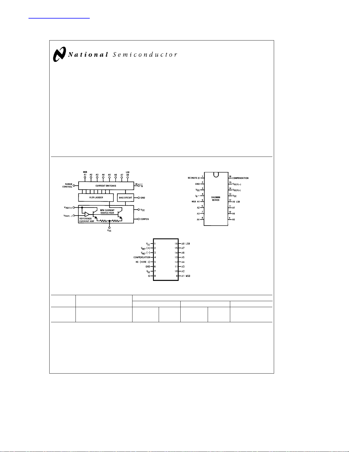
Block and Connection Diagrams
TL/H/5687– 1
Ordering Information
ACCURACY
7-bit 0
6-bit 0
*Note. Devices may be ordered by using either order number.
OPERATING TEMPERATURE ORDER NUMBERS
RANGE J PACKAGE (J16A)* N PACKAGE (N16A)* SO PACKAGE (M16A)
s
a
CsT
§
CsT
§
75§C DAC0807LCJ MC1408L7 DAC0807LCN MC1408P7 DAC0807LCM
A
s
a
75§C DAC0806LCJ MC1408L6 DAC0806LCN MC1408P6 DAC0806LCM
A
Dual-In-Line Package
Order Number
DAC0808, DAC0807,
or DAC0806
See NS Package
Number J16A,
M16A or N16A
TL/H/5687– 2
Small-Outline Package
TL/H/5687– 13
Top View
DAC0808LCN MC1408P8 DAC0808LCM
C
1995 National Semiconductor Corporation RRD-B30M115/Printed in U. S. A.
TL/H/5687
Absolute Maximum Ratings (Note 1)
If Military/Aerospace specified devices are required,
please contact the National Semiconductor Sales
Office/Distributors for availability and specifications.
Power Supply Voltage
V
CC
V
EE
Digital Input Voltage, V5–V12
Applied Output Voltage, V
Reference Current, I
O
14
b
10 VDCtoa18 V
b
11 VDCtoa18 V
Reference Amplifier Inputs, V14, V15 V
a
18 V
b
18 V
CC,VEE
DC
DC
DC
DC
5mA
Power Dissipation (Note 3) 1000 mW
Storage Temperature Range
Lead Temp. (Soldering, 10 seconds)
Dual-In-Line Package (Plastic) 260
Dual-In-Line Package (Ceramic) 300
Surface Mount Package
Vapor Phase (60 seconds) 215
Infrared (15 seconds) 220
Operating Ratings
Temperature Range T
DAC0808LC Series 0sT
ESD Susceptibility (Note 4) TBD
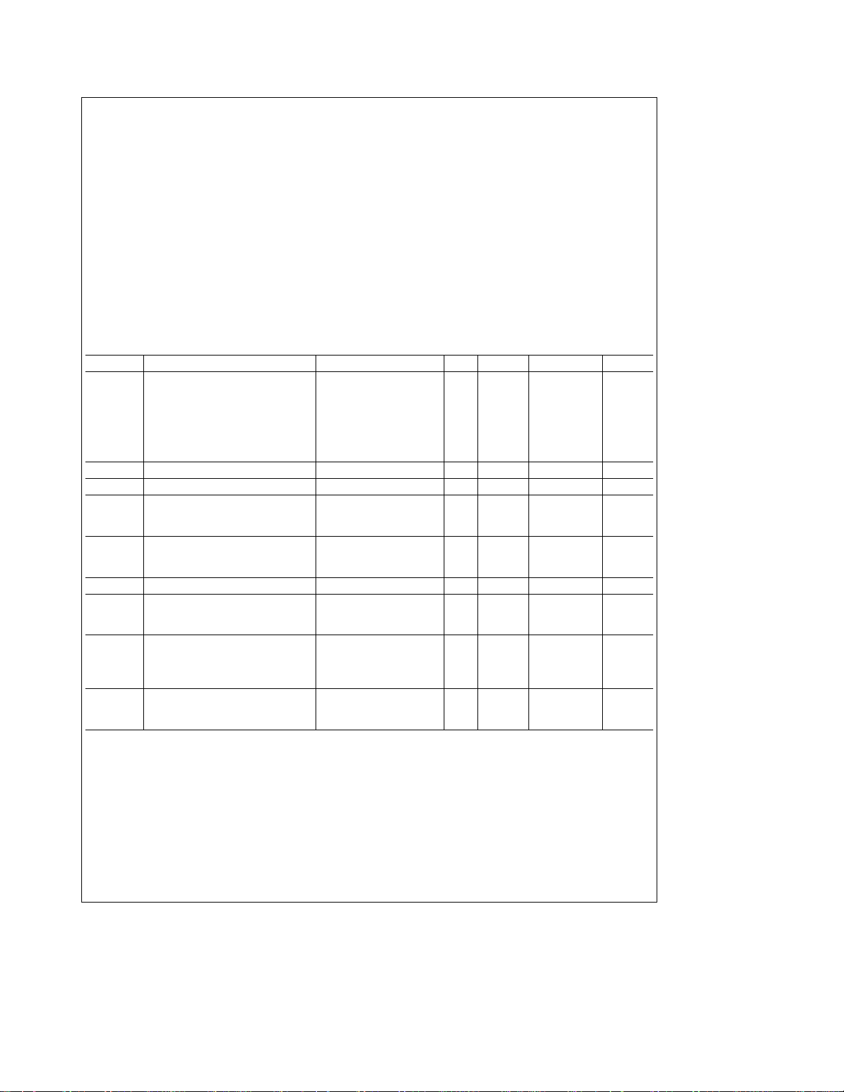
Electrical Characteristics
e
(V
CC
e
0§Ctoa75§C, and all digital inputs at high logic level unless otherwise noted.)
5V, V
EE
eb
15 VDC,V
/R14e2 mA, DAC0808: T
REF
eb
55§Ctoa125§C, DAC0808C, DAC0807C, DAC0806C, T
A
Symbol Parameter Conditions Min Typ Max Units
E
r
Relative Accuracy (Error Relative
to Full Scale I
DAC0808LC (LM1408-8)
)
O
(Figure 4)
DAC0807LC (LM1408-7), (Note 5)
DAC0806LC (LM1408-6), (Note 5)
e
Settling Time to Within (/2 LSB T
t
PLH,tPHL
TCI
O
(Includes t
Propagation Delay Time T
Output Full Scale Current Drift
PLH
)
MSB Digital Input Logic Levels
V
IH
V
IL
High Level, Logic ‘‘1’’ 2 V
Low Level, Logic ‘‘0’’ 0.8 V
MSB Digital Input Current
High Level V
Low Level V
I
15
Reference Input Bias Current
Output Current Range
I
O
Output Current V
Output Current, All Bits Low
Output Voltage Compliance (Note 2) E
eb
V
EE
VEEBelowb10V
5V, I
REF
e
1mA
25§C (Note 6), 150 ns
A
(Figure 5)
e
25§C,
A
(Figure 5)
30 100 ns
g
20 ppm/§C
(Figure 3)
(Figure 3)
e
5V 0 0.040 mA
IH
e
0.8V
IL
(Figure 3)
b
0.003
b
1
(Figure 3)
eb
V
5V 0 2.0 2.1 mA
EE
eb
V
EE
e
REF
R14e1000X,
(Figure 3)
(Figure 3)
s
0.19%, T
r
15V, T
2.000V,
e
25§C 0 2.0 4.2 mA
A
1.9 1.99 2.1 mA
04mA
e
25§C
A
b
65§Ctoa150§C
s
T
MIN
A
g
0.19 %
g
0.39 %
g
0.78 %
b
0.8 mA
b
3 mA
b
0.55,a0.4 V
b
5.0,a0.4 V
s
T
A
s
a
75§C
MAX
%
DC
DC
DC
DC
C
§
C
§
C
§
C
§
A
2
Electrical Characteristics (Continued)
e
(V
CC
e
0§Ctoa75§C, and all digital inputs at high logic level unless otherwise noted.)
5V, V
EE
eb
15 VDC,V
/R14e2 mA, DAC0808: T
REF
eb
55§Ctoa125§C, DAC0808C, DAC0807C, DAC0806C, T
A
Symbol Parameter Conditions Min Typ Max Units
SRI
REF
Reference Current Slew Rate
Output Current Power Supply
Sensitivity
Power Supply Current (All Bits
(Figure 6)
b
5VsV
(Figure 3)
4 8 mA/ms
s
b
16.5V 0.05 2.7 mA/V
EE
Low)
I
CC
I
EE
Power Supply Voltage Range T
V
CC
V
EE
e
25§C,
A
(Figure 3)
4.5 5.0 5.5 V
b
4.5
2.3 22 mA
b
4.3
b
15
b
13 mA
b
16.5 V
DC
DC
Power Dissipation
All Bits Low V
All Bits High V
Note 1: Absolute Maximum Ratings indicate limits beyond which damage to the device may occur. DC and AC electrical specifications do not apply when operating
the device beyond its specified operating conditions.
Note 2: Range control is not required.
Note 3: The maximum power dissipation must be derated at elevated temperatures and is dictated by T
allowable power dissipation at any temperature is P
device, T
line N package, this number increases to 175
Note 4: Human body model, 100 pF discharged through a 1.5 kX resistor.
Note 5: All current switches are tested to guarantee at least 50% of rated current.
Note 6: All bits switched.
Note 7: Pin-out numbers for the DAL080X represent the dual-in-line package. The small outline package pinout differs from the dual-in-line package.
e
125§C, and the typical junction-to-ambient thermal resistance of the dual-in-line J package when the board mounted is 100§C/W. For the dual-in-
JMAX
e
(T
D
C/W and for the small outline M package this number is 100§C/W.
§
e
CC
e
V
CC
e
CC
e
V
CC
b
TA)/iJAor the number given in the Absolute Maixmum Ratings, whichever is lower. For this
JMAX
5V, V
5V, V
15V, V
15V, V
eb
5V 33 170 mW
EE
eb
15V 106 305 mW
EE
eb
5V 90 mW
EE
eb
15V 160 mW
EE
, iJA, and the ambient temperature, TA. The maximum
JMAX
A
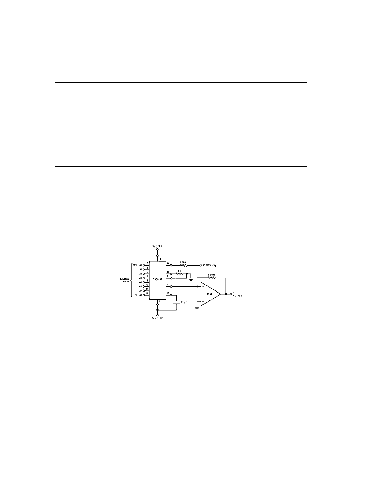
Typical Application
A1
10V
A2
a
a
...
2
4
#
e
V
O
FIGURE 1.a10V Output Digital to Analog Converter (Note 7)
3
A8
256
J
TL/H/5687– 3
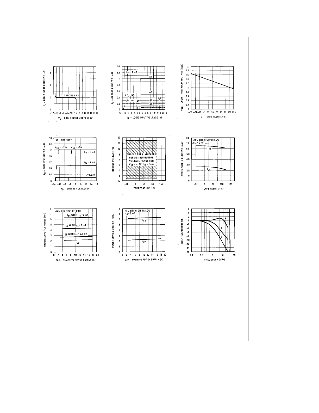
Typical Performance Characteristics
e
V
CC
5V, V
EE
eb
15V, T
e
25§C, unless otherwise noted
A
Logic Input Current vs
Input Voltage Bit Transfer Characteristics
Output Current vs Output
Voltage (Output Voltage
Compliance)
Output Voltage Compliance
vs Temperature
Logic Threshold Voltage vs
Temperature
Typical Power Supply
Current vs Temperature
Typical Power Supply
Current vs V
EE
Typical Power Supply
Current vs V
CC
4
Reference Input
Frequency Response
TL/H/5687– 5
Unless otherwise specified: R14
R15e1kX,Ce15 pF, pin 16 to
e
V
EE;RL
Curve A: Large Signal Bandwidth
Method of
offset 1 V above ground.
Curve B: Small Signal Bandwidth
Method of
e
50X, pin 4 to ground.
,R
,V
L
REF
e
250X,V
e
2 Vp-p
REF
Figure 7
Figure 7
50 mVp-p offset 200 mV above
ground.
Curve C: Large and Small Signal
Bandwidth Method of
e
amp, R
2V, V
50X), R
L
e
100 mVp-p centered at 0V.
S
Figure 9
e
S
50X,V
(no op
REF
e
e
 Loading...