查询DAC0800供应商
DAC0800/DAC0802
8-Bit Digital-to-Analog Converters
General Description
The DAC0800 series are monolithic 8-bit high-speed
current-output digital-to-analog converters (DAC) featuring
typical settling times of 100 ns. When used as a multiplying
DAC, monotonic performance over a 40 to 1 reference current range is possible. The DAC0800 series also features
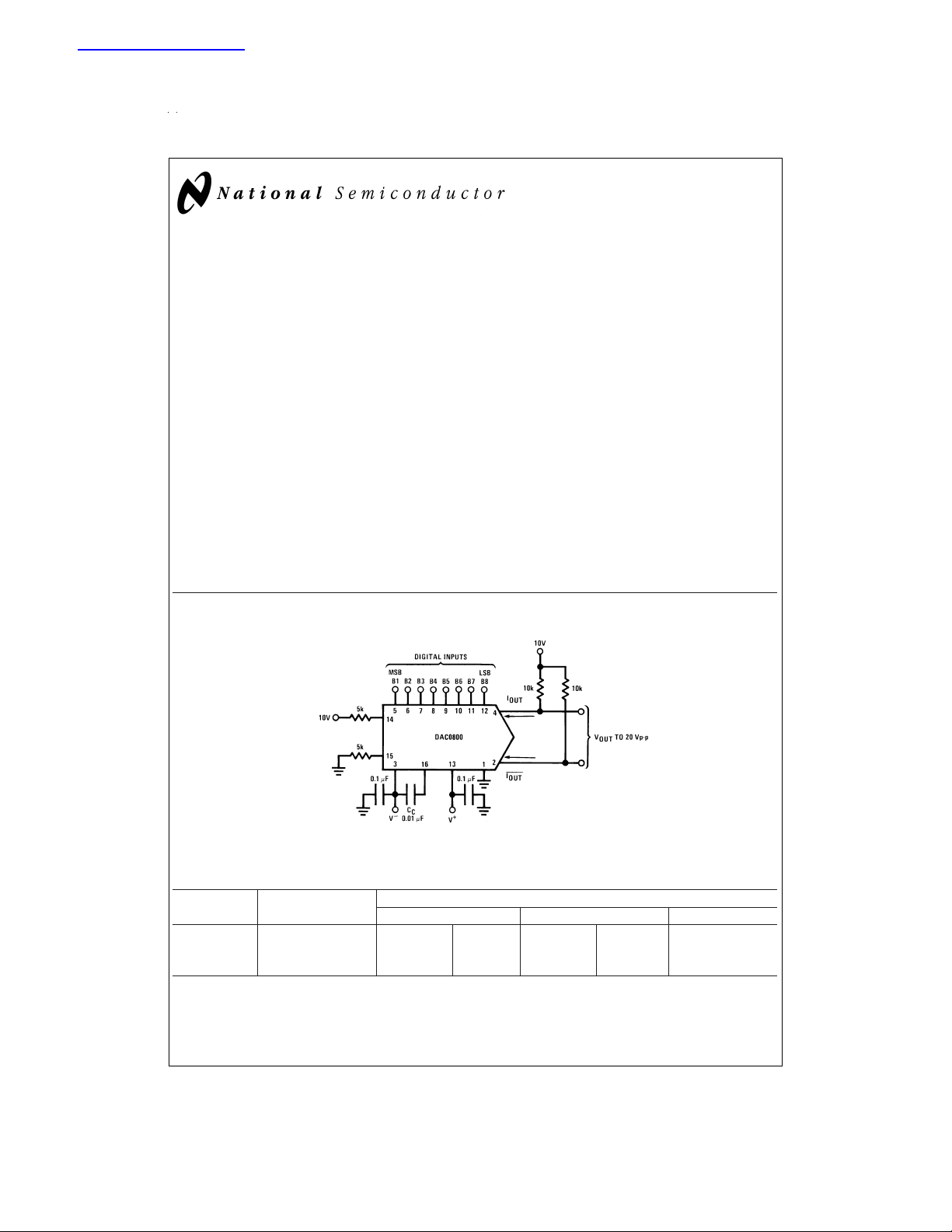
high compliance complementary current outputs to allow differential output voltagesof20Vp-p with simple resistor loads
as shown in
matching of better than
full-scale trims in most applications while the nonlinearities
of better than
ror accumulations.
The noise immune inputs of the DAC0800 series will accept
TTL levels with the logic threshold pin, V
Changing the V
logic families. The performance and characteristics of the
device are essentially unchanged over the full
±
18V power supply range; power dissipation is only 33 mW
±
with
5V supplies and is independent of the logic input
states.
Figure 1
. The reference-to-full-scale current
±
1 LSB eliminates the need for
±
0.1%over temperature minimizes system er-
, grounded.
potential will allow direct interface to other
LC
LC
±
4.5V to
June 1999
The DAC0800, DAC0802, DAC0800C and DAC0802C are a
direct replacement for the DAC-08, DAC-08A, DAC-08C,
and DAC-08H, respectively.
Features
n Fast settling output current: 100 ns
n Full scale error:
n Nonlinearity over temperature:
n Full scale current drift:
n High output compliance: −10V to +18V
n Complementary current outputs
n Interface directly with TTL, CMOS, PMOS and others
n 2 quadrant wide range multiplying capability
n Wide power supply range:
n Low power consumption: 33 mW at
n Low cost
±
1 LSB
±
10 ppm/˚C
±
4.5V to±18V
±
%
0.1
±
5V
DAC0800/DAC0802 8-Bit Digital-to-Analog Converters
Typical Applications
DS005686-1
FIGURE 1.±20 V
Output Digital-to-Analog Converter (Note 5)
P-P
Ordering Information
Non-Linearity Temperature Order Numbers
Range J Package (J16A) (Note 1) N Package (N16E) (Note 1) SO Package (M16A)
±
0.1%FS 0˚C ≤ TA≤ +70˚C DAC0802LCJ DAC-08HQ DAC0802LCN DAC-08HP DAC0802LCM
±
0.19%FS −55˚C ≤ TA≤ +125˚C DAC0800LJ DAC-08Q
±
0.19%FS 0˚C ≤ TA≤ +70˚C DAC0800LCJ DAC-08EQ DAC0800LCN DAC-08EP DAC0800LCM
Note 1: Devices may be ordered by using either order number.
© 1999 National Semiconductor Corporation DS005686 www.national.com

Absolute Maximum Ratings (Note 2)
If Military/Aerospace specified devices are required,
please contact the National Semiconductor Sales Office/
Distributors for availability and specifications.
Supply Voltage (V
+−V−
)
Power Dissipation (Note 3) 500 mW
Reference Input Differential Voltage
(V14 to V15) V
Reference Input Common-Mode
Range (V14, V15) V
Reference Input Current 5 mA
Logic Inputs V
Analog Current Outputs
−=−15V) 4.25 mA
(V
S
ESD Susceptibility (Note 4) TBD V
±
18V or 36V
−
−
−
to V−plus 36V
to V
to V
Storage Temperature −65˚C to +150˚C
Lead Temp. (Soldering, 10 seconds)
Dual-In-Line Package (plastic) 260˚C
Dual-In-Line Package (ceramic) 300˚C
Surface Mount Package
Vapor Phase (60 seconds) 215˚C
Infrared (15 seconds) 220˚C
+
Operating Conditions (Note 2)
+
Temperature (T
)
A
DAC0800L −55 +125 ˚C
DAC0800LC 0 +70 ˚C
DAC0802LC 0 +70 ˚C
Min Max Units
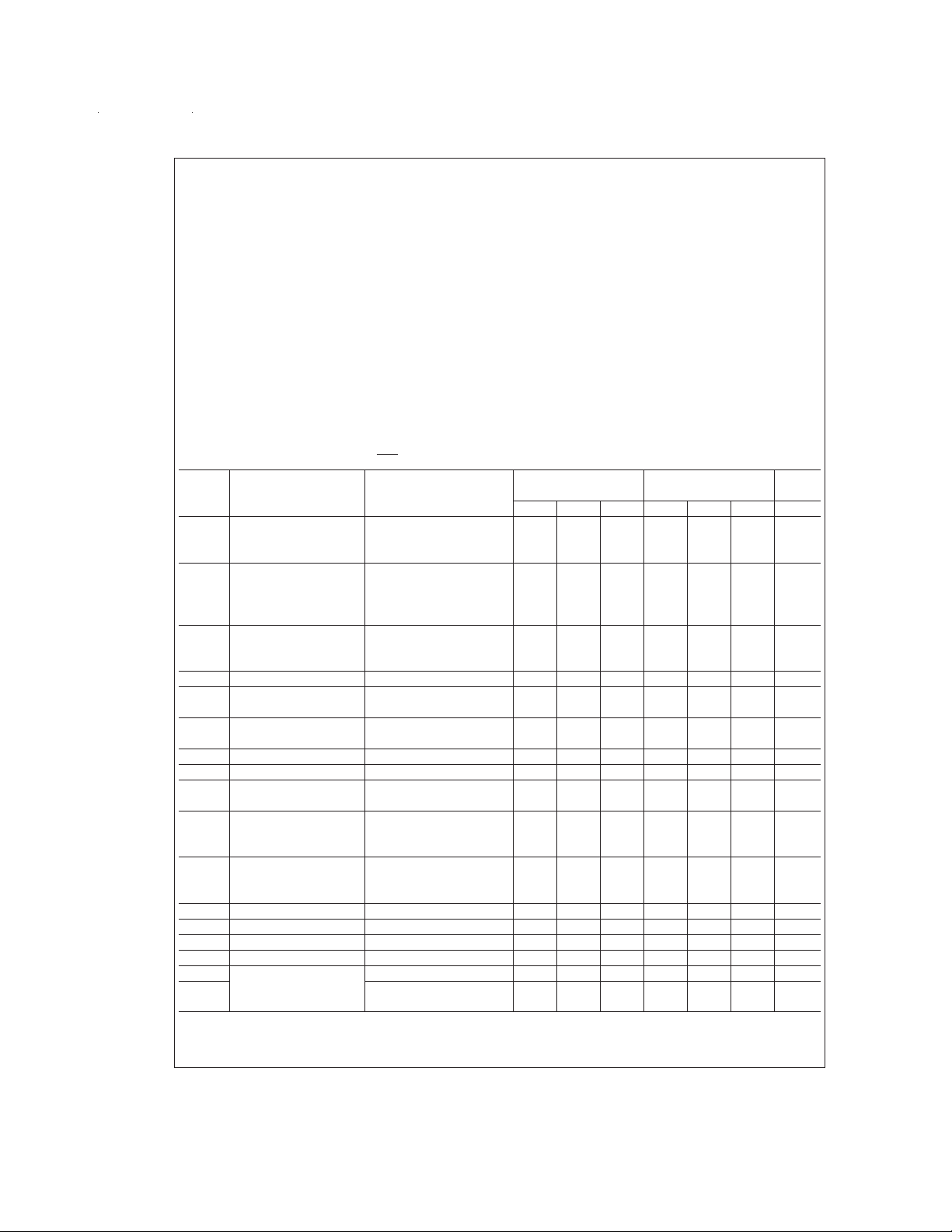
Electrical Characteristics
=
The following specifications apply for V
characteristics refer to both I
Symbol Parameter Conditions DAC0800LC Units
Resolution 888888Bits
Monotonicity 888888Bits
Nonlinearity
t
s
tPLH, Propagation Delay T
TCI
V
I
FS4
I
FSS
I
ZS
I
FSR
V
V
I
IL
I
IH
V
V
I
15
dl/dt Reference Input Slew Rate (
PSSI
PSSI
Settling Time To
tPHL Each Bit 35 60 35 60 ns
OC
IL
IH
IS
THR
All Bits Switched 35 60 35 60 ns
Full Scale Tempco
FS
Output Voltage Compliance Full Scale Current Change −10 18 −10 18 V
Full Scale Current V
Full Scale Symmetry I
Zero Scale Current 0.1 1.0 0.2 2.0 µA
Output Current Range V
Logic Input Levels
Logic “0” V
Logic “1” 2.0 2.0 V
Logic Input Current V
Logic “0” −10V≤VIN≤+0.8V −2.0 −10 −2.0 −10 µA
Logic “1” 2V≤VIN≤+18V 0.002 10 0.002 10 µA
Logic Input Swing V
Logic Threshold Range V
Reference Bias Current −1.0 −3.0 −1.0 −3.0 µA
Power Supply Sensitivity 4.5V≤V+≤18V 0.0001 0.01 0.0001 0.01
FS+
FS−
OUT
and I
±
15V, I
S
.
OUT
1
±
⁄2LSB, All Bits Switched 100 135 ns
“ON” or “OFF”, T
DAC0800L 100 135 ns
DAC0800LC 100 150 ns
=
25˚C
A
1
<
⁄2LSB, R
=
10.000V, R14=5.000 kΩ 1.984 1.992 2.000 1.94 1.99 2.04 mA
REF
R15=5.000 kΩ,T
FS4−IFS2
−
=
−5V 0 2.0 2.1 0 2.0 2.1 mA
−
=
−8V to −18V 0 2.0 4.2 0 2.0 4.2 mA
V
=
0V 0.8 0.8 V
LC
=
0V
LC
−
=
−15V −10 18 −10 18 V
=
±
15V −10 13.5 −10 13.5 V
S
Figure 11
−4.5V≤V−≤18V 0.0001 0.01 0.0001 0.01
=
1mA
I
REF
=
2 mA and T
REF
=
25˚C
A
>
20 MΩ Typ
OUT
=
25˚C
A
) 4.0 8.0 4.0 8.0 mA/µs
≤ TA≤ T
MIN
DAC0802LC DAC0800L/
Min Typ Max Min Typ Max
unless otherwise specified. Output
MAX
±
0.1
±
±
10
50
±
0.5±4.0
±
10
±
1
±
0.19%FS
±
±
50 ppm/˚C
8.0 µA
%/%
%/%
www.national.com 2

Electrical Characteristics (Continued)
=
The following specifications apply for V
characteristics refer to both I
OUT
and I
OUT
±
15V, I
S
.
Symbol Parameter Conditions DAC0800LC Units
=
±
Power Supply Current V
5V, I
S
I+ 2.3 3.8 2.3 3.8 mA
I− −4.3 −5.8 −4.3 −5.8 mA
=
5V, −15V, I
V
S
I+ 2.4 3.8 2.4 3.8 mA
I− −6.4 −7.8 −6.4 −7.8 mA
=
±
15V, I
V
S
I+ 2.5 3.8 2.5 3.8 mA
I− −6.5 −7.8 −6.5 −7.8 mA
=
D
Power Dissipation
P
±
5V, I
REF
5V,−15V, I
±
15V, I
REF
Note 2: Absolute Maximum Ratings indicate limits beyond which damage to the device may occur. DC and AC electrical specifications do not apply when operating
the device beyond its specified operating conditions.
Note 3: The maximum junction temperature of the DAC0800 and DAC0802 is 125˚C. For operating at elevated temperatures, devices in the Dual-In-Line J package
must be derated based on a thermal resistance of 100˚C/W,junction-to-ambient, 175˚C/W for the molded Dual-In-Line N package and 100˚C/W for the Small Outline
M package.
Note 4: Human body model, 100 pF discharged through a 1.5 kΩ resistor.
Note 5: Pin-out numbers for the DAC080X represent the Dual-In-Line package. The Small Outline package pin-out differs from the Dual-In-Line package.
REF
=
2 mA and T
MIN
≤ TA≤ T
unless otherwise specified. Output
MAX
DAC0802LC DAC0800L/
Min Typ Max Min Typ Max
=
1mA
REF
=
2mA
REF
=
2mA
REF
1mA 3348 3348mW
=
2 mA 108 136 108 136 mW
REF
=
2 mA 135 174 135 174 mW
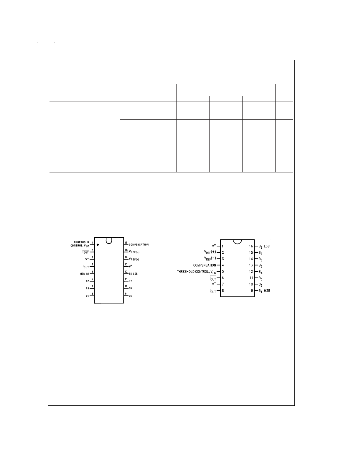
Connection Diagrams
Dual-In-Line Package
Top View
DS005686-13
See Ordering Information
Small Outline Package
DS005686-14
Top View
www.national.com3

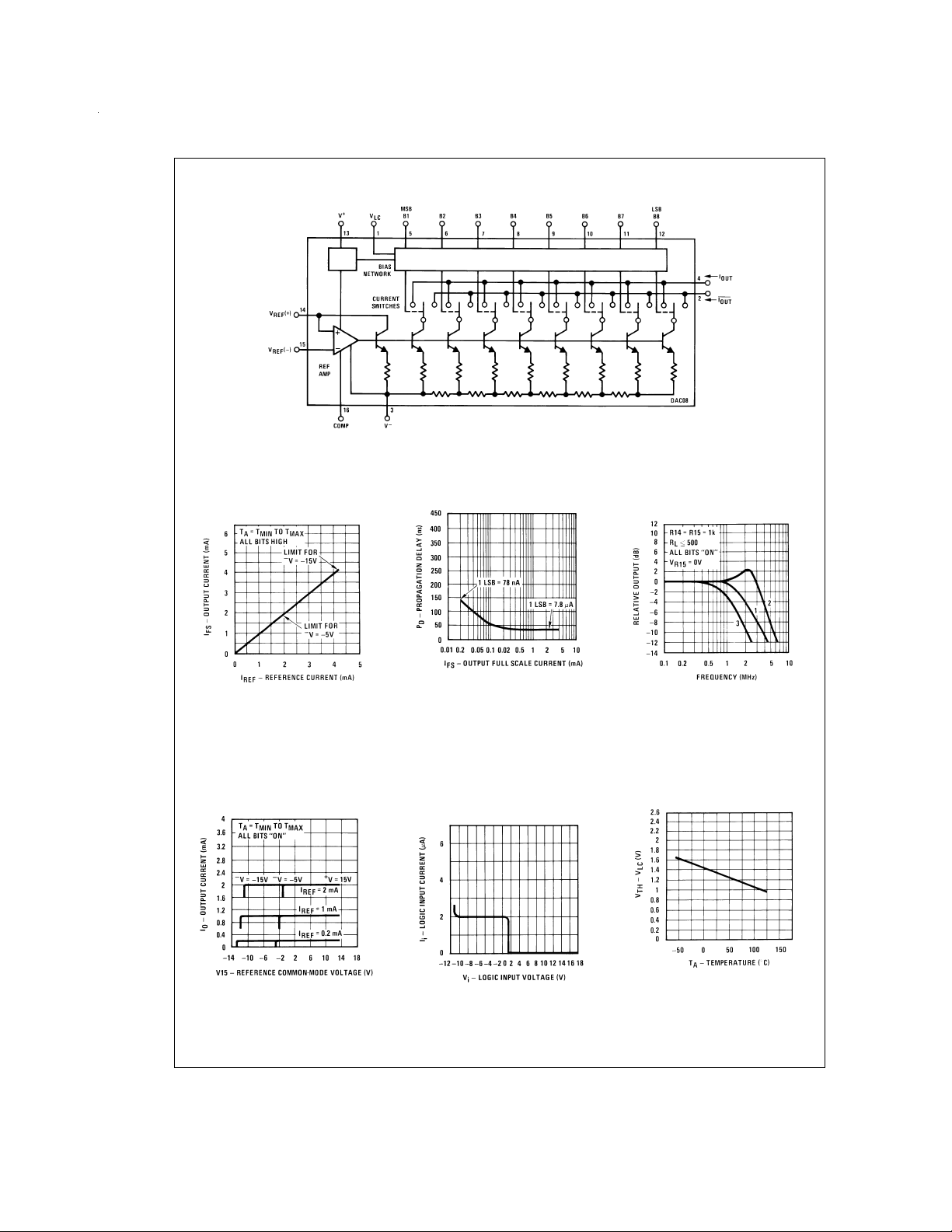
Block Diagram (Note 5)
Typical Performance Characteristics
DS005686-2
Full Scale Current
vs Reference Current
Reference Amp
Common-Mode Range
DS005686-22
LSB Propagation Delay vs I
Logic Input Current
vs Input Voltage
FS
DS005686-23
Reference Input
Frequency Response
Curve 1: C
Curve 2: C
200 mV.
Curve 3: C
0V and applied through 50Ω connected to pin
14.2V applied to R14.
=
C
=
C
=
C
15 pF, V
15 pF, V
0pF,V
IN
IN
=
IN
DS005686-24
=
2 Vp-p centered at 1V.
=
50 mVp-p centered at
100 mVp-p centered at
VTH—VLCvs Temperature
Note. Positive common-mode range is always
(V+) − 1.5V.
DS005686-25
www.national.com 4
DS005686-27
DS005686-26

Typical Performance Characteristics (Continued)
Output Current vs Output
Voltage (Output Voltage
Compliance)
Power Supply Current
vs +V
DS005686-28
Output Voltage Compliance
vs Temperature
Power Supply Current
vs −V
DS005686-29
Bit Transfer
Characteristics
LC
DS005686-30
=
0V).
Note. B1–B8 have identical transfer
characteristics. Bits are fully switched with less
than1⁄2LSB error, at less than±100 mV from
actual threshold. These switching points are
guaranteed to lie between 0.8 and 2V over the
operating temperature range (V
Power Supply Current
vs Temperature
Equivalent Circuit
DS005686-31
FIGURE 2.
DS005686-32
DS005686-33
DS005686-15
www.national.com5

Typical Applications
=
IO+I
For fixed reference, TTL operation, typical values are:
V
R
R15 ≈ R
C
V
REF
REF
C
LC
=
=
for all logic states
I
O
FS
=
10.000V
=
5.000k
REF
0.01 µF
0V (Ground)
FIGURE 3. Basic Positive Reference Operation (Note 5)
DS005686-5
DS005686-16
DS005686-21
FIGURE 4. Recommended Full Scale Adjustment
Circuit (Note 5)
B1 B2 B3 B4 B5 B6 B7 B8 IOmA IOmA E
Full Scale 111111111.992 0.000 −9.960 0.000
Full Scale−LSB 11111110 1.984 0.008 −9.920 −0.040
Half Scale+LSB 10000001 1.008 0.984 −5.040 −4.920
Half Scale 10000000 1.000 0.992 −5.000 −4.960
Half Scale−LSB 01111111 0.992 1.000 −4.960 −5.000
Zero Scale+LSB 00000001 0.008 1.984 −0.040 −9.920
Zero Scale 00000000 0.000 1.992 0.000 −9.960
FIGURE 6. Basic Unipolar Negative Operation (Note 5)
www.national.com 6
Note. R
sets IFS; R15 is for bias current cancellation
REF
FIGURE 5. Basic Negative Reference Operation
(Note 5)
DS005686-17
E
O
O

Typical Applications (Continued)
Pos. Full Scale 11111111−9.920 +10.000
Pos. Full Scale−LSB 11111110−9.840 +9.920
Zero Scale+LSB 10000001−0.080 +0.160
Zero Scale 10000000 0.000 +0.080
Zero Scale−LSB 01111111+0.080 0.000
Neg. Full Scale+LSB 00000001+9.920 −9.840
Neg. Full Scale 00000000+10.000 −9.920
FIGURE 7. Basic Bipolar Output Operation (Note 5)
DS005686-6
B1 B2 B3 B4 B5 B6 B7 B8 E
E
O
O
=
If R
within±0.05%, output is symmetrical about ground
R
L
L
B1 B2 B3 B4 B5 B6 B7 B8 E
DS005686-18
O
Pos. Full Scale 11111111+9.960
Pos. Full Scale−LSB 11111110+9.880
(+)Zero Scale 10000000+0.040
(−)Zero Scale 01111111−0.040
Neg. Full Scale+LSB 00000001−9.880
Neg. Full Scale 00000000−9.960
FIGURE 8. Symmetrical Offset Binary Operation (Note 5)
For complementary output (operation as negative logic DAC), connect inverting input of op amp to IO(pin 2), connect IO(pin 4) to ground.
DS005686-19
FIGURE 9. Positive Low Impedance Output Operation (Note 5)
www.national.com7

Typical Applications (Continued)
For complementary output (operation as a negative logic DAC) connect non-inverting input of op am to IO(pin 2); connect IO(pin 4) to ground.
DS005686-20
FIGURE 10. Negative Low Impedance Output Operation (Note 5)
Typical values: R
=
=
5k,+V
IN
10V
IN
DS005686-10
FIGURE 11. Pulsed Reference Operation (Note 5)
=
V
+ 1.4V
V
TH
LC
15V CMOS, HTL, HNIL
=
7.6V
V
TH
Note. Do not exceed negative logic input range of DAC.
FIGURE 12. Interfacing with Various Logic Families
DS005686-9
DS005686-11
(a) I
≥ peak negative swing of I
REF
IN
FIGURE 13. Accommodating Bipolar References (Note 5)
www.national.com 8
(b) +V
must be above peak positive swing of V
REF
DS005686-12
IN

Typical Applications (Continued)
FIGURE 14. Settling Time Measurement (Note 5)
DS005686-7
Note. For 1 µs conversion time with 8-bit resolution and 7-bit accuracy, an LM361 comparator replaces the LM319 and the reference current is doubled by
reducing R1, R2 and R3 to 2.5 kΩ and R4 to 2 MΩ.
DS005686-8
FIGURE 15. A Complete 2 µs Conversion Time, 8-Bit A/D Converter (Note 5)
www.national.com9

Physical Dimensions inches (millimeters) unless otherwise noted
Molded Small Outline Package (SO)
Order Numbers DAC0800LCM,
or DAC0802LCM
NS Package Number M16A
Molded Small Outline Package (SO)
Order Numbers DAC0800LCM,
or DAC0802LCM
NS Package Number M16A
www.national.com 10

Physical Dimensions inches (millimeters) unless otherwise noted (Continued)
Molded Dual-In-Line Package
Order Numbers DAC0800, DAC0802
NS Package Number N16E
DAC0800/DAC0802 8-Bit Digital-to-Analog Converters
LIFE SUPPORT POLICY
NATIONAL’S PRODUCTS ARE NOT AUTHORIZED FOR USE AS CRITICAL COMPONENTS IN LIFE SUPPORT
DEVICES OR SYSTEMS WITHOUT THE EXPRESS WRITTEN APPROVAL OF THE PRESIDENT AND GENERAL
COUNSEL OF NATIONAL SEMICONDUCTOR CORPORATION. As used herein:
1. Life support devices or systems are devices or
systems which, (a) are intended for surgical implant
into the body, or (b) support or sustain life, and
whose failure to perform when properly used in
accordance with instructions for use provided in the
2. A critical component is any component of a life
support device or system whose failure to perform
can be reasonably expected to cause the failure of
the life support device or system, or to affect its
safety or effectiveness.
labeling, can be reasonably expected to result in a
significant injury to the user.
National Semiconductor
Corporation
Americas
Tel: 1-800-272-9959
Fax: 1-800-737-7018
Email: support@nsc.com
www.national.com
National does not assume any responsibility for use of any circuitry described, no circuit patent licenses are implied and National reserves the right at any time without notice to change said circuitry and specifications.
National Semiconductor
Europe
Fax: +49 (0) 1 80-530 85 86
Email: europe.support@nsc.com
Deutsch Tel: +49 (0) 1 80-530 85 85
English Tel: +49 (0) 1 80-532 78 32
Français Tel: +49 (0) 1 80-532 93 58
Italiano Tel: +49 (0) 1 80-534 16 80
National Semiconductor
Asia Pacific Customer
Response Group
Tel: 65-2544466
Fax: 65-2504466
Email: sea.support@nsc.com
National Semiconductor
Japan Ltd.
Tel: 81-3-5639-7560
Fax: 81-3-5639-7507
 Loading...