

CR16HCS5/CR16HCS9/CR16MAR5/CR16MAS5
CR16MAS9/CR16MBR5/CR16MCS5/CR16MCS9
Family of 16-bit CAN-enabled CompactRISC
Microcontrollers
1.0 General Description
The family of 16-bit CompactRISC™ microcontroller is
based on a Reduced Instruction Set Computer (RISC) architecture. The device operates as a complete microcomputer with all system timing, interrupt logic, flash program
memory or ROM memory, RAM, EEPROM data memory,
and I/O ports included on-chip. It is ideally suited to a wide
range of embedded controller applications because of its
high performance, on-chip integrated features and low
power consumption resulting in decreased system cost.
The device offers the high performance of a RISC architecture while retaining the advantages of a traditional Com-
plex Instruction Set Computer (CISC): compact code, onchip memory and I/O, and reduced cost. The CPU uses a
three-stage instruction pipeline that allows execution of up
to one instruction per clock cycle, or up to 25 million instructions per second (MIPS) at a clock rate of 24 MHz.
The device contains a FullCAN class, CAN serial interface
for low/high speed applications with 15 orthogonal message buffers, each supporting standard as well as extended message identifiers.
January 2002
CR16HCS5/CR16HCS9/CR16MAR5/CR16MAS5 CR16MAS9/CR16MBR5/CR16MCS5/CR16MCS9 Family of 16-bit CAN-en-
abled CompactRISC Microcontrollers
Block Diagram
CR16B
RISC Core
Peripheral
Bus
Controller
64k-Byte
Flash
Program
Memory
Processing
Unit
Core Bus
3k-Byte
RAM
2176-Byte
EEPROM
Data
Memory
Peripheral Bus
Fast Clk
Clock Generator
Power-on-Reset
1.5k-Byte
ISP
Memory
Slow Clk*
Interrupt
Control
CR16CAN
FullCAN 2.0B
Power
Manage-
ment
Timing and
Watchdog
I/O
Please note that not all family members contain same peripheral modules and features.
TRI-STATE® is a registered trademark of National Semiconductor Corporation.
µWire/SPI
2x
USART
ACCESS
bus
4x
VTU
2x
MFT
12-ch
8-bit A/D
MIWU
2 Analog
Comparators

Table of Contents
1.0 General Description. . . . . . . . . . . . . . . . . . . . . . . . . . . . . . 1
2.0 Features . . . . . . . . . . . . . . . . . . . . . . . . . . . . . . . . . . . . . . . 3
3.0 Device Overview . . . . . . . . . . . . . . . . . . . . . . . . . . . . . . . . 5
3.1 CR16B CPU Core . . . . . . . . . . . . . . . . . . . . . . . . . . 5
3.2 Memory . . . . . . . . . . . . . . . . . . . . . . . . . . . . . . . . . .5
3.3 Input/Output Ports . . . . . . . . . . . . . . . . . . . . . . . . . . 5
3.4 Bus Interface Unit . . . . . . . . . . . . . . . . . . . . . . . . . .5
3.5 Interrupts . . . . . . . . . . . . . . . . . . . . . . . . . . . . . . . . . 5
3.6 Multi-Input Wake-up . . . . . . . . . . . . . . . . . . . . . . . . . 6
3.7 Dual Clock and Reset . . . . . . . . . . . . . . . . . . . . . . .6
3.8 Power Management . . . . . . . . . . . . . . . . . . . . . . . . . 6
3.9 Multi-Function Timer . . . . . . . . . . . . . . . . . . . . . . . .6
3.10 Versatile timer unit. . . . . . . . . . . . . . . . . . . . . . . . . .6
3.11 Real-Time TIMER and Watchdog . . . . . . . . . . . . . . 6
3.12 USART. . . . . . . . . . . . . . . . . . . . . . . . . . . . . . . . . . . 6
3.13 MICROWIRE/SPI . . . . . . . . . . . . . . . . . . . . . . . . . . . 6
3.14 CR16CAN . . . . . . . . . . . . . . . . . . . . . . . . . . . . . . . . 7
3.15 ACCESS.bus Interface . . . . . . . . . . . . . . . . . . . . . .7
3.16 A/D Converter . . . . . . . . . . . . . . . . . . . . . . . . . . . . . 7
3.17 Analog Comparators . . . . . . . . . . . . . . . . . . . . . . . .7
3.18 Development Support . . . . . . . . . . . . . . . . . . . . . . .7
4.0 Device Pinouts . . . . . . . . . . . . . . . . . . . . . . . . . . . . . . . . . . 8
4.1 Pin Description. . . . . . . . . . . . . . . . . . . . . . . . . . . .10
5.0 System Configuration . . . . . . . . . . . . . . . . . . . . . . . . . . . 12
5.1 ENV0 and ENV1 Pins . . . . . . . . . . . . . . . . . . . . . . 12
5.2 Module Configuration (MCFG) Register . . . . . . . .12
5.3 Module Status (MSTAT) Register . . . . . . . . . . . . . 12
6.0 Input/Output Ports . . . . . . . . . . . . . . . . . . . . . . . . . . . . . . 13
6.1 Port Registers . . . . . . . . . . . . . . . . . . . . . . . . . . . . 13
6.2 Open-Drain Operation . . . . . . . . . . . . . . . . . . . . . .14
7.0 CPU and Core Registers . . . . . . . . . . . . . . . . . . . . . . . . . 15
7.1 General-Purpose Registers. . . . . . . . . . . . . . . . . . 15
7.2 Dedicated Address Registers . . . . . . . . . . . . . . . .15
7.3 Processor Status Register. . . . . . . . . . . . . . . . . . . 15
7.4 Configuration Register. . . . . . . . . . . . . . . . . . . . . .16
7.5 Addressing Modes. . . . . . . . . . . . . . . . . . . . . . . . .16
7.6 Stacks . . . . . . . . . . . . . . . . . . . . . . . . . . . . . . . . . .16
7.7 Instruction Set . . . . . . . . . . . . . . . . . . . . . . . . . . . . 16
8.0 Bus Interface Unit . . . . . . . . . . . . . . . . . . . . . . . . . . . . . . 18
8.1 Bus Cycles. . . . . . . . . . . . . . . . . . . . . . . . . . . . . . . 18
8.2 BIU Control Registers . . . . . . . . . . . . . . . . . . . . . .18
8.3 Wait and Hold States Used . . . . . . . . . . . . . . . . . .20
9.0 Memory . . . . . . . . . . . . . . . . . . . . . . . . . . . . . . . . . . . . . . . 22
9.1 Flash EEPROM Program Memory. . . . . . . . . . . . .22
9.2 RAM Memory. . . . . . . . . . . . . . . . . . . . . . . . . . . . .25
9.3 Flash EEPROM Data Memory. . . . . . . . . . . . . . . .25
9.4 ISP Memory . . . . . . . . . . . . . . . . . . . . . . . . . . . . . . 27
10.0 Interrupts . . . . . . . . . . . . . . . . . . . . . . . . . . . . . . . . . . . . . 31
10.1 Interrupt Operation . . . . . . . . . . . . . . . . . . . . . . . . . 31
10.2 Non-Maskable Interrupt . . . . . . . . . . . . . . . . . . . . .32
10.3 Maskable Interrupts . . . . . . . . . . . . . . . . . . . . . . . .32
10.4 Interrupt Registers . . . . . . . . . . . . . . . . . . . . . . . . .33
10.5 Interrupt Programming Procedures . . . . . . . . . . . .35
11.0 Power Management . . . . . . . . . . . . . . . . . . . . . . . . . . . . . 36
11.1 Active Mode . . . . . . . . . . . . . . . . . . . . . . . . . . . . . .36
11.2 Power Save Mode . . . . . . . . . . . . . . . . . . . . . . . . .36
11.3 Idle Mode. . . . . . . . . . . . . . . . . . . . . . . . . . . . . . . . 36
11.4 Halt Mode . . . . . . . . . . . . . . . . . . . . . . . . . . . . . . . .36
11.5 Clock Inputs and Reset Configuration . . . . . . . . . .36
11.6 Switching Between Power Modes . . . . . . . . . . . . .36
12.0 Dual Clock and Reset . . . . . . . . . . . . . . . . . . . . . . . . . . . 39
12.1 External Crystal Network. . . . . . . . . . . . . . . . . . . . 39
12.2 Main System Clock . . . . . . . . . . . . . . . . . . . . . . . . 40
12.3 Slow System Clock . . . . . . . . . . . . . . . . . . . . . . . . 40
12.4 Power-On Reset . . . . . . . . . . . . . . . . . . . . . . . . . .41
12.5 External Reset. . . . . . . . . . . . . . . . . . . . . . . . . . . .41
12.6 Dual Clock and Reset Registers . . . . . . . . . . . . . .41
12.7 Slow Clock Prescaler Register (PRSSC). . . . . . . .41
12.8 Slow Clock Prescaler 1 Register (PRSSC1) . . . . .41
13.0 Multi-Input Wake-Up . . . . . . . . . . . . . . . . . . . . . . . . . . . .42
13.1 Wake-Up Edge Detection Register (WKEDG) . . . .42
13.2 Wake-Up Enable Register (WKENA). . . . . . . . . . .42
13.3 Wake-Up Interrupt Control Register 1 (WKCTRL1) 43
13.4 Wake-Up Interrupt Control Register 1 (WKCTRL2) 43
13.5 Wake-Up Pending Register (WKPND) . . . . . . . . . .43
13.6 Wake-Up Pending Clear Register (WKPCL) . . . . .43
13.7 Programming Procedures . . . . . . . . . . . . . . . . . . .44
14.0 Real-Time Timer and WATCHDOG . . . . . . . . . . . . . . . . .45
14.1 TWM Structure. . . . . . . . . . . . . . . . . . . . . . . . . . . .45
14.2 Timer T0 Operation . . . . . . . . . . . . . . . . . . . . . . . .45
14.3 WATCHDOG Operation . . . . . . . . . . . . . . . . . . . . .46
14.4 TWM Registers . . . . . . . . . . . . . . . . . . . . . . . . . . . .46
14.5 WATCHDOG Programming Procedure . . . . . . . . .47
15.0 Multi-Function Timer . . . . . . . . . . . . . . . . . . . . . . . . . . . .49
15.1 Timer Structure. . . . . . . . . . . . . . . . . . . . . . . . . . . .49
15.2 Timer Operating Modes . . . . . . . . . . . . . . . . . . . . .51
15.3 Timer Interrupts . . . . . . . . . . . . . . . . . . . . . . . . . . .54
15.4 Timer I/O Functions . . . . . . . . . . . . . . . . . . . . . . . .54
15.5 Timer Registers . . . . . . . . . . . . . . . . . . . . . . . . . . .56
16.0 Versatile-Timer-Unit (VTU) . . . . . . . . . . . . . . . . . . . . . . .58
16.1 VTU Functional Description . . . . . . . . . . . . . . . . . .58
16.2 VTU Registers . . . . . . . . . . . . . . . . . . . . . . . . . . . .61
17.0 MICROWIRE/SPI . . . . . . . . . . . . . . . . . . . . . . . . . . . . . . . .65
17.1 MICROWIRE Operation . . . . . . . . . . . . . . . . . . . . .65
17.2 Master Mode . . . . . . . . . . . . . . . . . . . . . . . . . . . . .66
17.3 Slave Mode . . . . . . . . . . . . . . . . . . . . . . . . . . . . . .67
17.4 Interrupt Generation. . . . . . . . . . . . . . . . . . . . . . . .68
17.5 MICROWIRE Interface Registers. . . . . . . . . . . . . .68
18.0 USART . . . . . . . . . . . . . . . . . . . . . . . . . . . . . . . . . . . . . . . .71
18.1 Functional Overview . . . . . . . . . . . . . . . . . . . . . . . .71
18.2 USART Operation . . . . . . . . . . . . . . . . . . . . . . . . .71
18.3 USART Registers . . . . . . . . . . . . . . . . . . . . . . . . . .75
18.4 Baud Rate Calculations . . . . . . . . . . . . . . . . . . . . .77
19.0 ACCESS.bus Interface . . . . . . . . . . . . . . . . . . . . . . . . . . .78
19.1 ACB Protocol Overview . . . . . . . . . . . . . . . . . . . . .78
19.2 ACB Functional Description . . . . . . . . . . . . . . . . . .79
19.3 ACB Registers . . . . . . . . . . . . . . . . . . . . . . . . . . . .82
19.4 Usage Hints . . . . . . . . . . . . . . . . . . . . . . . . . . . . . .84
20.0 CR16CAN Module. . . . . . . . . . . . . . . . . . . . . . . . . . . . . . .85
20.1 Functional Description . . . . . . . . . . . . . . . . . . . . . .85
20.2 Basic CAN Concepts . . . . . . . . . . . . . . . . . . . . . . .87
20.3 Message Transfer . . . . . . . . . . . . . . . . . . . . . . . . .95
20.4 Acceptance Filtering . . . . . . . . . . . . . . . . . . . . . . . .96
20.5 Receive Structure . . . . . . . . . . . . . . . . . . . . . . . . . .97
20.6 Transmit Structure . . . . . . . . . . . . . . . . . . . . . . . . 100
20.7 Interrupts . . . . . . . . . . . . . . . . . . . . . . . . . . . . . . . 103
20.8 Time Stamp Counter . . . . . . . . . . . . . . . . . . . . . . 105
20.9 Memory Organization. . . . . . . . . . . . . . . . . . . . . .105
20.10 System Start-Up and Multi-Input Wake-Up . . . . .116
21.0 Analog Comparators . . . . . . . . . . . . . . . . . . . . . . . . . . . 118
21.1 Analog Comparator Control/Status Register
(CMPCTRL). . . . . . . . . . . . . . . . . . . . . . . . . . . . . . 118
21.2 Analog Comparator Usage . . . . . . . . . . . . . . . . . .118
22.0 A/D Converter . . . . . . . . . . . . . . . . . . . . . . . . . . . . . . . . .119
22.1 Operating Modes . . . . . . . . . . . . . . . . . . . . . . . . . 119
22.2 A/D Converter Registers . . . . . . . . . . . . . . . . . . .120
22.3 A/D Converter Programming . . . . . . . . . . . . . . . .122
23.0 Memory Map . . . . . . . . . . . . . . . . . . . . . . . . . . . . . . . . . .123
24.0 Register Layouts . . . . . . . . . . . . . . . . . . . . . . . . . . . . . .129
24.1 Register layout . . . . . . . . . . . . . . . . . . . . . . . . . . . 129
25.0 ELECTRICAL AND THERMAL CHARACTERISTICS . . 136
26.0 Appendix . . . . . . . . . . . . . . . . . . . . . . . . . . . . . . . . . . . . .152
26.1 CR16CAN. . . . . . . . . . . . . . . . . . . . . . . . . . . . . . . 152
26.2 8/16-bit microwire/spi (MWSPI16) . . . . . . . . . . . .154
26.3 Timing and watchdog module . . . . . . . . . . . . . . . 154
www.national.com 2

1.0 General Description (Continued)
The device has up to 64K bytes of reprogrammable flash EEPROM program memory or ROM memory, 1.5K bytes of
flash EEPROM In-System-Programming memory, 3K bytes
of static RAM, 2K bytes of non-volatile EEPROM data memory and 128 bytes with high endurance, two USARTs, two 16bit multi-function timers, one SPI/MICROWIRE-PLUS™ serial interface, a 12-channel A/D converter, two analog comparators, WATCHDOG™ protection mechanism, and up to 56
general-purpose I/O pins.
The device operates with a high-frequency crystal as the
main clock source and either the prescaled main clock
source or with a low frequency (32.768 kHz) oscillator in
Power Save mode. The device supports several Power Save
modes which are combined with multi-source interrupt and
wake-up capabilities.
This device also has a Versatile Timer Unit (VTU) with four
timer sub-systems, a CAN interface, and ACCESS.bus synchronous serial bus interface.
Powerful cross-development tools are available from National Semiconductor and third party suppliers to support the development and debugging of application software for the
device. These tools let you program the application software
in C and are designed to take full advantage of the CompactRISC architecture.
In the following text, device is always referred to the family of
16-bit CAN-enabled CompactRISC Microtroller.
— FullCAN interface with 15 message buffers complaint
to CAN specification 2.0B active
— Versatile Timer Unit with four subsystems (VTU)
— Two analog comparators
— Integrated WATCHDOG logic
• I/O Features
— Up to 56 general-purpose I/O pins (shared with on-chip
peripheral I/O pins)
— Programmable I/O pin characteristics: TRI-STATE out-
put, push-pull output, weak pull-up input, high-impedance input
— Schmitt triggers on general purpose inputs
• Power Supply
— 4.5V to 5.5V single-supply operation
• Temperature Range
— –40°C to +85°C
— –40°C to +125°C
• Development Support
— Real-time emulation and full program debug capabili-
ties available
— CompactRISC tools provide C programming and de-
bugging support
2.0 Features
• CPU Features
— Fully static core, capable of operating at any rate from
0 to 24 MHz (4 MHz minimum in active mode)
— 50 ns instruction cycle time with a 20 MHz external
clock frequency
— Multi-source vectored interrupts (internal, external,
and on-chip peripheral)
— Dual clock and reset
• On-chip power-on reset
• On-Chip Memory
— Up to 64K bytes flash EEPROM program memory; can
be programmed, erased, and reprogrammed by soft-
ware (100K cycles)
— 3K bytes of static RAM data memory
— For flash program memory devices, 1.5k bytes flash
EEPROM memory is available to store boot loader
code (100K cycles)
— 2K bytes of non-volatile EEPROM data memory with
low endurance (25K cycles) and 128 bytes with high
endurance (100K cycles)
• On-Chip Peripherals
— Two Universal Synchronous/Asynchronous Receiver/
Transmitter (USART) devices
— Programmable Idle Timer and real-time clock (T0)
— Two dual 16-bit multi-function timers (MFT1 and MFT2)
— 8/16-bit SPI/MICROWIRE-PLUS serial interface
— 12-channel, 8-bit Analog-to-Digital (A/D) converter
with external voltage reference, programmable sam-
ple-and-hold delay, and programmable conversion fre-
quency
— ACCESS.bus synchronous serial bus
3 www.national.com

CR16 CompactRISC Microcontroller with CAN Interface Family Selection Guide
Programmable devices
EEPROM
NSID
Speed
(MHz)
Flash/
(kByte)
Data
Memory
SRAM
(kBytes)
USART Timer I/Os
(Bytes)
Temp.
Range
Peripherals
Package
Type
CR16MCS9VJEx 16 64 2176 3 2
CR16MAS9VJEx 24 64 3 2
Factory Programmed devices
EEPROM
NSID
Speed
(MHz)
Flash/
(KByte)
Data
Memory
SRAM
(kBytes)
USART Timer I/Os
(Bytes)
CR16MCS9VJExy 16 64 2176 3 2
CR16MCS9VJExy 24 64 2176 3 2
ROM devices
EEPROM
Data
Memory
(Bytes)
SRAM
(kBytes)
USART Timer I/Os
NSID
Speed
(MHz)
Flash/
ROM
(KByte)
CR16HCS9VJEx 24 64 2176 3 2
CR16MCS5VJEx 24 64 2176 3 2
CR16MBR5VJEx 24 32 2176 3 2
CR16MAR5VJEx 24 32 3 2
CR16MAS5VJEx 24 64 3 2
Note:
• Suffix x in the NSID is defined below:
Temperature Ranges:
I = Industrial
E = Extended
• Suffix y in the NSID defines the ROM code.
Note: All devices contains Access.bus (ACB), Clock and Reset, MICROWIRE/API, Multi-Input Wake-Up (MIWU), Power
Management (PMM), and the Real-Time Timer and Watchdog (TWM) modules. Access.bus is compatible with I2C bus
offered by Philips Semiconductor.
-40°C to +85°C is represented when x is 8
-40°C to +125°C is represented when x is 7
CR16 CompactRISC Microcontroller with CAN Interface
Family Devices
National Semiconductor currently offers a variety of the
CR16 CompactRISC Microcontrollers with CAN interface.
The CR16MCS offer complete functionality in an 80-pin
PQFP package.
2MFT,
VTU
2MFT,
VTU
2MFT,
VTU
2MFT,
VTU
2MFT,
VTU
2MFT,
VTU
2MFT,
VTU
2MFT,
VTU
2MFT,
VTU
56 E, I
56 E, I
Temp.
Range
56 E, I
56 E, I
Temp.
Range
56 E, I
56 E, I
56 E, I
ADC, CAN,
Comparators
ADC, CAN,
Comparators
Peripherals
ADC, CAN,
Comparators
ADC, CAN,
Comparators
Peripherals
ADC, CAN,
Comparators
ADC, CAN,
Comparators
ADC, CAN,
Comparators
80 PQFP
80 PQFP
Package
Type
80 PQFP
80 PQFP
Package
Type
80 PQFP
80 PQFP
80 PQFP
56 E, I CAN, 80 PQFP
56 E, I CAN, 80 PQFP
www.national.com 4

3.0 Device Overview
The devices are complete microcomputers with all system
timing, interrupt logic, program memory, data memory, and I/
O ports included on-chip, making it well-suited to a wide
range of embedded controller applications.
3.1 CR16B CPU CORE
The device uses a CR16B CPU core module. This is the
same core used in other CompactRISC family member designs, like DECT or GSM chipsets.
The high performance of the CPU core results from the implementation of a pipelined architecture with a two-bytes-percycle pipelined system bus. As a result, the CPU can support
a peak execution rate of one instruction per clock cycle.
Compared with conventional RISC processors, the device
differs in the following ways:
— The CPU core can use on-chip rather than external
memory. This eliminates the need for large and com-
plex bus interface units.
— Most instructions are 16 bits, so all basic instructions
are just two bytes long. Additional bytes are sometimes
required for immediate values, so instructions can be
two or four bytes long.
— Non-aligned word access is allowed. Each instruction
can operate on 8-bit or 16-bit data.
— The device is designed to operate with a clock rate in
the 10 to 24 MHz range rather than 100 MHz or more.
Most embedded systems face EMI and noise con-
straints that limit clock speed to these lower ranges. A
lower clock speed means a simpler, less costly silicon
implementation.
— The instruction pipeline uses three stages. A smaller
pipeline eliminates the need for costly branch predic-
tion mechanisms and bypass registers, while maintain-
ing adequate performance for typical embedded
controller applications.
For more information, please refer to the CR16B Programmer’s Reference Manual, Literature #: 633150.
3.2 MEMORY
The CompactRISC architecture supports a uniform linear address space of 2 megabytes. The device implementation of
this architecture uses only the lowest 128K bytes of address
space. Four types of on-chip memory occupy specific intervals within this address space:
• 64K bytes of flash EEPROM program memory (100K cycles)
• 48K bytes ROM programm memory version available also
(100K cycles)
• 3K bytes of static RAM
• 2K bytes of EEPROM data memory with low endurance
(25K cycles)
• 128 bytes with high endurance (100K cycles)
• 1.5K bytes flash EEPROM memory for ISP code
The 3K bytes of static RAM are used for temporary storage
of data and for the program stack and interrupt stack. Read
and write operations can be byte-wide or word-wide, depending on the instruction executed by the CPU. Each memory
access requires one clock cycle; no wait cycles or hold cycles
are required.
There are two types of flash EEPROM data memory storage.
The 2K bytes of EEPROM data memory with low endurance
(25K cycles) and 128 bytes of flash EEPROM data memory
with high endurance (100K cycles) are used for non-volatile
storage of data, such as configuration settings entered by the
end-user.
The 64K bytes of flash EEPROM program memory are used
to store the application program. It has security features to
prevent unintentional programming and to prevent unauthorized access to the program code. This memory can be programmed with a device external programming unit or with the
device installed in the application system (in-system programming).
There is a factory programmed boot memory used to store
In-System-Programming (ISP) code. (This code allows programming of the program memory via one of the USART interfaces in the final application.)
For flash EEPROM program and data memory, the device internally generates the necessary voltages for programming.
No additional power supply is required.
3.3 INPUT/OUTPUT PORTS
The device has 56 software-configurable I/O pins, organized
into seven 8-pin ports called Port B, Port C, Port F, Port G,
Port H, Port I, and Port L. Each pin can be configured to operate as a general-purpose input or general-purpose output.
In addition, many I/O pins can be configured to operate as a
designated input or output for an on-chip peripheral module
such as the USART, timer, A/D converter, or MICROWIRE/
SPI interface.
The I/O pin characteristics are fully programmable. Each pin
can be configured to operate as a TRI-STATE output, pushpull output, weak pull-up input, or high-impedance input.
3.4 BUS INTERFACE UNIT
The Bus Interface Unit (BIU) controls the interface between
the on-chip modules to the internal core bus. It determines
the configured parameters for bus access (such as the number of wait states for memory access) and issues the appropriate bus signals for each requested access.
The BIU uses a set of control registers to determine how
many wait states and hold states are to be used when accessing flash EEPROM program memory, ISP memory and
the I/O area (Port B and Port C). Upon start-up the configuration registers are set for slowest possible memory access.
To achieve fastest possible program execution, appropriate
values should be programmed. These settings vary with the
clock frequency and the type of on-chip device being accessed.
5 www.national.com

3.5 INTERRUPTS
The Interrupt Control Unit (ICU31L) receives interrupt requests from internal and external sources and generates interrupts to the CPU. An interrupt is an event that temporarily
stops the normal flow of program execution and causes a
separate interrupt service routine to be executed. After the interrupt is serviced, CPU execution continues with the next instruction in the program following the point of interruption.
Interrupts from the timers, USARTs, MICROWIRE/SPI interface, multi-input wake-up, and A/D converter are all
maskable interrupts; they can be enabled or disabled by the
software. There are 32 of these maskable interrupts, organized into 32 predetermined levels of priority.
The highest-priority interrupt is the Non-Maskable Interrupt
(NMI), which is generated by a signal received on the NMI input pin.
3.6 MULTI-INPUT WAKE-UP
The Multi-Input Wake-Up (MIWU16) module can be used for
either of two purposes: to provide inputs for waking up (exiting) from the HALT, IDLE, or Power Save mode; or to provide
general-purpose edge-triggered maskable interrupts from
external sources. This 16-channel module generates four
programmable interrupts to the CPU based on the signals received on its 16 input channels. Channels can be individually
enabled or disabled, and programmed to respond to positive
or negative edges.
3.7 DUAL CLOCK AND RESET
The Dual Clock and Reset (CLK2RES) module generates a
high-speed main system clock from an external crystal network. It also provides the main system reset signal and a
power-on reset function.
This module also generates a slow system clock (32.768
kHz) from another external crystal network. The slow clock is
used for operating the device in power-save mode. Without a
32.768kHz external crystal network, the low speed system
clock can be derived from the high speed clock by a prescaler.
Also, two independent clocks divided down from the high
speed clock are available on output pins.
3.8 POWER MANAGEMENT
The Power Management Module (PMM) improves the efficiency of the device by changing the operating mode and
therefore the power consumption according to the required
level of activity.
The device can operate in any of four power modes:
— Active: The device operates at full speed using the
high-frequency clock. All device functions are fully operational.
— Power Save: The device operates at reduced speed
using the slow clock. The CPU and some modules can
continue to operate at this low speed.
— IDLE: The device is inactive except for the Power Man-
agement Module and Timing and Watchdog Module,
which continue to operate using the slow clock.
— HALT: The device is inactive but still retains its internal
state (RAM and register contents).
3.9 MULTI-FUNCTION TIMER
The Multi-Function Timer (MFT16) module contains two independent timer/counter units called MFT1 and MFT2, each
containing a pair of 16-bit timer/counter registers. Each timer/
counter unit can be configured to operate in any of the following modes:
— Processor-Independent Pulse Width Modulation
(PWM) mode, which generates pulses of a specified
width and duty cycle, and which also provides a general-purpose timer/counter.
— Dual Input Capture mode, which measures the
elapsed time between occurrences of external events,
and which also provides a general-purpose timer/
counter.
— Dual Independent Timer mode, which generates sys-
tem timing signals or counts occurrences of external
events.
— Single Input Capture and Single Timer mode, which
provides one external event counter and one system
timer.
3.10 VERSATILE TIMER UNIT
The Versatile Timer Unit (VTU) module contains four independent timer subsystems, each operating in either dual 8-bit
PWM configuration, as a single 16-bit PWM timer, or a 16-bit
counter with two input capture channels. Each of the four timer subsystems offer an 8-bit clock prescaler to accommodate
a wide range of frequencies.
3.11 REAL-TIME TIMER AND WATCHDOG
The Timing and Watchdog Module (TWM) generates the
clocks and interrupts used for timing periodic functions in the
system. It also provides Watchdog protection against software errors. The module operates on the slow system clock.
The real-time timer can generate a periodic interrupt to the
CPU at a software-programmed interval. This can be used
for real-time functions such as a time-of-day clock. The realtime timer can trigger a wake-up condition from power-save
mode via the Multi-Input Wake-Up module.
The Watchdog is designed to detect program execution errors such as an infinite loop or a “runaway” program. Once
Watchdog operation is initiated, the application program
must periodically write a specific value to a Watchdog register, within specific time intervals. If the software fails to do so,
a Watchdog error is triggered, which resets the device.
3.12 USART
The USART supports a wide range of programmable baud
rates and data formats, and handles parity generation and
several error detection schemes. The baud rate is generated
on-chip, under software control.
There are two independent USARTs in the device and they
offer a wake-up condition from the power-save mode via the
Multi-Input Wake-Up module.
3.13 MICROWIRE/SPI
The MICROWIRE/SPI (MWSPI) interface module supports
synchronous serial communications with other devices that
conform to MICROWIRE or Serial Peripheral Interface (SPI)
specifications. It supports 8-bit and 16-bit data transfers.
www.national.com 6

The MICROWIRE interface allows several devices to communicate over a single system consisting of four wires: serial
in, serial out, shift clock, and slave enable. At any given time,
the MICROWIRE interface operates as the master or a slave.
The support supports the full set of slave select for multislave implementation.
In master mode, the shift clock is generated on chip under
software control. In slave mode, a wake-up out of powersave mode is triggered via the Multi-Input Wake-Up module.
3.14 CR16CAN
The CR16CAN device contains a FullCAN class, CAN serial
bus interface for applications that require a high speed (up to
1MBits per second) or a low speed interface with CAN bus
master capability. The data transfer between CAN and the
CPU is established by 15 memory mapped message buffers,
which can be individually configured as receive or transmit
buffers. An incoming message is filtered by two masks, one
for the first 14 message buffers and another one for the 15th
message buffer to provide a basic CAN path. A priority decoder allows any buffer to have the highest or lowest transmit
priority. Remote transmission requests can be processed automatically by automatic reconfiguration to a receiver after
transmission or by automated transmit scheduling upon reception. In addition, a time stamp counter (16-bits wide) is
provided to support real time applications.
The CR16CAN device is a fast core bus peripheral, which allows single cycle byte or word read/write access. A set of diagnostic features (such as loopback, listen only, and error
identification) support the development with the CR16CAN
module and provide a sophisticated error management tool.
The CR16CAN receiver can trigger a wake-up condition out
of the power-save modes via the Multi-Input Wake-Up module.
3.17 ANALOG COMPARATORS
The Dual Analog Comparator (ACMP2) module contains two
independent analog comparators with all necessary control
logic. Each comparator unit compares the analog input voltages applied to two input pins and determines which voltage
is higher. The CPU uses a memory-mapped register to control the comparator and to obtain the comparison results. The
comparison result can also be applied to comparator output
pins.
3.18 DEVELOPMENT SUPPORT
A powerful cross-development tool set is available from National Semiconductor and third parties to support the development and debugging of application software for the
CR16MCS9. The tool set lets you program the application
software in C and is designed to take full advantage of the
CompactRISC architecture.
There are In-System Emulation (ISE) devices available for
the device from iSYSTEM™, as well as lower-cost evaluation
boards. See your National Semiconductor sales representative for current information on availability and features of emulation equipment and evaluation boards.
3.15 ACCESS.BUS INTERFACE
The ACCESS.bus interface module (ACB) is a two-wire serial interface with the ACCESS.bus physical layer. It is also
compatible with Intel’s System Management Bus (SMBus)
and Philips’ I2C bus. The ACB module can be configured as
a bus master or slave, and can maintain bi-directional communications with both multiple master and slave devices.
The ACCESS.bus receiver can trigger a wake-up condition
out of the power-save modes via the Multi-Input Wake-Up
module.
3.16 A/D CONVERTER
The A/D Converter (ADC) module is a 12-channel multiplexed-input analog-to-digital converter. The A/D Converter
receives an analog voltage signal on an input pin and converts the analog signal into an 8-bit digital value using successive approximation. The CPU can then read the result
from a memory-mapped register. The module supports four
automated operating modes, providing single-channel or 4channel operation in single or continuous mode.
The device has a separate pin, Vref, for the A/D reference
voltage.
7 www.national.com

4.0 Device Pinouts
Pin Name Alternate Function(s) Pin Number Type
PH4 MWCS 1 I/O
PH5 MD1D0 2 I/O
PH6 MD0D1 3 I/O
PH7 MSK 4 I/O
PB0 D0 5 I/O
PB1 D1 6 I/O
PB2 D2 7 I/O
PB3 D3 8 I/O
PB4 D4 9 I/O
PB5 D5 10 I/O
PB6 D6 11 I/O
PB7 D7 12 I/O
ENV0/CLKOUT1 13 I/O
SDA 14 I/O
SCL 15 I/O
GND 16 PWR
Vcc 17 PWR
GND 18 PWR
CANTx 19 O
CANRx 20 I
PC0 D8 21 I/O
PC1 D9 22 I/O
PC2 D10 23 I/O
PC3 D11 24 I/O
PC4 D12 25 I/O
PC5 D13 26 I/O
PC6 D14 27 I/O
PC7 D15 28 I/O
PG7 CKX1 29 I/O
PG6 TDX1 30 I/O
PG5 RDX1 31 I/O
PG4 TIO6 32 I/O
PG3 TIO5 33 I/O
PG2 CKX2 34 I/O
PG1 TDX2 35 I/O
PG0 RDX2 36 I/O
CLKOUT2 37 O
ENV1/CLK
PF7 TIO4 38 I/O
PF6 TIO3 39 I/O
PF5 T2B 40 I/O
PF4 T2A 41 I/O
PF3 TIO2 42 I/O
PF2 TIO1 43 I/O
PF1 TIB 44 I/O
Table 1Package Pin Assignments
1
37 I/O
www.national.com 8

Table 1Package Pin Assignments
Pin Name Alternate Function(s) Pin Number Type
PF0 TIA 45 I/O
NMI 46 I
X1CKO 47 O
X1CKI 48 I
GND 49 PWR
Vcc 50 PWR
GND 51 PWR
X2CKO 52 O
X2CKI 53 I
2
RESET
PI0 ACH0
PI1 ACH1
PI2 ACN2
PI3 ACH3
PI4 ACH4
PI5 ACH5
PI6 ACH6
PI7 ACH7
3
3
3
3
3
3
3
3
54 I
55 I/O
56 I/O
57 I/O
58 I/O
59 I/O
60 I/O
61 I/O
62 I/O
Vref 63 PWR
AGND 64 PWR
AVcc 65 PWR
PH0 ACH83, WUI4 66 I/O
PH1 ACH93, WUI5 67 I/O
PH2 ACH103, WUI6 68 I/O
PH3 ACH113, WUI7 69 I/O
GND 70 PWR
Vcc 71 PWR
GND 72 PWR
PL0 COMP1N3, WUI0 73 I/O
PL1 COMP1P3, WUI1 74 I/O
PL2 COMP1O, WUI2 75 I/O
PL3 COMP2O, WUI3 76 I/O
PL4 COMP2P
PL5 COMP2N
3
3
77 I/O
78 I/O
PL6 TIO7 79 I/O
PL7 TIO8 80 I/O
Note 1: The ENV0 and ENV1 pins each have a weak pull-up to keep the input from floating.
Note 2: The RESET input has a weak pulldown.
Note 3: These functions are always enabled, due to the direct low-impedance path to these pins.
9 www.national.com

4.1 PIN DESCRIPTION
The following is a brief description of all device pins.
Some pins have alternate functions which may be enabled.
These pins can be individually configured as general purpose pins, even when the module they belong to is enabled.
Table 2Input Pins
Signal Type Active Pin (* for a shared pin) Function
X1CKI OSC High Main oscillator clock input.
X2CKI OSC High 32kHz oscillator clock input.
RESET CMOS Low Chip general reset pin. Schmitt trigger input, asynchronous.
ISE CMOS Low Interrupt input for development system.
T1B CMOS Prog. * Timer 1 input B. Shares pin with I/O port pin PF1.
T2B CMOS Prog. * Timer 2 input B. Shares pin with I/O port pin PF5.
RDX1 CMOS High * USART 1 receive data input. Shares pin with I/O port pin PG5.
RDX2 CMOS High * USART 2 receive data input. Shares pin with I/O port pin PG0.
ACH0 Analog * A2D converter channel 0. Shares pin with I/O port pin PI0
ACH1 Analog * A2D converter channel 1. Shares pin with I/O port pin PI1
ACH2 Analog * A2D converter channel 2. Shares pin with I/O port pin PI2
ACH3 Analog * A2D converter channel 3. Shares pin with I/O port pin PI3
ACH4 Analog * A2D converter channel 4. Shares pin with I/O port pin PI4
ACH5 Analog * A2D converter channel 5. Shares pin with I/O port pin PI5
ACH6 Analog * A2D converter channel 6. Shares pin with I/O port pin PI6
ACH7 Analog * A2D converter channel 7. Shares pin with I/O port pin PI7
ACH8 Analog * A2D converter channel 8. Shares pin with I/O port pin PH0
ACH9 Analog * A2D converter channel 9. Shares pin with I/O port pin PH1
ACH10 Analog * A2D converter channel 10. Shares pin with I/O port pin PH2
ACH11 Analog * A2D converter channel 11. Shares pin with I/O port pin PH3
MWCS CMOS Low * SPI/MICROWIRE slave select. Shares pin with I/O port pin PH4.
NMI CMOS Low External non-maskable interrupt.
ENV0 CMOS Low * Strap to select operating environment.
ENV1 CMOS Low * Strap pin to select operating environment.
ENV2 CMOS Low Strap pin to select operating environment.
CANRx CMOS High CAN receive data input.
Table 3Output Pins
Signal Type Active
Pin (* for
a shared pin)
Function
X1CKO OSC High Main oscillator clock output.
X2CKO OSC High 32kHz oscillator clock output.
CLK CMOS High * External reference clock for development environment (shared with ENV1).
CLKOUT1CMOS High * Clock output generated through prescaler (shared with ENV0).
CLKOUT2CMOS High * Clock output generated through prescaler (shared with ENV1).
www.national.com 10
Table 3Output Pins
Signal Type Active
TDX1 CMOS High * USART 1 transmit data output (shared with PG6).
TDX2 CMOS High * USART 2 transmit data output (shared with PG1).
CANTx CMOS High CAN output.
Signal Type Active
PF[0:7] CMOS High * Generic I/O port. Shared with T1A, T1B, TIO1, TIO2, T2A, T2B, TIO3, TIO4.
PG[0:7] CMOS High * Generic I/O port. Shared with RDX2, TDX2, CKX2, TIO5, TIO6, RDX1, TDX1,
PB[0:7] CMOS High * Generic I/O port.
PC[0:7] CMOS High * Generic I/O port.
PL[0:7] CMOS High * Generic I/O port. Shared with 6 comparator pins, MIWU16 on PL0:3.
PH[0:7] CMOS High * Generic I/O port. Shared with ADC input channels 8-11, MWCS, MDIDO,
PI[0:7] CMOS High * Generic I/O port. Shared with ADC input channels 0-7.
T1A CMOS Prog * Timer 1 input A. Shared with I/O port pin PF0.
Pin (* for
a shared pin)
Pin (* for a
shared pin)
Function
Table 4Input/Output Pins
Function
CKX1.
MDODI, MSK; MIWU16 on PH4:7.
T2A CMOS Prog * Timer 2 input A. Shared with I/O port pin PF4.
TIO[0:7] CMOS Prog * Versatile timer unit I/Os. Shared with PF2:3, PF6:7, PG3:4, PL6:7.
MDIDO CMOS High * Master In/Slave Out port: SPI/Microwire. Shared with I/O pin PH5,
MDODI CMOS High * Master Out/Slave In port: SPI/Microwire. Shared with I/O pin PH6.
MSK CMOS Prog * SPI/Microwire clock. Shared with I/O pin PH7.
CKX1 CMOS High * USART 1 clock. Shared with I/O pin PG7.
CKX2 CMOS High * USART 2 clock. Shared with I/O pin PG2
SCL CMOS High ACCESS.bus clock I/O.
SDA CMOS High ACCESS.bus data I/O.
Table 5Power Supply
Signal Function
Vcc Main digital power supply (4 total).
Vref Voltage reference supply for analog to digital converter.
AVcc Analog power supply for analog/digital converter.
AGND Analog reference ground supply.
GND Main digital reference ground (8 total).
11 www.national.com
5.0 System Configuration
The device has two input pins, ENV0 and ENV1, which are
used to specify the operating environment of the device upon
reset. There are also two system configuration registers,
called the Module Configuration (MCFG) register and the
Module Status (MSTAT) register.
5.1 ENV0 AND ENV1 PINS
Upon reset, the operating mode of the device is determined
by the state of the ENV0 and ENV1 input pins, as indicated
in Table6.
Table 6Operating Environment Selection
ENV1 ENV0 Operating Environment
0 0 Test Mode Flash Memory
0 1 Test Mode
1 0 In-System-Programming mode (ISP)
Internal ROM enabled Mode (IRE), if
1 1
program memory is not empty; or ISPMode, if program memory is empty
normal operating mode, the CLK pin operates
as a CPU clock output.
CLK1OE Generated Clock Output 1 Enable. When
cleared (0), the CLKOUT1 pin (ENV0) stays in
high impedance state. When set (1), the pin
outputs the clock from the prescaler controlled
by PRSSC1.SCDIV1.
CLK2OE Generated Clock Output 2 Enable. When this
bit is set (1) and CLKOE is cleared, the
CLKOUT2 pin (ENV1) outputs the clock from
the prescaler controlled by PRSSC1.SCDIV2.
Otherwise, the CLKOUT2 pin is in high impedance state.
5.3 MODULE STATUS (MSTAT) REGISTER
The MSTAT register is a byte-wide, read-only register that indicates the general status of the device.
The MCFG register format is shown below.
74 3 2 1 0
Reserved PGMBUSY Reserved OENV1 OENV0
In the case where the ENV1 and ENV0 pins are both high,
the reset algorithm looks at the FLCTRL2.EMPTY bit to determine whether the program memory is empty, and sets the
operating mode accordingly.
The ENV0 and ENV1 pins have on-chip pull-up devices that
are enabled during reset while the pins are being sampled.
Therefore, if they are left unconnected, the inputs are considered high and the normal operating mode (IRE-Mode) is selected and the CPU starts to execute code at address 0. To
enter any other operating mode, the external hardware must
drive the appropriate input low.
In the case where the ISP-Mode is selected, the chip starts
executing the ISP code residing in the on-chip ISP-Memory
area.
The test modes are Reserved for factory testing and for external programming of the flash EEPROM program memory.
They should not be invoked otherwise.
5.2 MODULE CONFIGURATION (MCFG)
REGISTER
The MCFG register is a byte-wide, read/write register that
sets the clock output features of the device.
Upon reset, the non-reserved bits of this register are cleared
to zero. The start-up software must write a specific value to
this register in order to configure the CLK output pin function.
When the software writes to this register, it must write a zero
to each reserved bit for the device to operate properly. The
register should be written in active mode only, not in power
save, HALT, or IDLE mode. However, the register contents
are preserved during all power modes.
The MCFG register format is shown below.
7 6 5 4 3 2 1 0
Reserved CLK2OE Reserved CLK1OE CLKOE Reserved
OENV(1:0) Operating Environment. These two bits contain
the values applied to the ENV1 and ENV0 pins
upon reset. These bit values are controlled by
the external hardware upon reset and are held
constant in the register until the next reset.
PGMBUSY Flash EEPROM Programming Busy. This bit is
automatically set to 1 when either the program
memory or the data memory is busy being programmed or erased. It is cleared to 0 when neither of the two flash EEPROM memories is
busy being programmed or erased. When this
bit is set, the software should not attempt any
write access to either of these two memories.
CLKOE CPU Clock Output Enable. When this bit is
cleared (0), the CLK pin (ENV1) remains in the
high-impedance state. When this bit is set (1) in
www.national.com 12
6.0 Input/Output Ports
Each device has up to 56 software-configurable I/O pins, organized into seven ports of up to eight pins per port. The
ports are named Port B, Port C, Port F, Port G, Port H, Port
I, and Port L.
Each pin can be configured to operate as a general-purpose
input or general-purpose output. In addition, many I/O pins
can be configured to operate as a designated input or output
for an on-chip peripheral module such as the USART or the
Multi-Input Wakeup. This is called the pin's “alternate function.” The alternate functions of all I/O pins are shown in the
pinout diagrams in Table1.
The I/O pin characteristics are fully programmable. Each pin
can be configured to operate as a TRI-STATE output, pushpull output, weak pull-up input, or high-impedance input. Different pins within the same port can be individually configured to operate in different modes.
Figure1 is a diagram showing the functional features of an I/
O port pin. The register bits, multiplexers, and buffers allow
the port pin to be configured into the various operating
modes.The output buffer is a TRI-STATE buffer with weak
pull-up capability. The weak pull-up, if used, prevents the port
pin from going to an undefined state when it operates as an
input.
The input buffer is disabled when it is not needed to prevent
leakage current caused by an input signal’s level between
Vcc-0.2 and Vss+0.2 [Volts]. When enabled, it buffers the input signal and sends the pin's logic level to the appropriate
on-chip module where it is latched. A Schmitt-Trigger minimizes the effects of electrical noise.
The electrical characteristics and drive capabilities of the input and output buffers are described in Section25.0.
For some pins, a direct low-impedance path is provided between the pin and an internal analog function. These are the
input pins to the A/D converter and the analog comparators.
6.1 PORT REGISTERS
Each port has an associated set of memory-mapped registers used for controlling the port and for holding the port data.
In general, there are five such registers:
— PxALT: Port alternate function register
— PxDIR: Port direction register
— PxDIN: Port data input register
— PxDOUT: Port data output register
— PxWKPU: Port weak pull-up register
In the descriptions of the ports and port registers, the lowercase letter “x” represents the port designation, either B, C, F,
G, H, I, or L. For example, “PxDIR register” means any one
of the port direction registers: PBDIR, PCDIR, PFDIR, and so
on.
All of the port registers are byte-wide read/write registers, except for the port data input registers, which are read-only registers. Each register bit controls the function of the
corresponding port pin. For example, PFDIR.2 (bit 2 of the
PFDIR register) controls the operation of port pin PF2.
Alternate Function
enable
Weak pull-up
Register
Alt Device Direction
Direction
Register
Alt Device Data Output
Data Out
Register
Data Input
Alternate Data Input
Data In Read Strobe
{
{
{
Weak pull-up
Direction
Data Out
Alt
Figure 1.I/O Pin Functional Diagram
MUX1
Alt
MUX2
Alt
*
1
MUX3
Alt
PIN
13 www.national.com

6.1.1 Port Alternate Function Register
Each port that supports an alternate function (any port other
than Port B or Port C) has an alternate function register (PxALT). This register determines whether the port pins are used
for general-purpose I/O or for the predetermined alternate
function. Each port pin can be controlled independently.
A bit cleared to 0 in the alternate function register causes the
corresponding pin to be used for general-purpose I/O. In this
configuration, the output buffer is controlled by the direction
register and the data output register. The input buffer is routed to the data input register. The input buffer is blocked except when the buffer is actually being read.
A bit set to 1 in the alternate function register causes the corresponding pin to be used for its predetermined peripheral I/
O function. The output buffer data and TRI-STATE configuration are controlled by signals coming from the on-chip peripheral device. The input buffer is enabled continuously in this
case. To minimize power consumption, the input signal
should be held within 0.2 volts of the VCC or GND voltage.
A reset operation clears the port alternate function registers
to 0, which programs the pins to operate as general-purpose
I/O ports. This register must be enabled before the corresponding alternate function is enabled.
6.1.2 Port Direction Register
The port direction register (PxDIR) determines whether each
port pin is used for input or for output. A bit cleared to 0 causes the pin to operate as an input, which puts the output buffer
in the high-impedance state. A bit set to 1 causes the pin to
operate as an output, which enables the output buffer.
A reset operation clears the port direction registers to 0,
which programs the pins to operate as inputs.
6.2 OPEN-DRAIN OPERATION
A port pin can be configured to operate as an inverting opendrain output buffer. To do this, the CPU should clear the bit in
the data output register (PxDOUT) and then use the port direction register (PxDIR) to set the value of the port pin. With
the direction register bit set to 1 (direction=out), the value
zero is forced on the pin. With the direction register bit
cleared to 0 (direction=in), the pin is placed in the TRI-STATE
mode. If desired, the internal weak pull-up can be enabled to
pull the signal high when the output buffer is in the TRISTATE mode.
6.1.3 Port Data Input Register
The data input register (PxDIN) is a read-only register that returns the current state of each port pin. The CPU can read
this register at any time even when the pin is configured as
an output.
6.1.4 Port Data Output Register
The data output register (PxDOUT) holds the data to be driven onto each port pin configured to operate as a general-purpose output. In this configuration, writing to the register
changes the output value. Reading the register returns the
last value written to the register.
A reset operation leaves the register contents unchanged.
Upon power-up, the registers contain unknown values.
6.1.5 Port Weak Pull-Up Register
The weak pull-up register (PxWKPU) determines whether
each port pin uses a weak pull-up on the output buffer. A bit
set to 1 causes the weak pull-up to be used, while a bit
cleared to 0 causes the causes the weak pull-up not to be
used.
The pull-up device, if enabled by the register bit, operates in
the general-purpose I/O mode whenever the port output buffer is in the TRI-STATE mode. In the alternate function mode,
the pull-ups are always disabled.
A reset operation clears the port weak pull-up registers to 0,
which disables all pull-ups.
www.national.com 14

7.0 CPU and Core Registers
The device uses the same CR16B CPU core as other CompactRISC family members. The core's Reduced Instruction
Set Computer (RISC) architecture allows a processing rate
of up to one instruction per clock cycle.
The CPU core uses a set of internal registers:
— General-purpose registers (R0-R13, RA, and SP)
— Dedicated address registers (PC, ISP, and INTBASE)
— Processor Status Register (PSR)
— Configuration Register (CFG)
All of these registers are 16 bits wide except for the three address registers, which are 21 bits wide.
Some register bits are designated as “reserved.” The CPU
must write a zero to each of these bit locations when it writes
to the register. Read operations from reserved bit locations
return undefined values.
7.1 GENERAL-PURPOSE REGISTERS
There are 16 general-purpose registers, designated R0
through R13, RA, and SP. Registers R0 through R13 can be
used for any purpose such as holding variables, addresses,
or index values. The RA register is usually used to store the
return address upon entry into a subroutine. The SP register
is usually used as the pointer to the program run-time stack.
If a general-purpose register is used for a byte-wide operation, only the low-order byte is referenced or modified. The
high-order byte is not used or affected by a byte-wide operation.
7.2 DEDICATED ADDRESS REGISTERS
There are three dedicated address registers: the Program
Counter (PC), the Interrupt Stack Pointer (ISP), and the Interrupt Base Register (INTBASE). Each of these registers is
21 bits wide.
7.2.1 Program Counter
The PC register contains the address of the least significant
word currently being fetched. It is automatically incremented
or changed by the appropriate amount each time an instruction is executed.
The least significant bit of the PC is always zero, thus instructions must always be aligned to an even address in the range
of 0000 to 1FFFE hex.
Upon reset, the PC register is initialized to zero and program
execution starts at that address (if in IRE-Mode). When a reset signal is received, bits 1 through 16 of the PC register
(prior to initialization) are stored in register R0. This allows
the software to determine the point in the program at which
the reset occurred.
7.2.2 Interrupt Stack Pointer
The ISP register points to the lowest address of the last item
stored on the interrupt stack. This stack is used by the hardware when an interrupt or trap service procedure is invoked.
7.2.3 Interrupt Base Register
The INTBASE register holds the address of the Dispatch Table for interrupts and traps. The least significant bit of the register is always zero. Thus, the Dispatch Table starts at an
even address in the range of 0000 to FFFE.
7.3 PROCESSOR STATUS REGISTER
The Processor Status Register (PSR) holds status information and selects the operating modes for the CPU core. The
format of the register is shown below.
15 14 13 12 11 10 9 8 7 6 5 4 3 2 1 0
Reserved I P E 0 N Z F 0 0 L T C
C bit The Carry (C) bit indicates whether a carry or
borrow occurred after addition or subtraction. It
is set to 1 if a carry or borrow occurred, or
cleared to 0 otherwise.
T bit The Trace (T) bit, when set, causes a Trace
(TRC) trap to be executed after every instruction. This bit is automatically cleared to 0 when
a trap or interrupt occurs.
L bit The Low (L) bit is set by comparison opera-
tions. In a comparison of unsigned integers, the
bit is set to 1 if the second operand (Rdest) is
less than the first operand (Rsrc). Otherwise, it
is cleared to 0.
F bit The Flag (F) bit is a general condition flag that
is set by various instructions. It may be used to
signal exception conditions or to distinguish the
results of an instruction. For example, integer
arithmetic instructions use this bit to indicate an
overflow condition after an addition or subtraction operation.
Z bit The Zero (Z) bit is set by comparison opera-
tions. In a comparison of integers, the bit is set
to 1 if the two operands are equal. Otherwise,
it is cleared to 0.
N bit The Negative (N) bit is set by comparison oper-
ations. In a comparison of signed integers, the
bit is set to 1 if the second operand (Rdest) is
less than the first operand (Rsrc). Otherwise, it
is cleared to 0.
E bit The Local Maskable Interrupt Enable (E) bit is
used to enable or disable maskable interrupts.
If this bit and the Global Maskable Interrupt Enable (I) bit are both set to 1, all maskable interrupts are accepted. Otherwise, only the nonmaskable interrupt is accepted. The E bit is set
to 1 by the Enable Interrupts (EI) instruction
and cleared to 0 by the Disable Interrupts (DI)
instruction.
P bit The Trace Trap Pending (P) bit is used togeth-
er with the Trace (T) bit to prevent a Trace
(TRC) trap from occurring more than once for
any instruction. The P bit may be cleared to 0
(no TRC trap pending) or set to 1 (TRC trap
pending).
15 www.national.com

I bit The Global Maskable Interrupt Enable (I) bit is
used to enable or disable maskable interrupts.
If this bit and the Local Maskable Interrupt Enable (E) bit are both set to 1, all maskable interrupts are accepted. Otherwise, only the nonmaskable interrupt is accepted. This bit is automatically cleared to 0 when an interrupt occurs
and automatically set to 1 upon completion of
an interrupt service routine.
Upon reset, all non-reserved bits of the register are cleared
to 0 except for the E bit (bit 9), which is set to 1. When a device reset occurs, the PSR contents prior to the reset are
stored into register R1, allowing the initialization software to
determine the state of the device prior to the reset operation.
7.4 CONFIGURATION REGISTER
The Configuration (CFG) register is a 16-bit core register that
determines the size of the INTBASE register. For the device,
the CFG register should always be left in its default state
(cleared to zero), resulting in a 16-bit INTBASE register.
7.5 ADDRESSING MODES
Each instruction operates on one or more operands. An operand can be a register or a memory location.
Most instructions use one, two, or three device registers as
operands. The instruction opcode specifies the registers to
be operated on. Some instructions may use an immediate
value (a value provided in the instruction itself) instead of a
register.
Memory locations are accessed only by the Load and Store
commands. The memory location to use for a particular instruction can be specified as an absolute, relative, or far-relative address.
The instruction set supports the following addressing modes:
Register Mode The operand is a general-purpose regis-
ter: R0 through R13, RA, or SP. For example:
ADDB R1, R2
Immediate
Mode
Relative Mode The operand is located in memory. Its ad-
Far-Relative
Mode
A constant operand value is specified within the instruction. In a branch instruction,
the immediate operand is a displacement
from the program counter (PC). In the assembly language syntax, a dollar sign indicates an immediate value. For example:
MULW $4, R4
dress is obtained by adding the contents of
a general purpose register to the constant
value encoded into the displacement field
of the instruction. For example:
LOADW 12(R5), R6
The operand is located in memory. Its ad-
dress is obtained by concatenating a pair
of adjacent general-purpose registers to
form a 21-bit value, and adding this value
to the constant value encoded into the displacement field of the instruction.
Absolute Mode The operand is located in memory. Its ad-
dress is specified within the instruction.
For example:
LOADB 4000, R6
For additional information on the instruction set and instruction encoding, see the CompactRISC CR16B Programmer's
Reference manual.
7.6 STACKS
A stack is a one-dimensional data buffer in which values are
entered and removed one at a time. The last valued entered
is the first one removed. A register called the stack pointer
contains the current address of the last item entered on the
stack. In the device, when an item is entered or “pushed”
onto the stack, the stack expands downward in memory (the
stack pointer is decremented). When an item is removed or
“popped” from the stack, the stack shrinks upward in memory
(the stack pointer is incremented).
The device uses two type of stacks: the program stack and
the interrupt stack.
The program stack is used by the software to save and restore register values upon entry into and exit from a subroutine. The software can also use the program stack to store
local and temporary variables. The stack pointer for this stack
is the SP register.
The interrupt stack is used to save and restore the program
state when an exception occurs (an interrupt or software
trap). The on-chip hardware automatically pushes the program state information onto the stack before the exception
service procedure is executed. Upon exit from the exception
service procedure, the hardware pops this information from
the stack and restores the program state. The stack pointer
for this stack is the ISP register.
7.7 INSTRUCTION SET
Table7 is a summary list of all instructions in the device instruction set. For each instruction, the table shows the mnemonic and a brief description of the operation performed.
In the Mnemonic column, the lower-case letter “i” is used to
indicate the type of integer that the instruction operates on,
either “B” for byte or “W” for word. For example, the notation
ADDi for the “add” instruction means that there are two forms
of this instruction, ADDB and ADDW, which operate on bytes
and words, respectively.
Similarly, the lower-case string “cond” is used to indicate the
type of condition tested by the instruction. For example, the
notation Jcond represents a class of conditional jump instructions: JEQ for Jump on Equal, JNE for Jump on Not Equal,
and so on.
www.national.com 16

For detailed information on all instructions, see the
CompactRISC CR16B Programmer's Reference manual.
Table 7Device Instruction Set Summary
Mnemonic Description
ADDi Add Integer
ADDUi Add Unsigned Integer
ADDCi Add Integer with Carry
ANDi Bitwise Logical AND
ASHUi Arithmetic Shift Unsigned
Bcond Conditional Branch
Bcond0i Compare Register to 0 and Branch
Bcond1i Compare Register to 1and Branch
BAL Branch and Link
BR Unconditional Branch
CBITi Clear Bit in Integer
CMPi Compare Integer
DI Disable Maskable Interrupts
EI Enable Maskable Interrupts
EIWAIT Enable Interrupts and Wait for Interrupt
EXCP Exception
Jcond Conditional Jump
JAL Jump and Link
JUMP Jump
LOADi Load Integer
LOADM Load Multiple Registers
LPR Load Processor Register
LSHi Logical Shift Integer
MOVi Move Integer
MOVXB Move with Sign-Extension
MOVZB Move with Zero-Extension
MULi Multiply Integer
MULSi Multiply Signed
MULUW Multiply Unsigned
NOP No Operation
ORi Bitwise Logical OR
POP Pop Registers from Stack
POPRET Pop and jump RA
PUSH Push Registers on Stack
RETX Return from Exception
Scond Save Condition as Boolean
MULi Multiply Integer
SBITi Set Bit in Integer
STORi Store Integer
STORM Store Registers to Memory
SUBi Subtract Integer
Table 7Device Instruction Set Summary
Mnemonic Description
SUBCi Subtract Integer with Carry
TBIT Test Bit
WAIT Wait for Interrupt
XORi Bitwise Logical Exclusive OR
17 www.national.com

8.0 Bus Interface Unit
The Bus Interface Unit (BIU) controls the interface between
the internal core bus and those on-chip modules which are
mapped into BIU zones. These on-chip modules are the flash
EEPROM program memory, the ISP-memory and the I/Ozone. It determines the configured parameters for bus access (such as the number of wait states for memory access)
and issues the appropriate bus signals for the requested access.
Note: The device is manufactured in a 224-pin version which
is used in emulation equipment. In the 224-pin device, the
BIU controls access to both on-chip and off-chip memory and
peripherals. Operation of the 224-pin device and the use of
chip-external memory is beyond the scope of this data sheet.
8.1 BUS CYCLES
There are four types of data transfer bus cycles:
— Normal read
— Fast read
— Early write
— Late write
The type of data cycle used in a particular transaction depends on the type of CPU operation (a write or a read), the
type of memory or I/O being accessed, and the access type
programmed into the BIU control registers (early/late write or
normal/fast read).
For read operations, a basic normal read takes two clock cycles, whereas a fast read bus cycle takes one clock cycle.
Upon reset of the device, normal read bus cycles are enabled
by default.
For write operations, a basic late write bus cycle takes two
clock cycles, whereas a basic early write bus cycle takes
three clock cycles. Upon reset of the device, early write bus
cycles are enabled by default. However, late write bus cycles
are needed for ordinary write operations, so this configuration should be changed by the application software (see
Section8.2.1).
In certain cases, one or more additional clock cycles are added to a bus access cycle. There are two types of additional
clock cycles for ordinary memory accesses, called internal
wait cycles (TIW) and hold (T
A wait cycle is inserted in a bus cycle just after the memory
address has been placed on the address bus. This gives the
accessed memory more time to respond to the transaction
request. A hold cycle is inserted at the end of a bus cycle.
This holds the data on the data bus for an extended number
of clock cycles.
hold
) cycles.
8.2 BIU CONTROL REGISTERS
The BIU has a set of control registers that determine how
many wait cycles and hold cycles are to be used for accessing memory. Upon start-up of the device, these registers
should be programmed with appropriate values so that the
minimum allowable number of cycles is used. This number
varies with the clock frequency used.
There are four applicable BIU registers: the BIU Configuration (BCFG) register, the I/O Configuration (IOCFG) register,
the Static Zone 0 Configuration (SZCFG0) register and the
Static Zone 1Configuration (SZCFG1) register. These registers control the bus cycle configuration used for accessing
the various on-chip memory types.
Note: A system configuration register called the Module
Configuration (MCFG) register controls the number of wait
cycles used for accessing the EEPROM data memory. This
register is described in Section5.1.
8.2.1 BIU Configuration (BCFG) Register
The BIU Configuration (BCFG) Register is a byte-wide, read/
write register that selects either early write or late write bus
cycles. The register address is F900 hex. Upon reset, the
register is initialized to 07 hex. The register format is shown
below.
7 6 5 4 3 2 1 0
Reserved Note 1 Note 1 EWR
EWR Early Write. This bit is cleared to 0 for late write
operation (two clock cycles to write) or set to 1
for early write operation.
Note 1: These bits (bit 1 or bit 2) control the configuration of
the 224-pin device used in emulation equipment. The CPU
should set this bit to 1 when it writes to the register.
Upon reset, the BCFG register is initialized to 07 hex, which
selects early write operation. However, late write operation is
required for normal device operation, so the software should
change the register value to 06 hex.
8.2.2 I/O Zone Configuration (IOCFG) Register
The I/O Zone Configuration (IOCFG) register is a word-wide,
read/write register that sets the timing and bus characteristics of I/O Zone memory accesses. In the device implementation, the registers associated to Port B and Port C reside in
the I/O memory array. (These ports are used as a 16-bit data
port, if the device operates in development mode.)
www.national.com 18
The IOCFG register address is F902 hex. Upon reset, the
register is initialized to 069F hex. The register format is
shown below.
15 14 13 12 11 10 9 8
Reserved IPST Reserved
7 6 5 4 3 2 1 0
BW Reserved HOLD WAIT
WAIT Memory Wait cycles
This field specifies the number of TIW (internal
wait state) clock cycles added for each memory
access, ranging from 000 binary for no additional TIW wait cycles to 111 binary for seven
additional TIW wait cycles.
HOLD Memory Hold cycles
This field specifies the number of T
cycles used for each memory access, ranging
from 00 binary for no T
for three T
BW Bus Width.
This bit defines the bus width of the zone.
If cleared to 0, a bus width of 8-bit is used.
if set to 1, a bus width of 16-bit is used.
For the device, a bus width of 16-bit needs to
be set.
IPST Post Idle.
An idle cycle follows the current bus cycle,
when the next bus cycle accesses a different
zone.
If cleared to 0, no idle cycle is inserted.
If set to 1, one idle cycle is inserted.
The IPST bit can be cleared to 0, as no idle cycles are required for on-chip accesses.
Note: Reserved bits must be cleared to 0 when the CPU
writes to the register.
8.2.3 Static Zone 0 Configuration (SZCFG0) Register
The Static Zone 0 Configuration (SZCFG0) register is a
word-wide, read/write register that sets the timing and bus
characteristics of Zone 0 memory accesses. In the device implementation of the CompactRISC architecture, Zone 0 is occupied by the flash EEPROM program memory.
The SCCFG0 register address is F904 hex. Upon reset, the
register is initialized to 069F hex. The register format is
shown below.
15 14 13 12 11 10 9 8
Reserved FRE IPRE IPST Reserved
7 6 5 4 3 2 1 0
BW Reserved HOLD WAIT
WAIT Memory Wait cycles
This field specifies the number of TIW (internal
wait state) clock cycles added for each memory
access, ranging from 000 binary for no additional TIW wait cycles to 111 binary for seven
additional TIW wait cycles. These bits are ignored if the SZCFG0.FRE bit is set to 1.
clock cycles.
hold
cycles to 11 binary
hold
hold
clock
HOLD Memory Hold cycles
This field specifies the number of T
cycles used for each memory access, ranging
from 00 binary for no T
for three T
nored if the SZCFG0.FRE bit is set to 1.
BW Bus Width.
This bit defines the bus width of the zone.
If cleared to 0, a bus width of 8-bit is used.
if set to 1, a bus width of 16-bit is used.
For the devicedevice a bus width of 16-bit
needs to be set.
FRE Fast Read Enable
This bit enables (1) or disables (0) fast read
bus cycles. A fast read operation takes one
clock cycle. A normal read operation takes at
least two clock cycles.
IPST Post Idle.
An idle cycle follows the current bus cycle,
when the next bus cycle accesses a different
zone.
If cleared to 0, no idle cycle is inserted.
If set to 1, one idle cycle is inserted.
The IPST bit can be cleared to 0, as no idle cycles are required for on-chip accesses.
IPRE Preliminary Idle.
An idle cycle is inserted prior to the current bus
cycle, when the new bus cycle accesses a different zone.
If cleared to 0, no idle cycle is inserted.
If set to 1, one idle cycle is inserted.
The IPRE bit can be cleared to 0, as no idle cycles are required for on-chip accesses.
Note: Reserved bits must be cleared to 0 when the CPU
writes to the register.
8.2.4 Static Zone 1 Configuration (SZCFG1) Register
The Static Zone 1 Configuration (SZCFG1) register is a
word-wide, read/write register that sets the timing and bus
characteristics of Zone 1 memory accesses. In the device implementation of the CompactRISC architecture, Zone 1 is occupied by the boot ROM memory (ISP-Memory).
The SCCFG1 register address is F906 hex. Upon reset, the
register is initialized to 069F hex. The register format is
shown below.
15 14 13 12 11 10 9 8
Reserved FRE IPRE IPST Reserved
7 6 5 4 3 2 1 0
BW Reserved HOLD WAIT
WAIT Memory Wait cycles
This field specifies the number of TIW (internal
wait state) clock cycles added for each memory
access, ranging from 000 binary for no additional TIW wait cycles to 111 binary for seven
additional TIW wait cycles. These bits are ignored if the SZCFG0.FRE bit is set to 1.
HOLD Memory Hold cycles
This field specifies the number of T
clock cycles. These bits are ig-
hold
cycles to 11 binary
hold
hold
hold
clock
clock
19 www.national.com

cycles used for each memory access, ranging
from 00 binary for no T
for three T
clock cycles. These bits are ig-
hold
cycles to 11 binary
hold
nored if the SZCFG0.FRE bit is set to 1.
BW Bus Width.
This bit defines the bus width of the zone.
If cleared to 0, a bus width of 8-bit is used.
if set to 1, a bus width of 16-bit is used.
For the device a bus width of 16-bit needs to be
set.
FRE Fast Read Enable
This bit enables (1) or disables (0) fast read bus
cycles. A fast read operation takes one clock
cycle. A normal read operation takes at least
two clock cycles.
IPST Post Idle.
An idle cycle follows the current bus cycle,
when the next bus cycle accesses a different
zone.
If cleared to 0, no idle cycle is inserted.
If set to 1, one idle cycle is inserted.
The IPST bit can be cleared to 0, as no idle cycles are required for on-chip accesses.
IPRE Preliminary Idle.
An idle cycle is inserted prior to the current bus
cycle, when the new bus cycle accesses a different zone.
If cleared to 0, no idle cycle is inserted.
If set to 1, one idle cycle is inserted.
The IPRE bit can be cleared to 0, as no idle cycles are required for on-chip accesses.
Note: Reserved bits must be cleared to 0 when the CPU
writes to the register.
For a write operation normal read mode (SZCFG0.FRE=0),
the number of wait cycles is equal to the value written to the
SZCFG0. WAIT field plus one (in the late write mode) or two
(in the early write mode). The number of inserted hold cycles
is equal to the value written to the SCCFG0.HOLD field,
which can range from zero to three.
Writing to the flash EEPROM program memory is a Flash
programming operation that requires some additional steps,
as explained in Section9.3.
8.3.2 RAM Memory
Read and write accesses to on-chip RAM is performed within
a single cycle, regardless of the BIU settings.
8.3.3 EEPROM Data Memory
There is either no wait state or one wait state used when the
CPU accesses the EEPROM data memory (address F000F27F hex). The number of required wait states (zero or one)
depends on the CPU clock frequency and operating mode,
and is controlled by programming of the DMCSR.ZEROWS
bit in the MCFG register, as explained in Section9.3. No hold
cycles are used.
8.3.4 Accesses to Peripheral
When the CPU accesses on-chip peripherals in the range of
F800-FAFF hex and FC00-FFFF hex, one wait cycle and one
preliminary idle cycle is used. No hold cycles are used.
The IOCFG register determines the access timing for the address range FB00-FB16 hex (Ports B and Port C).
8.3 WAIT AND HOLD STATES USED
The number of wait cycles and hold cycles inserted into a bus
cycle depends on whether it is a read or write operation, the
type of memory or I/O being accessed, and the control register settings.
8.3.1 Flash EEPROM Program Memory
When the CPU accesses the flash EEPROM program memory (address ranges 0000-BFFF and 1C000-1FFFF), the
number of added wait and hold cycles depends on the type
of access and the BIU register settings.
In fast read mode (SZCFG0.FRE=1), a read operation is a
single cycle access. This limits the maximum CPU operating
frequency to either 10 MHz or 20 MHz (see Section9.1.5).
For a read operation in normal read mode (SZCFG0.FRE=0),
the number of inserted wait cycles is one plus the value written to the SZCFG0.WAIT field. The number in this field can
range from zero to seven, so the total number of wait cycles
can range from one to eight. The number of inserted hold cycles is equal to the value written to the SCCFG0.HOLD field,
which can range from zero to three.
For a write operation in fast read mode (SZCFG0.FRE=1),
the number of inserted wait cycles is one. No hold cycles are
used.
www.national.com 20

8.3.5 Access Timing Summary Table
Table8 is a summary showing the number of access cycles
used for various address ranges.
Table 8Access Timing Table
Address
Range (hex)
0000-BFFF Flash EEPROM Program
Memory
C000-CBFF Static RAM Memory 1 cycle 1 cycle
F000-F27F EEPROM Data Memory MCFG.ZEROWS=1:
F900-FFFF
F800-F9FF
FC00-FFFF
FB00-FBFF Ports B and C 3 cycle
On-Chip Peripherals 2 cycles 2 cycles
Memory or
I/O Type
read write
SZCFG0.FRE=1:
1 cycle
SZCFG0.FRE=0:
2 cycles
+ SZCFG0.WAIT
+ SZCFG0.HOLD
1 cycle
MCFG.ZEROWS=0:
2 cycles
+ IOCFG.WAIT
+ IOCFG.HOLD
Access Cycles
SZCFG0.FRE=1:
1 cycle
+ BCFG.EWR
(+ programming time)
SZCFG0.FRE=0:
2 cycles
+ BCFG.EWR
+ SZCFG0.WAIT
+ SZCFG0.HOLD
(+ programming time)
MCFG.ZEROWS=1:
1 cycle
(+ programming time)
MCFG.ZEROWS=0:
2 cycles
(+ programming time)
3 cycle
+ BCFG.EW
+ IOCFG.WAIT
+ IOCFG.HOLD
8.3.6 Recommended Register Settings
Table9 shows the recommended register settings for various
clock rates. Different clock rates require different register settings because the flash EEPROM program memories have
Table 9Recommended Register Settings
Clock Rate SZCFG0 SZCFG1 IOCFG
< 10 MHz,
0 wait state
10 to 20MHz,
0 wait state
10 to 20MHz,
1 wait state
> 20 MHz,
1 wait state
0880 hex 0880 hex 0080 hex
0880 hex 0880 hex 0080 hex
0080 hex 0080 hex 0080 hex
0080 hex 0080 hex 0080 hex
specific setup and hold requirements that can be met only by
using enough wait cycles and hold cycles.
Between clock rates of 10 MHz and 20MHz, the number of
wait states required for memory access (either none or one)
depends on the desired power mode of the program memory.
21 www.national.com

9.0 Memory
The CompactRISC architecture supports a uniform linear address space of 2 megabytes, addressed by 21 bits. The device implementation of this architecture uses only the lowest
128K bytes of address space. Each memory location contains a byte consisting of eight bits.
Various types of on-chip memory occupy specific intervals
within the address space: 64K bytes of flash EEPROM program memory, 3K bytes of static RAM, 2K bytes of low endurance EEPROM data memory, 128 bytes of high endurance
EEPROM data memory, and 1.5K bytes of ISP memory. All
of these memories are 16 bits wide, and their contents can
be accessed either as bytes (eight bits wide) or words (16
bits wide except for the program memory which only supports
word access).
The CPU core uses the Load and Store instructions to access memory. These instructions can operate on bytes or
words. For a byte access, the CPU operates on a single byte
occupying a specified memory address. For a word access,
the CPU operates on two consecutive bytes. In that case, the
specified address refers to the least significant byte of the
data value; the most significant byte is located at the next
higher address. Thus, the ordering of bytes in memory is
from least to most significant byte, known as “little-endian” ordering. For more efficient data access operations, 16-bit variables should be stored starting at word boundaries (at even
address).
9.1 FLASH EEPROM PROGRAM MEMORY
The flash EEPROM program memory is used to store the application program. The 64K bytes of this memory reside in the
address range of 0000-BFFF hex and 1C000-1FFFF in Zone
0 of the CR16B address space. A normal CPU write operation to this memory has no effect.
The flash EEPROM Program Memory module has the following features:
— 64K bytes arranged as 32K by 16 bits
— Page size of 64 words
— 30 µs programming pulse per word
— Page mode erase with a 1 ms pulse, mass erase with
4ms pulse
— All erased flash EEPROM program memory bits read 1
— Fast single cycle read access
— Flexible software controlled In-System-Programming
(ISP) capability
— Pipelined programming cycles through double-buff-
ered data register, with write access disabled when the
register is full
— Programming high voltage and timing generated on-
chip
— Memory disabled when address is out of range
— Requires valid key for program and erase to proceed
— Provide busy status during programming and erase
— Read accesses disabled during programming and
erase
— Security features to limit read/write access
9.1.1 Reading
Program memory read accesses can operate without wait cycles with a CPU clock rate of up to 20MHz in the normal
mode. At higher clock rates, memory read accesses can operate with one wait state.
The programmed number of wait cycles used (either zero or
one) is controlled by the BIU Configuration (BCFG) register
and the Static Zone 0 Configuration (SZCFG0) register.
These registers are described in Section8.0.
9.1.2 Conventional Programming Modes
The flash EEPROM program memory can be programmed
either with the device plugged into a flash EEPROM programmer unit (External Programming) or with the device already installed in the application system (In-SystemProgramming).
If the device is programmed using a flash EEPROM programmer, the device is set into an external programming mode. In
this mode the device operates as if it were a pure flash memory device. The flash memory is programmed without involving any CPU activity.
If the device is to be programmed within the user application,
it can either be done by an user written boot loader or by utilizing a pre-programmed in-system-programming code (ISPCode) residing in the boot ROM array of the device.
The device executes the pre-programmed in-system-programming code if it operates in the In-System-Programming
Mode (ISP-Mode). To enter the ISP-Mode the device must be
reset (or powered-up) with the ENV0-pin set to low level and
the ENV1-pin set to high level (or left open). Also if the flash
program memory is not programmed yet (FLCTRL2.EMPTY
bit is still set) the device automatically enters the ISP-Mode
after reset, even though both pins ENV0 and ENV1are at
high level (or left open). If the device enters the ISP-Mode it
starts execution at address E000 hex.
In ISP-Mode the program code can be downloaded into the
device using one of the on-chip USARTs and written into the
flash program memory. For more detailed information on the
In-System-Programming features of the pre-programmed
ISP-Code please refer to the ISP-Monitor manual.
9.1.3 User-Coded Programming Routines
Instead of using a flash EEPROM programmer unit or the
conventional in-system programming mode, you can write
your own processor code to program and erase the flash
EEPROM program memory. User-written code is more flexible than using the other programming methods. Like the conventional in-system programming mode, the device is
programmed while it is installed in the system. It is not necessary to reset the device or use the ENV0/ENV1 pins to
configure the device.
User-written flash programming code must reside outside of
the flash program memory. This is because the entire program memory becomes unavailable while programming or
erasing any part of this memory.
9.1.4 Flash EEPROM Programming and Verify
The flash EEPROM program memory programming and
erase can be performed using different methods. It can be
done through user code that is stored in system RAM, or
through In-System-Programming mode, but should not be
programmed through the flash EEPROM program memory it-
www.national.com 22
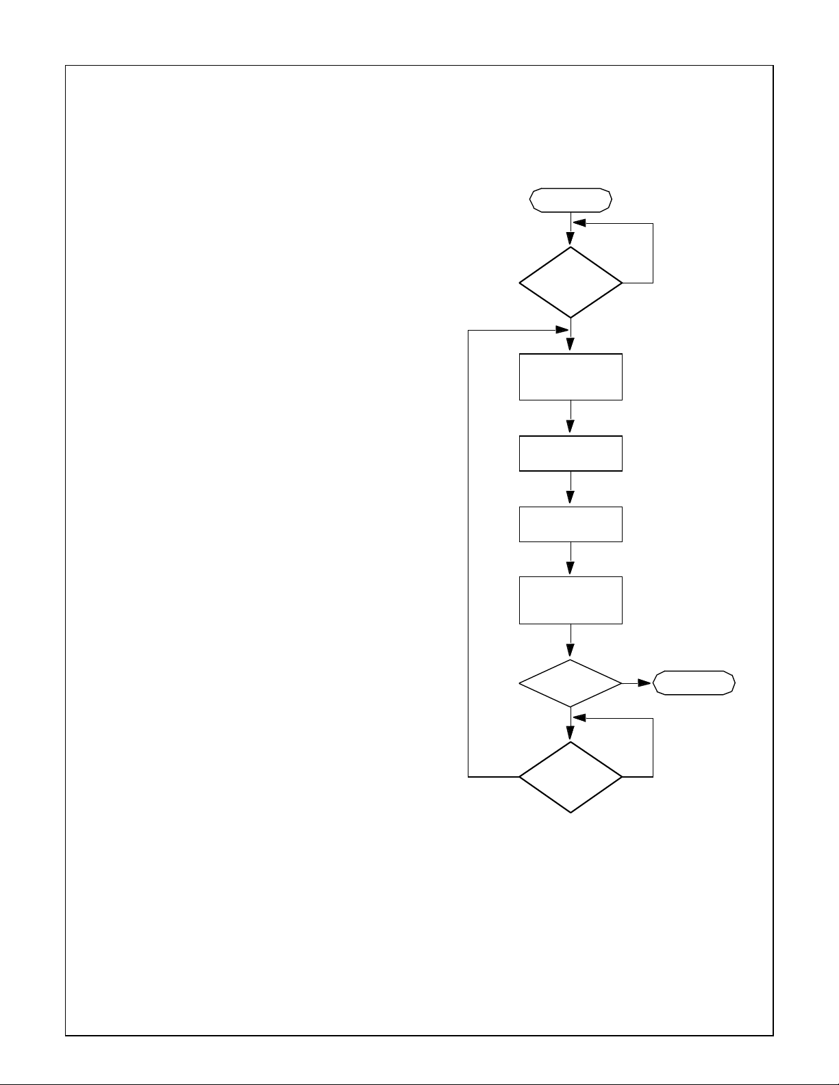
self as no instruction or data can be fetched from it while it is
being programmed. All program and erase operations must
be preceded immediately by writing the proper key to the program memory key register PGMKEY.
The flash EEPROM program memory is divided into 256
pages, each page containing 64 words (each 16 bits wide).
Each page is further divided into two adjacent rows. A page
erase will erase one page. Programming is done by writing to
all the words within a row, one word following another sequentially within one single high voltage pulse. This is supported through a double-buffered write-data buffer scheme.
Byte programming is not supported. Programming should be
done on erased rows.
A mass erase requires the following code sequence (assuming that this sequence will not be interrupted to do another
flash erase or programming):
1. Check for MSTAT.PGMBUSY not set.
2. Set up flash timing reload registers for mass erase operation.
3. Set FLCSR.MERASE = 1.
4. If interrupt was enabled, disable interrupt.
5. Write proper key value to PGMKEY.
6. Write to any valid location within the flash EEPROM program memory.
7. If interrupt was disabled in step 4, re-enable interrupt.
8. Wait for MSTAT.PGMBUSY to clear.
9. Set FLCSR.MERASE = 0.
10. Restore flash timing reload registers for normal operation.
A page erase requires the following code sequence (assuming that this sequence will not be interrupted to do another
flash erase or programming):
1. Check for MSTAT.PGMBUSY not set.
2. Set FLCSR.ERASE = 1.
3. If interrupt was enabled, disable interrupt.
4. Write proper key value to PGMKEY.
5. Write to any valid location within the page to be erased.
6. If interrupt was disabled in step 3, re-enable interrupt.
7. Set FLCSR.ERASE = 0.
When programming, the data to be written into the flash EEPROM program memory is first written into a double-buffered
write-data buffer. When a piece of data is written to the page
while the flash EEPROM program memory is idle, the write
cycle will start. Due to the double-buffered nature of the writedata buffer, a second word can be written to the flash EEPROM program memory. This will then set FLCSR.PMLFULL flag indicating the buffer is now full. When the first write
is done, the memory address would be incremented, and the
second word would be written to that address while keeping
the high voltage pulse active; the FLCSR.PMLFULL flag is
cleared. Another word can then be written to the buffer, and
this programming will repeat until there are no more words to
be programmed. This allows pipelined writes to different
words on the same row within the same high voltage pulse.
If the programming sequence exceeds a row, the flash programming interface will automatically initiate a programming
pulse for the next row. The FLCSR.PMLFULL bit is also
cleared when programming of the last word of the current
row is completed, e.g. programming of the entire row is completed and MSTAT.PGMBUSY is cleared. This means, the
separation of the program memory into rows is transparent to
the user, as the transition is handled by the flash program
memory interface. Figure 3 shows a flowchart for a programming sequence.
start
Yes
No
Yes
done
MSTAT.PGMBUSY
disable interrupt
if necessary
write PGMKEY
write memory
re-enable interrupt
if necessary
Yes
FLCSR.PMLFULL
=1?
No
last word?
No
=0?
Figure 2.Programming Sequence for
the Program Memory
9.1.5 Erase and Programming Timing
The internal hardware of the device handles the timing of
erase and programming operations. To drive the timing control circuits, the device divides the system clock by a programmable prescaler factor. You should select a prescaler
value to produce a program/erase clock of 200 kHz (or as
close as possible to 200 kHz without exceeding 200 kHz).
For the timing control circuit to operate correctly, you must
23 www.national.com

program the prescaler value in advance and leave it unchanged while a program or erase operation is in progress.
A similar (but separate) prescaler factor is applied to the EEPROM data memory. See Section9.1.7 and Section9.3.4 for
details.
9.1.6 Flash EEPROM Program Memory Control and
Status Register (FLCSR)
The Flash EEPROM Program Memory Control and Status
(FLCSR) register is a byte-wide, read/write register that contains several status and control bits related to the program
memory. All reserved bits must be written with 0 for the memory to operate properly when writing to this register. Upon reset, this register is cleared to zero when the flash memory on
the chip is in the idle state.
The register format is shown below.
7 6 4 3 2 1 0
MERASE Reserved PMLFULL PMBUSY PMER Reserved
PMER Flash EEPROM Program Memory page erase.
When set (1) with MERASE bit cleared, a valid
write to the flash EEPROM program memory
erases the entire flash EEPROM program
memory page pointed to by the write address
rather than performing a write to the addressed
memory location.
PMBUSY Program Memory Busy. This bit is automatical-
ly set to 1 when the flash EEPROM program
memory is busy being programmed, and
cleared to 0 at all other times. (The MSTAT.PGMBUSY is also set to 1 whenever the PMBUSY
bit is set to 1.)
PMLFULL Program Memory Write-Latch Buffer Full.
When set (1), the double-buffered data register
for program memory write operations is full.
When cleared (0), the double-buffered data
register is not full.
MERASE Mass Erase Flash EEPROM Program Memory
Array. When set (1) in ISP or test mode, a valid
write to the flash EEPROM program memory
performs an erase to the whole flash EEPROM
program memory rather than perform a write to
the addressed memory location. However, it is
necessary to enter new values into the
FLERASE and FLEND registers to adjust the
mass erase timing before starting the mass
erase.
9.1.7 Program Memory Timing Prescaler Register
(FLPSLR)
The FLPSLR register is a byte-wide, read/write register that
selects the prescaler divider ratio for the flash EEPROM program memory programming clock. Before you program or
erase the program memory for the first time, you should program the FLPSLR register with the proper prescaler value,
an 8-bit value called FTDIV. The device divides the system
clock by (FTDIV+1) to produce the program memory programming clock.
You should choose a value of FTDIV to produce a clock of the
highest possible frequency that is equal to or just less than
200 kHz. For example, if the system clock frequency is 12.5
MHz, use the value 3E hex (62 decimal) for FTDIV, because
12.5 MHz / (62+1) = 198.4 kHz. Do not modify this register
while a flash EEPROM program or erase operation is in
progress.
Upon reset, this register is programmed by default with the
value 63 hex (99 decimal), which is an appropriate setting for
a 20 MHz system clock.
9.1.8 Program Memory Start Time Reload (FLSTART)
The FLSTART register is a byte-wide read/write register that
controls the program and erase start delay time. This value
is loaded into the lower 8 bits of the flash timing counter, and
at the same time, 002 is loaded into the upper 2 bits. Before
you program or erase the program memory for the first time,
program the FLSTART register with the proper prescaler value, FTSTART. The flash timing counter generates a delay of
(FTSTART+1) prescaler output clocks. The default value
provides a delay time of 10µs when the prescaler output
clock is 200kHz. Do not modify this register while a program
or erase operation is in progress.
Upon reset, this register resets to 0116 when the flash memory on the chip is in an idle state.
9.1.9 Program Memory Transition Time Reload
Register (FLTRAN)
The FLTRAN register is a byte-wide read/write register that
controls some program/erase transition times. This value is
loaded into the lower 8 bits of the flash timing counter, and at
the same time, 002 is loaded into the upper 2 bits. Before you
program or erase the program memory for the first time, you
should program the FLTRAM register with the proper prescaler value, FTTRAN. The flash timing counter generates a
delay of (FTTRAN + 1) prescaler output clocks. The default
value provides a delay time of 5µs when the prescaler output
clock is 200kHz. Do not modify this register while a program
or erase operation is in progress.
Upon reset, this register resets to 0016 when the flash memory on the chip is in an idle state.
9.1.10 Program Memory Programming Time Reload
Register (FLPROG)
The FLPROG register is a byte-wide read/write register that
controls the programming pulse width. This value is loaded
into the lower 8 bits of the flash timing counter, and at the
same time, 002 is loaded into the upper 2 bits. Before you
program or erase the program memory for the first time, program the FLPROG register with the proper prescaler value,
FTPROG. The flash timing counter generates a programming
pulse width of (FTPROG + 1) prescaler output clocks. The
default value provides a delay time of 30µs when the prescaler output clock is 200kHz.
Do not modify this register while program/erase operation is
in progress.
Upon reset, this register resets to 0516 when the flash memory on the chip is in idle state.
www.national.com 24

9.1.11 Program Memory Erase Time Reload Register
(FLERASE)
The FLERASE register is a byte-wide read/write register that
controls the erase pulse width. This value is loaded into the
upper 8 bits of the flash timing counter, and at the same time,
112 is loaded into the lower 2 bits. Before you program or
erase the program memory for the first time, program the
FLERASE register with the proper prescaler value, FTER.
The flash timing counter generates a erase pulse width of
4×(FTER + 1) prescaler output clocks. The default value pro-
vides a delay time of 1ms when the prescaler output clock is
200kHz. Do not modify this register while a program or erase
operation is in progress.
Upon reset, this register resets to 3116 when the flash memory on the chip is in idle state.
For mass erase, this value should be changed to C7
generate a pulse width that is four times as long as the page
erase.
9.1.12 Program Memory End Time Reload Register
(FLEND)
The FLEND register is a byte-wide read/write register that
controls the delay time after a program/erase operation. This
value is loaded into the lower 8 bits of the flash timing
counter, and at the same time, 002 is loaded into the upper 2
bits. Before you program or erase the program memory for
the first time, program the FLEND register with the proper
prescaler value, FTEND. The flash timing counter generates
a delay of (FTEND + 1) prescaler output clocks. The default
value provides a delay time of 5µs when the prescaler output
clock is 200kHz. Do not modify this register while program/
erase operation is in progress.
Upon reset, this register resets to 0016 when the flash memory on the chip is in idle state.
For mass erase, this value should be changed to 1316 to provide for a delay time twenty times that of the standard delay.
9.1.13 Program Memory Prescaler Count Register
(FLPCNT)
The FLPCNT register is a byte-wide read-only register that
returns the value of the program memory prescaler counter.
FPCNT contains the flash timing prescaler present count value.
9.1.14 Program Memory Timer Count Register 1
(FLCNT1)
The FLCNT1 register is a byte-wide read-only register that
returns the lower 8 bits of the program memory timing
counter value. FLCNTL is the lower 8 bits of the flash timer
present count value.
9.1.15 Program Memory Timer Count Register 2
(FLCNT2)
The FLCNT2 register is a byte-wide read-only register that
returns the upper 2 bits of the program memory timing
counter value and also the state of the key flash memory interface timing signals. The interface timing signals are only
used in special test modes. Their function is beyond the
scope of this document.
16
to
9.1.16 Program Memory Write Key Register (PGMKEY)
The PGMKEY register is a byte-wide, write-only register that
must be written with a key value (A316) immediately prior to
each write to the flash EEPROM program memory. Otherwise, the write operation to the program memory will fail. This
feature is intended to prevent unintentional programming of
the program memory.
Reading this register always returns FF hex.
Upon reset, the write enable status that is generated as a re-
sult of writing to this key register is cleared.
9.2 RAM MEMORY
The static RAM memory is used for temporary storage of
data and for the program and interrupt stacks. The 3K bytes
of this memory reside in the address range of C000-CBFF
hex. Each memory access requires one clock cycle, for a
byte or word access. No wait cycles or hold cycles are required. For non-aligned word access, each memory access
requires multiple clock cycles.
9.3 FLASH EEPROM DATA MEMORY
The flash EEPROM data memory is used for non-volatile
storage of data. The 2K bytes of low endurance memory reside in the address range of E800-EFFF hex and the 128
bytes of high endurance memory reside in the address range
of F000-F07F hex. The CPU reads or writes this memory by
using ordinary byte-wide or word-wide memory access commands. This memory shares the same array as the ISP flash
program memory.
This memory also support flash memory test mode and there
is no read protection or permanent write protection for this
memory.
9.3.1 Reading
The flash EEPROM data memory read accesses can operate without wait cycles with a CPU clock rate of up to 20MHz
in the normal mode. At higher clock rates, read accesses can
operate with one wait state.
The programmed number of wait cycles used (either zero or
one) is controlled by a bit in the Data Memory Control Status
register (DMCSR.ZEROWS). This register is described in
Section9.3.3.
9.3.2 Programming
Before you begin programming the flash EEPROM data
memory, you should set the value in the EEPROM Data
Memory Prescaler register. This register sets the prescaler
used to generate the data memory programming clock from
the system clock, as described in Section9.3.4.
A code fetch from ISP flash EEPROM program memory is
not possible while flash EEPROM data memory is being programmed because they share the same memory array.
After the CPU performs a write to the flash EEPROM data
memory, the on-chip hardware completes the EEPROM programming in the background. When programming begins,
the on-chip hardware sets the DMCSR.DMBUSY bit to 1,
and also sets the MSTAT.PGMBUSY bit to 1. When programming is completed, it resets these status bits back to 0. Once
the software writes to the flash EEPROM data memory, it
should not attempt to access the EEPROM data memory
25 www.national.com

again until programming is completed and the status bit is reset to 0.
The device hardware internally generates the voltages and
timing signals necessary for programming. No additional
power supply is required, nor any software required except to
check the status bit for completion of programming. The minimum time required to erase and reprogram a byte or word is
1.1 ms. The programmed values can be verified by using nor-
mal memory read operations. The prescaler output drives a
10-bit counter to generate timing pulses and there are five reload registers to produce various pulse widths.
If a reset occurs during a programming or erase operation,
the operation is terminated. The reset is extended until the
flash memory returns to the idle state. Therefore, the timing
logic and program or erase state machine is not cleared on
reset; they are cleared on power-up with the clear signal active until the bus signals are in a known state.
The flash EEPROM data memory does not have permanent
read-protection or write-protection features like those available for the EEPROM program memory. However, the Data
Memory Write Key Register provides a way to “lock” the data
written to the data memory.
9.3.3 Data Memory Control and Status Register
(DMCSR)
The DMCSR register is a byte-wide, read/write register used
with the flash EEPROM data memory or ISP flash EEPROM
program memory. When writing to this register, all reserved
bits must be written with 0 for the memory to operate properly. There are two status/control bits, as shown in the register
format below.
7 6 5 4 3 2 1 0
Reserved ERASE DMBUSY ZEROWS Reserved
ZEROWS Zero Wait-State Access. When cleared (0), the
flash EEPROM data memory will be read in two
cycles. When set (1), the flash EEPROM data
memory will be read in one cycle.
DMBUSY Data Memory Busy. This bit is automatically set
to 1 when the flash EEPROM data memory or
the ISP flash EEPROM program memory is
busy being programmed, and cleared to 0 at all
other times. (The MSTAT.PGMBUSY is also set
to 1 whenever the DMBUSY bit is set to 1.)
ERASE Erase ISP Flash Program Memory Page.
When set (1) a valid write to the ISP flash EEPROM program memory will erase the entire
ISP flash EEPROM program memory page
pointed to by the write address rather than performing a write to the addressed memory location. This bit should be cleared to 0 and remain
cleared after the write operation.
Upon reset, the DMCSR register is cleared to zero when the
flash memory on the chip is in the idle state.
9.3.4 Data Memory Prescaler Register (DMPSLR)
The DMPSLR register is a byte-wide, read/write register that
selects the prescaler divider ratio for the EEPROM data
memory programming clock. Before you write to the data
memory for the first time, you should program the DMPSLR
register with the proper prescaler value, an 8-bit value called
FTDIV. The device divides the system clock by (FTDIV+1) to
produce the data memory programming clock.
You should choose a value of FTDIV to produce a clock of the
highest possible frequency that is equal to or just less than
200 kHz. Upon reset, this register is programmed by default
with the value 63 hex (99 decimal), which is an appropriate
setting for a 20 MHz system clock.
9.3.5 Data Memory Start Time Reload Register
(DMSTART)
The DMSTART register is a byte-wide read/write register that
controls the program/erase start delay time. This value is
loaded into the lower 8 bits of the flash timing counter, and at
the same time, 002 is loaded into the upper 2 bits. Before you
write to the data memory for the first time, you should program the DMSTART register with the proper prescaler value,
an 8-bit value called FTSTART. The flash timing counter generates a delay of (FTSTART + 1) prescaler output clocks. The
default value provides a delay time of 10µs when the prescaler output clock is 200kHz. Do not modify this register while
program/erase operation is in progress.
Upon reset, this register resets to 0116 when the flash memory on the chip is in idle state.
9.3.6 Data Memory Transition Time Reload Register
(DMTRAN)
The DMTRAN register is a byte-wide read/write register that
controls some program/erase transition times. This value is
loaded into the lower 8 bits of the flash timing counter, and at
the same time, 002 is loaded into the upper 2 bits. Before you
write to the data memory for the first time, you should program the DMTRAN register with the proper prescaler value,
an 8-bit value called FTTRAN. The flash timing counter generates a delay of (FTTRAN + 1) prescaler output clocks. The
default value provides a delay time of 5µs when the prescaler
output clock is 200kHz. Do not modify this register while program/erase operation is in progress.
Upon reset, this register resets to 0016 when the flash memory on the chip is in idle state.
9.3.7 Data Memory Programming Time Reload
Register (DMPROG)
The DMPROG register is a byte-wide read/write register that
controls the programming pulse width. This value is loaded
into the lower 8 bits of the flash timing counter, and at the
same time, 002 is loaded into the upper 2 bits. Before you
write to the data memory for the first time, you should program the DMPROG register with the proper prescaler value,
an 8-bit value called FTPROG. The flash timing counter generates a programming pulse width of (FTPROG + 1) prescaler output clocks. The default value provides a delay time of
30µs when the prescaler output clock is 200kHz. Do not modify this register while program/erase operation is in progress.
Upon reset, this register resets to 0516 when the flash memory on the chip is in idle state.
www.national.com 26

9.3.8 Data Memory Erase Time Reload Register
(DMERASE)
The DMERASE register is a byte-wide read/write register
that controls the erase pulse width. This value is loaded into
the upper 8 bits of the flash timing counter, and at the same
time, 112 is loaded into the lower 2 bits. Before you write to
the data memory for the first time, you should program the
DMERASE register with the proper prescaler value, an 8-bit
value called FTER. The flash timing counter generates a
erase pulse width of 4×(FTER + 1) prescaler output clocks.
The default value provides a delay time of 1ms when the
prescaler output clock is 200kHz. Do not modify this register
while program/erase operation is in progress.
Upon reset, this register resets to 3116 when the flash memory on the chip is in idle state.
For mass erase, this value should be changed to C716 when
the flash EEPROM data memory goes to idle mode.
9.3.9 Data Memory End Time Reload Register
(DMEND)
The DMEND register is a byte-wide read/write register that
controls the delay time after a program/erase operation. This
value is loaded into the lower 8 bits of the flash timing
counter, and at the same time, 002 is loaded into the upper 2
bits. Before you write to the data memory for the first time,
you should program the DMEND register with the proper
prescaler value, an 8-bit value called FTEND. The flash timing counter generates a delay of (FTEND + 1) prescaler output clocks. The default value provides a delay time of 5µs
when the prescaler output clock is 200kHz. Do not modify
this register while program/erase operation is in progress.
Upon reset, this register resets to 0016 when the flash memory on the chip is in idle state.
For mass erase, this value should be changed to 1316.
9.3.10 Data Memory Prescaler Count Register
(DMPCNT)
The DMPCNT register is a byte-wide read-only register that
returns the value of the data memory prescaler counter.
FPCNT is the flash timing prescaler present count value.
9.3.11 Data Memory Timer Count Register (DMCNT)
The DMCNT register is a word-wide read-only register that
returns the data memory timing counter value. The reserved
bits return 0000002.
FTCNT[0:9] is the flash timer present count value.
9.3.12 Data Memory Write Key Register (DMKEY)
The DMKEY register is a byte-wide, read/write register that
provides a way to “lock” the data contained in the EEPROM
data memory. Upon reset, the register is automatically set to
C9 hex, which is the key value. Writing to the EEPROM data
memory is allowed as long as the DMKEY register contains
this value. When the register contains any value other than
C9 hex, writing the EEPROM data memory is disallowed.
To “lock” the current data stored in the data memory, write another value (such as 00 hex) to the DMKEY register. To “unlock” the data memory, write the value C9 hex to the DMKEY
register.
Note: Operation of this register is different in from the
PGMKEY register used with the program memory. It is not
necessary to write the key value to DMKEY every time you
write to the data memory.
9.4 ISP MEMORY
The In-System Program memory is part of the flash memory
array that contains the flash EEPROM data memory. It is not
possible to access the ISP memory while programming the
flash EEPROM data memory or access the flash EEPROM
data memory while programming the ISP memory. The 1.5K
bytes of ISP memory resides in the address range of E000E5FF and is used for storing the boot ROM. The ROM contains the code that performs in-system programming, and is
programmed at the factory. In ISP mode, code execution
starts at address E000.
The ISP program memory and flash EEPROM data memory
share the same memory array, which makes it impossible to
access one type of memory while the other is being programmed.
The ISP memory has the following features:
— 1.5K bytes flash EEPROM program memory
— Page size of 4 words, divided into two rows of 2 words
each
— Odd and even bytes within a page can be erased sep-
arately
— 30µs programming pulse width per word
— Page mode erase with 1ms pulse, mass erase with
4ms pulse
— All erased memory bits read 1
— Fast read access time
— Requires valid key for program and erase to proceed
— Provide memory protection and security features for
flash EEPROM program memory
— Security features may limit accesses to ISP memory
— Disable memory when address is out of range to pre-
vent accessing data memory
— Mass erase only allowed in test modes
— Provide busy status during programming and erase
— Read/write accesses disabled during programming/
erase
— Programming high voltage and timing generated on-
chip
9.4.1 Reading
The ISP flash EEPROM program memory read accesses
can operate without wait cycles with a CPU clock rate of up
to 20MHz in the normal mode. At higher clock rates, read accesses can operate with one wait state.
The programmed number of wait cycles used (either zero or
one) is controlled by BIU Configuration (BCFG) register and
the Static Zone 1 Configuration (SZCFG1) register. These
registers are described in Section8.0.
9.4.2 User-Coded Programming Routines
All program and erase operations must be preceded by writing the proper key to the program memory key register ISPKEY. The programming code can be in-system RAM, but
cannot be from ISP flash EEPROM program memory or flash
EEPROM data memory as accesses within these ranges are
27 www.national.com

not permitted while ISP flash EEPROM program memory is
being programmed.
The ISP flash memory is divided into 192 pages, each page
containing 4 words (each 16 bits wide). Each page is further
divided into two rows. Erase is carried out one page at a time,
whereas programming is carried out one row (or one partial
row) at a time.
Once an erase or programming operation is started, the PGMBUSY bit in the MSTAT register is automatically set, and
then cleared when the operation is complete. All high-voltage
pulses and timing needed for programming and erasing are
provided internally. The program memory cannot be accessed while the PGMBUSY bit is set.
Erase Procedure
Erasing a page requires the following code sequence:
1. Verify that the MSTAT.PGMBUSY bit is cleared.
2. Set the DMCSR.ERASE bit to 1.
3. Locally disable interrupts.
4. Write proper key value to the ISPKEY register.
5. Write to any valid page to be erased.
6. Re-enable interrupts disabled in Step 3.
7. Set the DMCSR.ERASE bit to 0.
9.4.3 Programming Procedure
Programming is done by writing one byte or word at a time
and should be done on already erased memory.
Programming the ISP flash EEPROM program memory requires the following code sequence:
1. Verify that the MSTAT.PGMBUSY bit is cleared.
2. Locally disable interrupts.
3. Write proper key value to the ISPKEY register.
4. Write a byte or word to the addressed location.
5. Re-enable interrupts disabled in Step 2.
Programmed values can be verified through normal read operations.
If a reset occurs in the middle of an erase or programming
operation, the operation is terminated. The reset is extended
until the flash EEPROM memory returns to the idle state.
9.4.4 Erase and Programming Timing
The program and erase timing are controlled by the flash EEPROM data memory logic.
9.4.5 Memory Control and Protection Features
The last 8 bytes of the ISP memory are reserved for special
functions and some of these bytes provide memory protection and security for the flash EEPROM program memory.
Read and various types of write protection are provided.
During the reset stretch period, bytes located at E5FE and
E5FF are read out to the FLCTRL2 and FLSEC registers respectively. Upon reset and before an instruction fetch, bytes
located at E5FC and E5FD are read out to the FLCTRL2 and
FLCTRL1 registers respectively. Parts of FLCTRL2 register
are loaded at different times.
E5FE Byte
Upon reset of the chip, the byte located at E5FE is read into
the FLCTRL2 register. It can be written in the ISP or test environments. It can also be written in the IRE environment
through a byte write instruction when the write instruction is
anywhere within the user boot ROM area (defined above) except for the last two words. When the user boot ROM area
has been disabled, this word cannot be programmed in the
IRE environment. Note that when this word is erased for reprogramming, the other words in the same page must first be
saved, and then re-programmed.
7 5 4 2 1 0
EMPTY Reserved CODEAREA[9:8]
CODEAREA[9:8]
The 2 least significant bits in address E5FE
contains the two most significant bits of the 10bit CODEAREA field. The description of
CODEAREA is shown in the E5FC section.
EMPTY The EMPTY status indicates if the flash EE-
PROM program memory array is empty or not.
It is located in the 3 most significant bits in address E5FE. When two or more bits in the
EMPTY field are set, the flash EEPROM program memory is empty. Upon reset of the device and the environment select pins are all
high, the device operates in ISP environment
rather than IRE environment. After the program
memory has been filled with user code, this
field should be cleared to 0002.
000, 001, 010, 100: Program memory contains user code
011, 101, 11x: Program memory is empty, do not start up in IRE
E5FF Byte
Upon reset, the byte located in the E5FF address is read into
the FLSEC register. This byte cannot be written to in the IRE
environment. The format of the E5FF byte is shown below:
7 4 3 0
FROMWR FROMRD
The FROMRD and FROMWR fields in address location
E5FF respectively provide read and write security to the flash
EEPROM program memory array while executing instructions in all environments except IRE. The user should always
write 00002 to enable security feature.
0000, 0001, 0010, 0100, 1000: Security feature enabled
0011, 0101, 011x, 1001, 101x, 11xx: Security feature disabled
FROMRD Upon reset of the chip, read security is enabled
and 0000 is returned in all environments except
IRE. The internal program code can only be executed in the IRE environment when read security is activated.
FROMWR Upon reset of the chip, write security is enabled
and program and erase operations to the flash
EEPROM program memory in either programming modes are prevented.
Once read/write security is enabled, the odd numbered bytes
from address E5F9 to E5FF cannot be erased. Once a security feature has been enabled, it cannot be undone. To prevent the security status from being erased, the ISP and data
memory array cannot be mass erased.
Note: In flash memory test mode, this condition also prevents the odd numbered bytes of the high endurance flash
EEPROM data memory (F001 to F07F) from being erased;
www.national.com 28
however, the even numbered bytes of the high endurance
6 0
128)+127
flash EEPROM data memory (F000 to F07E) and the ISP
flash EEPROM program memory (E000 to E5FE) can be
erased.
Read/write is overridden through PADX.
E5FC Byte
Upon reset of the chip, E5FC is read into the FLCTRL2 register. The byte at E5FC is written in the ISP or test environments, or in the IRE environment through a byte-write
instruction when the write instruction is anywhere within the
user boot ROM area except for the last two words. When the
user boot ROM area has been disabled by having a value of
7F16 in BOOTAREA, this word cannot be programmed in the
IRE environment. Note that when this word is erased for reprogramming, the other words in the same page must first be
saved, and then re-programmed also. The E5FC register format is shown below:
7 0
CODEAREA[7:0]
This byte contains the lowest 8 bits of the CODEAREA field.
When appended to the left with the lowest 2 bits in the address E5FE, it forms the complete CODEAREA field, which
provides write protection to all or part of the program memory, see Figure3. When write security is not enabled and
CODEAREA does not contain the value 3FF16, the program
memory range from (CODEAREA×128) to 1FFFF is consid-
ered as protected user code area and cannot be written. The
minimum protected memory range is therefore 256 bytes
when CODEAREA contains the value 3FE. Note that the
C000-FFFF memory range is not considered as program
memory and is not protected by CODEAREA.
E5FD Byte
Upon the reset of the chip, the byte located at the E5FD address is read into the FLCTRL1 register. This byte can only
be written in the ISP or test environments but not in the IRE
environment. If this byte is erased for re-programming, the
user must first save the other bytes in the same page, and
then re-program those bytes. The format of the E5FD byte is
shown below:
7
Reserved BOOTAREA
BOOTAREA provides write protection to part of the program
memory, see Figure4. When the write security feature is not
enabled and BOOTAREA does not contain the value 7F16,
then the program memory range from 0 to (BOOTAREA*128)+127 is considered as user boot ROM area and cannot be written to. The maximum protected memory range is
therefore 16K-127 bytes when BOOTAREA contains the value 7E16.
1FFFFh
boot area maximum limit
3F80h
(BOOTAREA×
protected user boot
area
0000h
CR16MHR6
Address Map
1FFFFh
10000h
C000h
0000h
protected user
code area
non-code area, not
protected
protected user
code area
CR16MHR6
Address Map
CODEAREA×128
Figure 3.Memory Protection through CODEAREA
When CODEAREA contains the value 3FF16, write protection is disabled. When the user code area overlaps into the
user boot ROM area, the overlap area is governed by a more
restrictive write protection feature, which is the user boot
ROM area. When write security has been enabled, the entire
program memory area is already write protected in all environments.
Note that when a new value is written into CODEAREA, write
protection controlled by CODEAREA is updated after the
next device reset.
Figure 4.Memory Protection through BOOTAREA
When BOOTAREA contains the value 7F16, write protection
is disabled. When write security has been enabled, the entire
program memory area is already write protected in all environments.
Note that when a new value is written into BOOTAREA, write
protection controlled by BOOTAREA is updated after the
next device reset.
9.4.6 Test Mode
The ISP flash EEPROM program memory test mode allows
direct access to the flash memory from the device pins, and
bypasses the CR16B core. This test mode also accesses the
flash memory cells that are not used in data memory (three
out of four bytes in each page).
9.4.7 Flash Program Memory Control Register 1
(FLCTRL1)
The FLCTRL1 register is a read-only byte-wide register. The
value of this register is loaded from memory address E5FD
16
when the chip comes out of reset. The BOOTAREA field defines a user boot ROM area to be write protected. The Flash
EEPROM Program Memory Control Register 1 format is
shown below:
7 6 0
Reserved BOOTAREA
29 www.national.com
When BOOTAREA has any value other than 7F16, then the
7 0
memory at 0 to (BOOTAREA×128)+15 is considered as user
boot ROM area and is write protected. When it has a value of
7F16, then there is no user boot ROM area to be write protected
9.4.8 Flash Program Memory Control Register 2
(FLCTRL2)
The FLCTRL2 register is a read-only word-wide register. The
value of this register is loaded from memory addresses
E5FC16 and E5FE16 when the chip comes out of reset. When
the device starts execution, the EMPTY bit indicates whether
the flash EEPROM program memory is empty of not, and selects the chip to be in IRE or ISP environment if the external
environment pins are all high. The CODEAREA field defines
a user code area to be write protected. The Flash EEPROM
Program Memory Control Register 2 format is shown below:
15 13 12 10 9 0
EMPTY Reserved CODEAREA
9.4.10 ISP Memory Write Key Register (ISPKEY)
The In-System-Programming Memory Write Key (ISPKEY)
register is a byte-wide, write-only register. It contains the enable key to enable writes to ISP flash EEPROM program
memory. A value of 6A16 must be written to this register immediately preceding every write to the ISP flash EEPROM
program memory for the flash write operation to proceed,
otherwise any other write operation will clear the key (the
only exception is that the subsequent write is another write to
this key register with the proper key, in which case the key is
still set). A read always returns FF16. Engineering note: on
reset, the write enable status that is generated as a result of
a write to this key register is cleared. The ISP Memory Write
Key register format is shown below:
ISPKYVAL
EMPTY When the bits are either 0112, 1012, 1102, or
1112, and if the device’s environment select
pins are all high, the device will come out of reset in ISP environment instead of IRE environment.
CODEAREA When it has any value other than 3FF16, then
the memory (CODEAREA×128) to 1FFFF16 is
considered as user code area and is write protected. When it has a value of 3FF16, then there
is no code protection area to be write protected.
9.4.9 Flash Program Memory Security Register
(FLSEC)
The FLSEC register is a read-only byte-wide register. When
the chip comes out of reset, the value of this register is loaded from memory address E5FF16. The FROMRD and
FROMWR field control the read and write security of the flash
EEPROM program memory respectively. The Flash EEPROM Program Memory Security register format is shown
below:
7 4 3 0
FROMWR FROMRD
0000, 0001, 0010, 0100, 1000: Security feature enabled
0011, 0101, 011x, 1001, 101x, 11xx: Security feature disabled
FROMRD When read security feature is enabled, the
flash EEPROM program memory can only be
read in IRE environment, but will return 0000
16
in other environments; also, erase to odd numbered bytes from address E5F916 to E5FF
16
and mass erase to ISP and flash EEPROM
data memory array are ignored unless PADX is
activated (see security override below).
FROMWR Unless PADX is activated (see override below),
when write security feature is enabled, all further writes and erases to flash EEPROM program memory, erase to odd numbered bytes
from address E5F916 to E5FF16, and mass
erase to ISP and flash EEPROM data memory
array are ignored.
ISPKYVAL is the ISP Flash Program Memory Write Enable
Key Value.
www.national.com 30

10.0 Interrupts
The Interrupt Control Unit (ICU31L) receives interrupt requests from internal and external sources and generates interrupts to the CPU. Interrupts from the timers, USARTs,
MICROWIRE/SPI interface, Multi-Input Wake-Up, and A/D
converter are all maskable interrupts. The highest-priority interrupt is the Non-Maskable Interrupt (NMI), which is triggered by a falling edge received on the NMI input pin. The
NMI pin is not available on the 44-pin packages.
10.1 INTERRUPT OPERATION
An exception is an event that temporarily stops the normal
flow of program execution and causes execution of a separate service routine. Upon completion of the service routine,
execution of the interrupted program continues from the point
at which it was stopped.
There are two kinds of exceptions, called traps and inter-
rupts. A trap is the result of some action or condition in the
program itself, such as execution of an Exception (EXCP) instruction. An interrupt is a CPU-external event, such as a signal received on a Multi-Input Wake-Up input or a request
from an on-chip peripheral module for service.
The operation of traps is beyond the scope of this data sheet.
For information on traps, and for additional detailed information on interrupts not provided in this data sheet, please refer
to the CompactRISC CR16B Programmer's Reference Manual.
10.1.1 Interrupt Operation Summary
When an interrupt occurs, the on-chip hardware performs the
following steps:
1. Decrements the Interrupt Stack Point (ISP) by four.
2. Saves the contents of the Program Counter (PC) and
Processor Status Register (PSR) on the interrupt stack.
3. Clears the I, P, and T bits in the Processor Status Register (PSR). These are the Global Maskable Interrupt
Enable bit, Trace Trap Pending bit, and Trace bit, respectively.
4. Reads the interrupt vector from the Interrupt Vector Register (IVCT).
5. Combines the interrupt vector with the value in the Interrupt Base (INTBASE) register to obtain an address in
the Interrupt Dispatch Table, and loads the dispatch table entry into the Program Counter (PC).
From this point onward, the CPU executes the interrupt service routine. The service routine ends with a Return from Exception (RETX) instruction. This returns the CPU to the
interrupted program. The CPU restores the contents of the
PC and PSR registers from the stack and increments the Interrupt Stack Pointer by four.
10.1.2 Service Routine Addresses
When an interrupt or trap occurs, the CPU executes a service routine. There are different service routines for different
interrupts and traps. Each service routine may reside anywhere in program memory. The starting addresses of the service routines are contained in a table called the Dispatch
Table. Entries in the table are organized in the order shown
in Table10.
Table 10Dispatch Table Entries
0: Reserved
1: NMI
2: Reserved
3: Reserved
4: Reserved
5: SVC (Supervisor Call Trap)
6: DVC (Divided by Zero Trap)
7: FLG (Flag Trap)
8: BPT (Breakpoint Trap)
9: TRC (Trace Trap)
10: UND (Undefined Instruction Trap)
11: Reserved
12: Reserved
13: Reserved
14: Reserved
15: Reserved
16: INT0 (Reserved)
17: INT1 (Flash EEPROM Program Memory)
18: INT2 (Reserved)
19: INT3 (Reserved)
20: INT4 (Reserved)
21: INT5 (ADC)
22: INT6 (MIWU Interrupt 3)
23: INT7 (MIWU Interrupt 2)
24: INT8 (MIWU Interrupt 1)
25: INT9 (MIWU Interrupt 0)
26: INT10 (USART 2 Tx)
27: INT11 (USART 1Tx)
28: INT12 (Reserved)
29: INT13 (MICROWIRE/SPI Rx/TX)
30: INT14 (ACCESS.bus)
31: INT15 (USART 2 Rx)
32: INT16 (USART 1 Rx)
33: INT17 (Reserved)
34: INT18 (CAN)
35: INT19 (Reserved)
36: INT20 (Reserved)
37: INT21 (Reserved)
31 www.national.com

Table 10Dispatch Table Entries
38: INT22 (Reserved)
39: INT23 (VTUD Interrupt Request 4)
40: INT24 (VTUD Interrupt Request 3)
41: INT25 (VTUD Interrupt Request 3)
42: INT26 (VTUD Interrupt Request 1)
43: INT27 (T2B Timer 2 Interrupt B)
44: INT28 (T2A Timer 2 Interrupt A)
45: INT29 (T1B Timer 1Interrupt B)
46: INT30 (T1A Timer 1Interrupt A)
47: INT31 (RTI Timer 0)
Each entry in the Dispatch Table consists of two bytes that
provide bits 1 through 16 of the starting address of the corresponding service routine. The full 21-bit address of a service
routine is reconstructed by adding a leading 0 and a trailing
0 to the 16-bit table entry.
The INTBASE register is a pointer to the Dispatch Table.
Upon reset, the initialization software must write the starting
address of the Dispatch Table to the INTBASE register, a 21bit register with the five most significant bits and the least significant bit always equal to 0. It is typically kept in the flash
EEPROM program memory. The Dispatch Table is 48 words
long.
Each interrupt or trap source has an associated vector number ranging from 0 to 31, as indicated in Table10. When an
interrupt occurs, the hardware multiplies the vector by 2,
adds the result to the contents of the INTBASE register, and
uses the resulting address to obtain the service routine starting address from the corresponding entry in the Dispatch Table. This address is placed in the Program Counter so that
the CPU begins executing the interrupt service routine.
Figure5 summarizes the method used by the device to generate the starting address of a service routine.
10.1.3 Stack Usage
When an interrupt occurs, the CPU automatically preserves
the contents of the Program Counter (PC) and Processor
Status Register (PSR) by pushing them on the interrupt stack
and decrementing the Interrupt Stack Pointer by four. The
service routine ends with a Return from Exception (RETX) instruction, which returns control to the interrupted program by
restoring the PC and PSR values and incrementing the Interrupt Stack Pointer (ISP) by four.
Prior to using any interrupts, the Interrupt Stack Pointer (ISP)
must be initialized so that it points to a space in RAM where
the interrupt stack will be kept. The stack grows downward in
memory (toward address zero) when an interrupt occurs and
items are pushed onto the stack. The stack shrinks upward
in memory when an interrupt service routine ends and items
are popped from the stack.
Many routines need to use the general-purpose registers R0
through R13. To preserve the existing register contents, a
routine can save register contents on the program stack upon
start of the routine and restore the register contents prior to
completion of the routine. The software can also use the program stack to transfer data parameters from one routine to
another when the parameters are too large to easily fit into
the registers. A high-level language typically allocates the local (non-static) variables on the stack.
The pointer to the program stack is the SP register, which
must be initialized prior to any register save/restore operations or data transfer operations. Using the program stack, an
interrupt routine needs to initially save the contests of all registers that it uses, and restore those register contents before
returning to the interrupted program.
10.2 NON-MASKABLE INTERRUPT
A non-maskable interrupt is triggered by a falling edge on the
NMI input pin, which generates a software trap. The NMI pin
is an asynchronous input with Schmitt trigger characteristics
and an internal synchronization circuit. Therefore, no external synchronizing is needed.
Upon reset, the non-maskable interrupt is disabled and
should remain disabled until the software initializes the interrupt table, interrupt base, and interrupt stack pointer. It can
be enabled by setting either of two control bits in the External
NMI Control/Status (EXNMI) register. The two bits are called
the EN (Enable) bit and the ENLCK (Enable and Lock) bit.
The EN bit enables the NMI trap until an NMI trap event or a
reset occurs. An NMI trap automatically resets the EN bit. Using this bit to enable the NMI trap is intended for applications
where the NMI pin is toggled frequently but nested NMI traps
are not needed. The trap service routine should re-enable the
NMI trap by setting the EN bit before returning to the main
program.
The ENLCK bit enables the NMI trap and locks it in the enabled state. In other words, it leaves the NMI trap enabled
even after the trap occurs. It can be cleared only by a reset
operation. After the bit is set, an NMI trap is triggered by each
falling edge on the NMI pin, allowing nested NMI traps.
To use the EN bit, the ENLCK must remain cleared to 0. Otherwise, the EN bit is ignored.
10.3 MASKABLE INTERRUPTS
Maskable interrupts can be enabled or disabled under software control. There are 31 level-triggered maskable interrupt
sources (including some reserved for future expansion), organized into levels of priority. If more than one interrupt event
occurs at any given time, the interrupt source with the highest
priority is serviced first. The others must wait until the highest-priority interrupt is serviced and is no longer pending.
Figure11 lists the maskable interrupt sources of the device
in order of priority, from the highest-priority interrupt (IRQ31)
to the lowest (IRQ0).
To enable a maskable interrupt, the enable bit must be set in
the applicable peripheral module and also in the appropriate
Interrupt and Enable Mask register, IENAM0 or IENAM1. In
addition, both the Global Maskable Interrupt Enable bit (I)
and the Local Maskable Interrupt Enable bit (E) must be set
to 1 in the PSR register. If either one of these bits is 0, then
all maskable interrupts are disabled. The CR16B core supports IRQ0, but ICU31L reserves IRQ0 so that it is not connected to any interrupt source.
www.national.com 32

INTBASE
~~~
~
31 0
Reserved
0
1
2
3
4
5
NMI
Reserved
Reserved
Reserved
SVC
Non-maskable Interrupt
Supervisor Call Trap
6
7
8
9
10
11
12
13
14
15
16 to 127
Table 11Maskable Interrupt Priority List
Interrupt Request Source
IRQ31 RTI (Timer 0), highest priority
IRQ30 T1A (Timer 1 input A)
IRQ29 T1B (Timer 1 input B)
IRQ28 T2A (Timer 2 input A)
IRQ27 T2B (Timer 2 input B)
IRQ26 VTUA (VTU Interrupt Request 1)
IRQ25 VTUB (VTU Interrupt Request 2)
IRQ24 VTUC (VTU Interrupt Request 3)
IRQ23 VTUD (VTU Interrupt Request 4)
IRQ22-IRQ19 Reserved
IRQ18 CAN
IRQ17 Reserved
IRQ16 USART1 Rx
IRQ15 USART2 Rx
IRQ14 ACCESS.bus
IRQ13 MICROWIRE/SPI Rx/Tx
IRQ12 Reserved
IRQ11 USART1 Tx
IRQ10 USART2 Tx
IRQ9 MIWU16 Interrupt 0
DVZ
FLG
BPT
TRC
UND
Reserved
Reserved
Reserved
DBG Debug Trap
ISE
INTn
Figure 5.
IRQ8 MIWU16 Interrupt 1
IRQ7 MIWU16 Interrupt 2
IRQ6 MIWU16 Interrupt 3
IRQ5 ADC
IRQ4-IRQ2 Reserved
IRQ1 Flash Program Memory
IRQ0 Reserved, lowest priority
Both the E bit and I bit can be controlled with the Load Processor Register (LPR) instruction. In addition, the E bit is
easily changed by executing the Enable Interrupts (EI) or
Disable Interrupts (DI) instruction. Using the EI and DI instructions avoids the possibility of an interrupt occurring within a read-modify-write operation on the PSR register.
Divide By Zero Trap
Flag Trap
Breakpoint Trap
Trace Trap
Undefined Instruction Trap
In-System Emulator Interrupt
Maskable Interrupts
Table 11Maskable Interrupt Priority List
Interrupt Request Source
10.4 INTERRUPT REGISTERS
The Interrupt Control Unit uses the following interrupt control
and status registers:
— Non-Maskable Interrupt Status Register (NMISTAT)
— Non-Maskable Interrupt Status Monitor Reg. (NMIMN-
TR)
— External NMI Control/Status Register (EXNMI)
— Interrupt Enable and Mask Register 0 (IENAM0)
— Interrupt Enable and Mask Register 1 (IENAM1)
— Interrupt Vector Register (IVCT)
33 www.national.com

— Interrupt Status Register 0 (ISTAT0)
— Interrupt Status Register 1 (ISTAT1)
— Interrupt Debug Register (IDBG)
The following CPU core registers are also used in processing
interrupts:
— Interrupt Stack Pointer (ISP)
— Interrupt Base Register (INTBASE)
10.4.1 Non-Maskable Interrupt Status Register
(NMISTAT)
The NMISTAT register is a byte-wide, read-only register that
holds the current pending status of the Non-Maskable Interrupt (NMI). This register is cleared upon reset. It is also
cleared each time it is read. The register format is shown below.
7 6 5 4 3 2 1 0
Reserved EXT
EXT External Non-Maskable Interrupt Request.
When set to 1 by the hardware, it indicates an
external Non-Maskable Interrupt request has
occurred. See the description of the EXNMI
register below for more information.
10.4.2 External NMI Control/Status Register (EXNMI)
The EXNMI register is a byte-wide, read/write register that
shows the current state of the NMI pin and also allows the
NMI trap to be enabled by setting either the EN bit or the ENLCK bit. Both of these bits are cleared upon reset. When the
software writes to this register, it must write 0 to all reserved
bit positions for the device to function properly. EN, ENLCK,
and TST are cleared upon reset. The register format is
shown below.
7 6 5 4 3 2 1 0
Reserved ENLCK PIN EN
EN Enable NMI Trap. When set to 1, NMI traps are
enabled and falling edge on the NMI pin generates a NMI trap. Each occurrence of an NMI
trap automatically clears the EN bit. The trap
service routine should set the EN bit to 1 before
returning control to the interrupted program.
When EN is cleared to 0, NMI traps are disabled unless they are enabled with the ENLCK
bit. When the ENLCK bit is set to 1, the EN bit
is ignored.
PIN NMI Pin. This bit shows the current state of the
NMI input pin (without logical inversion). A 1 indicates a high level and a 0 indicates a low level on the pin. This is a read-only bit. In a write
operation, the value written to this bit position is
ignored.
ENLCK Enable and Lock NMI Trap. When set to 1, NMI
traps are enabled and locked in the enabled
state. Each falling edge on the NMI pin generates a NMI trap, even if a previous NMI trap has
occurred and is still being processed. When
ENLCK is cleared to 0, NMI traps are disabled
unless they are enabled with the EN bit.
10.4.3 Interrupt Vector Register (IVCT)
The IVCT register is a byte-wide, read-only register that contains the encoded value of the enabled and pending
maskable interrupt with the highest priority. The on-chip hardware automatically updates this field whenever there is a
change in the highest-priority enabled and pending maskable
interrupt. The CPU reads this register during an interrupt acknowledge core bus cycle to determine where to begin executing the interrupt service routine. The register contents are
guaranteed to be valid at that time. The register is not guaranteed to contain valid data during a hardware update operation. The register format is shown below.
7 6 5 4 3 2 1 0
0 0 INTVECT
INTVECT Interrupt Vector. This 6-bit field contains the en-
coded value of the enabled and pending
maskable interrupt with the highest priority. For
example, if interrupts IRQ1 and IRQ6 are both
enabled and pending, the higher-priority interrupt is IRQ6. As a result the 6 bit interrupt vector is 010110.
10.4.4 Interrupt Enable and Mask Register 0 (IENAM0)
The IENAM0 register is a word-wide, read/write register that
enables or disables the individual interrupts IRQ0 through
IRQ15. The register format is shown below.
15 0
IENA(15:0)
A bit set to 1 enables the corresponding interrupt. A bit
cleared to 0 disables the corresponding interrupt. Upon reset, this register is initialized to FFFF hex.
10.4.5 Interrupt Enable and Mask Register 1 (IENAM1)
The IENAM0 register is a word-wide, read/write register that
enables or disables the individual interrupts IRQ16 through
IRQ31. The register format is shown below.
15 0
IENA(31:16)
A bit set to 1 enables the corresponding interrupt. A bit
cleared to 0 disables the corresponding interrupt. Upon reset, this register is initialized to FFFF hex.
10.4.6 Interrupt Status Register 0 (ISTAT0)
The ISTAT0 register is a word-wide, read-only register that
indicates which maskable interrupt inputs to the ICU31L
(IRQ0 through IRQ15) are currently active. The register format is shown below.
15 0
IST(15:0)
IST(15:0) Interrupt Status bits. Each bit indicates the cur-
rent status of an interrupt input to the ICU31L,
corresponding to interrupts IRQ0 through
IRQ15. A bit set to 1 indicates an active interrupt input, even when the interrupt is masked
out by the IENAM0 register. A bit cleared to 0
indicates an inactive interrupt input.
www.national.com 34

10.4.7 Interrupt Status Register 1 (ISTAT1)
The ISTAT1 register is a word-wide, read-only register that
indicates which maskable interrupt inputs to the ICU31L
(IRQ16 through IRQ31) are currently active. The register format is shown below.
15 0
IST(31:16)
IST(31:16) Interrupt Status bits. Each bit indicates the cur-
rent status of an interrupt input to the ICU31L,
corresponding to interrupts IRQ16 through
IRQ31. A bit set to 1 indicates an active interrupt input, even when the interrupt is masked
out by the IENAM0 register. A bit cleared to 0
indicates an inactive interrupt input.
10.4.8 Interrupt Debug Register
The IDBG register is a word-wide read-only register, which
contains various status information of the ICU31L. The lowest 6 bits contain the INTVECT value during the last read
from address FE00. The next 6 bits contain the INTVECT
value when a maskable interrupt request is sent to the
CR16B core. Upon reset, this register is set to 0000 hex.
10.5 INTERRUPT PROGRAMMING
PROCEDURES
The following subsections provide information on initializing
the device for interrupts, clearing interrupts, and nesting interrupts.
10.5.1 Initialization
Upon reset, all interrupts are disabled. To program the device
for interrupt operation and to enable interrupts, use the following procedure in the application software:
1. Set the Interrupt Stack Pointer (ISP)
2. Load the INTBASE register so that it points to the base
of the Interrupt Dispatch Table.
3. Perform any required preparation steps for the interrupt
service routines.
4. Initialize the peripheral devices that can generate interrupts and set their respective interrupt enable bits.
5. Set the relevant bits in the interrupt mask registers
(IENAM0 and IENAM1)
Note: The MIWU16 interrupts have no local interrupt enable bits, which means you can only disable the
MIWU16 interrupts if you clear the specific bits in the IENAM register.
6. Use the Load Processor Register (LPR) instruction to
set I bit in the PSR register.
7. When the device is ready to execute interrupts, set the
E bit in the PSR register by executing the Enable Interrupts (EI) instruction.
Once maskable interrupts are enabled by setting the E and I
bits, you can disable and re-enable all maskable interrupts
locally by using the Enable Interrupts (EI) and Disable Interrupts (DI) instructions, which set and clear the E bit.
10.5.2 Clearing Interrupts
Clearing an interrupt request before it is serviced may cause
a spurious interrupt because the CPU may detect an interrupt not reflected in the Interrupt Vector (IVCT) register. To
ensure reliable operation, clear interrupt requests only while
interrupts are disabled.
Changing the polarity of an interrupt input (for example, in the
Multi-Input Wake-Up module) can cause a spurious interrupt,
and therefore should be done only while interrupts are disabled.
For the same reason, clearing an enable bit in a peripheral
module should be carried out only while the interrupt is disabled.
10.5.3 Nesting Interrupts
Interrupts may be nested, or in other words, an interrupt service routine can itself be interrupted by a different interrupt
source. There is no hardware limitation on the number of interrupt nesting levels. However, the interrupt stack must not
be allowed to overflow its allocated memory space.
Unless specifically enabled by the software, nested interrupts will not occur. When the CPU acknowledges an interrupt, the I bit in the PSR register is automatically cleared to 0
for the duration of the service routine, disabling any further
maskable interrupts.
To allow nested interrupts, an interrupt service routine should
first set or clear the respective interrupt enable bits to specify
which peripherals will be allowed to interrupt the current service routine. The present interrupt routine should be disabled
(or interrupt pending bit cleared). The service routine should
then set the PSR.I bit to 1, thus enabling maskable interrupts.
This bit can be controlled with the Store Processor Register
(SPR) and Load Processor Register (LPR) instructions.
Note:
Clearing the pending bit of the current interrupt should not be
immediately followed by enabling further interrupts by setting
the I bit in the PSR register. Wait states must be inserted into
the software after clearing the interrupt pending bit and before another interrupt. Placing a NOP instruction will perform
this instruction. This is because the instruction which resets
the pending bit may not yet be finished when the interrupts
are already enabled again by setting the I bit in the PSR register. To avoid this situation the user has to make sure that
prior to enabling the interrupt an additional instruction is inserted. This could look like the example below:
SBITi $0, T1ICRL # clear pending bit
NOP # NOP instruction
MOVW $0x0a00, r0 # enable further interrupts
LPR r0, psr
A CBITi or SBITi instruction may be used to clear the interrupt
pending bit. In such cases, a spurious interrupt may occur.
35 www.national.com

11.0 Power Management
The Power Management Module (PMM) improves the efficiency of the device by changing the operating mode (and
therefore the power consumption) according to the required
level of device activity.
The device can operate in any of four power modes:
— Active
— Power Save
— Idle
— Halt
Table12 summarizes the main properties of the four operating modes: the state of the high-frequency oscillator (on or
off), the type of clock used by most modules, and the clock
used by the Timing and Watchdog Module (TWM).
Table 12Power Mode Operating Summary
Mode
Active On Main Clock Slow Clock
Power Save On or Off Slow Clock Slow Clock
Idle On or Off None Slow Clock
Halt Off None None
The low-frequency oscillator continues to operate in all four
modes and power must be provided continuously to the device power supply pins. In the Halt mode, however, the internal SLCLK does not toggle, and as a result, the TWM timer
and Watchdog Module do not operate. For the Power Save
and Idle modes, the high-frequency oscillator can be turned
on or off under software control, as long as the low-frequency
oscillator is used.
11.1 ACTIVE MODE
In the Active mode, all device modules are fully operational.
This is the operating mode upon reset. Most device modules
use the clock generated by the high-frequency clock oscillator. The clock rate is determined by the external crystal network.
Power consumption in the Active mode can be reduced by
selectively disabling unused modules and/or by executing
the WAIT instruction. When WAIT is executed, the core stops
executing new instructions and waits for an interrupt.
11.2 POWER SAVE MODE
In the Power Save mode, all device modules operate off the
low-frequency clock. If the low-frequency clock is generated
from an external crystal network, the high-frequency clock
oscillator can be turned off to further reduce power consumption.
All on-chip modules continue to operate in the Power Save
mode, with the SLCLK acting as their system clock. If this
mode is entered by using the WAIT command, the CPU is inactive and waits for an interrupt to wake up. Otherwise, CPU
continues to function normally at the lower frequency of the
slow clock.
The low frequency of the clock in Power Save mode limits the
operation of modules such as the USARTs, MICROWIRE interface, A/D Converter, and timers because they are driven
High-Frequency
Oscillator
Clock Used TWM Clock
by the slow clock rather than the normal high-speed clock. In
order to work properly in Power Save mode, modules that
perform real-time operations (such as a USART baud rate
generator) must be reprogrammed to use the slower clock.
To reduce power consumption as much as possible, the program should execute a WAIT instruction during periods of
CPU inactivity.
11.3 IDLE MODE
In the Idle mode, the clock is stopped for most of the device.
Only the Power Management Module and Timing and Watchdog Module continue to operate. Both of these modules use
the slow clock in this mode.
11.4 HALT MODE
In the Halt mode, all device clocks are disabled and the highfrequency oscillator is shut off. In this mode, the device consumes the least possible power while maintaining the device
memory and register contents. The low-frequency oscillator
continues to operate in this mode, but with very low power
consumption due to its power-optimized design.
11.5 CLOCK INPUTS AND RESET
CONFIGURATION
The system uses a high frequency clock Active mode. The
source of this clock in the device is a high frequency crystal
oscillator. The Oscillating High Frequency Clock (OHFC) input indicates to the Power Management Module (PMM)
when this clock is stable and therefore usable. The clock can
be used when OHFC is set to 1. The PMM does not use the
high frequency clock when OHFC is set to 0. OHFC can be
the output of a clock monitor or a strapped input signal to this
module.
The low frequency clock is used in Power Save mode as the
system clock source. In Idle mode, it is used as the clock
source for the PMM and the TWM, both of which remain
clocked. The clock source may be a low frequency clock oscillator or the prescaler from the high frequency clock.
The Oscillating Low Frequency Clock (OLFC) input indicates
to the PMM when the clock is stable and therefore usable.
When OLFC is set to 1, it indicates that the clock can be
used. When OLFC is set to 0, the PMM does not use the low
frequency clock. OLFC is generated by the “slow clock good”
output of the Dual Clock and Reset module (CLK2RES).
While in reset (i.e., the reset signal is active), the PMM outputs the clock as long as the clock selected for use upon reset is stable (OHFC or OLFC are 1). If the clock selected is
not stable, the PMM clock output remains low.
11.6 SWITCHING BETWEEN POWER MODES
Switching from a higher to a lower power consumption mode
is accomplished by writing an appropriate value to the Power
Management Control/Status Register (PMCSR). Switching
from a lower power consumption mode to the Active mode is
usually triggered by a hardware interrupt. Figure6 shows the
four power consumption modes and the events that trigger a
transition from one mode to another.
www.national.com 36

Reset
HALT =1
and WAIT
Figure 6.Power Modes and Transitions
Some of the power-up transitions are based on the occurrence of a wake-up event. An event of this type can be either
a maskable interrupt or a non-maskable interrupt (NMI). All
of the maskable hardware wake-up events are gathered and
processed by the Multi-Input Wake-Up Module, which is active in all modes. Once a wake-up event is detected, it is
latched until an interrupt acknowledge cycle occurs or a reset
is applied.
A wake-up event causes a transition to the Active mode and
restores normal clock operation, but does not start execution
of the program. It is the interrupt service routine associated
with the wake-up source (MIWU16 or NMI) that causes actual program execution to resume.
11.6.1 Power Management Control/Status Register
(PMCSR)
The Power Management Control/Status Register (PMCSR)
is a byte-wide, read/write register that controls the operating
power mode (Active, Power Save, Idle, or Halt) and enables
or disables the high-frequency oscillator in the Power Save
and Idle modes. The two most significant bits, OLFC and
OHFC, are read-only status bits controlled by the hardware.
Upon reset, the non-reserved bits of this register are cleared.
The format of the register is shown below.
7 6 5 4 3 2 1 0
OLFC OHFC WBPSM Reserved HALT IDLE DHF PSM
PSM Power Save Mode. When this bit is 0, the de-
vice operates in the Active mode. Writing a 1 to
this bit position puts the device into the Power
Save mode, either immediately or upon execution of the next WAIT instruction, depending on
the WBPSM bit.
The PSM bit can be set and cleared by the software. It is also cleared by the hardware when a
hardware wake-up event is detected.
DHF Disable High-Frequency Oscillator. This bit en-
ables (0) or disables (1) the high-frequency oscillator in the Power Save or Idle mode. (The
high-frequency oscillator is always enabled in
Active mode and always disabled in Halt mode,
regardless of this bit settings.) The DHF bit is
cleared automatically when a hardware wakeup event is detected.
Active
PSM =1
Power Save
IDLE =1
and WAIT
Idle
Halt
HW event
or PSM =0
HW event
HW event
IDLE Idle Mode. When this bit is set and the device
is in Power Save mode, the device enters the
Idle mode upon execution of a WAIT instruction. In order to enter the Idle mode directly
from the Active mode, the WBPSM bit must be
set before the WAIT instruction is executed.
The IDLE bit can be set and cleared by the software. When a hardware wake-up event is detected, this bit is cleared automatically and the
device returns to the Active mode.
HALT Halt Mode. When this bit is set and the device
is in Idle mode, the device enters the Halt mode
upon execution of a WAIT instruction. In order
to enter the Halt mode directly from the Active
mode, the WBPSM bit must be set before the
WAIT instruction is executed.
The Halt bit can be set and cleared by the software. When a hardware wake-up event is detected, this bit is cleared automatically and the
device returns to the Active mode.
WBPSM Wait Before Entering Power Save Mode. When
the CPU writes a 1 to the PSM bit, the WBPSM
determines when the transition from Active to
Power Save mode is done. If the WBPSM bit is
0, the switch to Power Save mode is initiated
immediately; the PSM bit in the register is set
to 1 upon completion of the switch to Power
Save mode. If the WBPSM bit is 1, the device
continues to operate in Active mode until the
next WAIT instruction, and then enters the
Power Save mode. In this case, the PSM bit is
set to 1 immediately, even if a WAIT instruction
has not yet been executed.
In the Active mode, the WBPSM bit must be set
in order to enter the Idle or Halt mode.
OHFC Oscillating High-Frequency Clock. This read-
only bit indicates the status of the high-frequency clock. If this bit is 1, the high-frequency clock
is available and stable. If this bit is 0, the highfrequency clock is either disabled, not available
to the Power Management Module, or operating but not yet stable. The device can switch to
the Active mode only when this bit is 1.
OLFC Oscillating Low-Frequency Clock. This read-
only bit indicates the status of the low-frequency (slow) clock. If this bit is 1, it indicates that
the slow clock is running and stable. The slow
clock can be either the prescaled fast clock (the
default) or the external oscillator (if selected).
The Dual Clock module will not allow a transition to the slow crystal mode unless the slow
crystal is operating, so this bit should be 1 under normal circumstances.
The device can switch from the Active mode to
the Power Save or Idle mode only if the OLFC
bit is 1. There is no such restriction on switching to the Halt mode.
37 www.national.com

11.6.2 Active to Power Save Mode
A transition from the Active mode to the Power Save mode is
accomplished by writing a 1 to the PMCSR.PSM bit. The
transition to Power Save mode is either initiated immediately
or upon execution of the next WAIT instruction, depending on
the PMCSR.WBPSM bit.
For an immediate transition to Power Save mode (PMCSR.WBPSM=0), the CPU continues to operate using the lowfrequency clock. The PMCSR.PSM bit is set to 1 when the
transition to the Power Save mode is completed.
For a transition upon the next WAIT instruction (PMCSR.WBPSM=1), the CPU continues to operate in the Active
mode until it executes a WAIT instruction. Upon execution of
the WAIT instruction, the device enters the Power Save
mode and the CPU waits for the next interrupt event. In this
case, the PMCSR.PSM bit is set to 1 when it is written, even
before the WAIT instruction is executed.
11.6.3 Entering the Idle Mode
Entry into the Idle mode is accomplished by writing a 1 to the
PMCSR.IDLE bit and then executing a WAIT instruction.
The Idle mode can be entered only from the Active or Power
Save mode. For entry from the Active mode, the PMCSR.WBPSM bit must be set before the WAIT instruction is executed.
11.6.4 Disabling the High-Frequency Clock
In systems where the low-frequency crystal is available and
is used to generate the Slow Clock (SLCLK), power consumption can be reduced further in the Power Save or Idle
mode by disabling the high-frequency clock. This is accomplished by writing a 1 to the PMCSR.DHF bit before executing the WAIT instruction that puts the device in the Power
Save or Idle mode. The high-frequency clock is turned off
only after the device enters the Power Save or Idle mode.
The CPU operates on the low-frequency clock in Power Save
mode. It can turn off the high-frequency clock at any time by
writing a 1 to the PMCSR.DHF bit.
The high-frequency oscillator is always enabled in Active
mode and always disabled in Halt mode, regardless of the
PMCSR.DHF bit setting.
Immediately following power-up and entry into the Active
mode, the software must wait for the low-frequency clock to
become stable before it can put the device in the Power Save
mode. It should monitor the PMCSR.OLFC bit for this purpose. Once this bit is set to 1, the slow clock is stable and the
Power Save mode can be entered.
11.6.5 Entering the Halt Mode
Entry into the Halt mode is accomplished by writing a 1 to the
PMCSR.HALT bit and then executing a WAIT instruction.
The Halt mode can be entered only from the Active or Power
Save mode. For entry from the Active mode, the PMCSR.WBPSM bit must be set before the WAIT instruction is executed.
11.6.6 Software-Controlled Transition to Active Mode
A transition from the Power Save mode to the Active mode
can be accomplished by either a software command or a
hardware wake-up event. The software method is to write a
0 to the PMCSR.PSM bit. The value of the register bit changes only after the transition to the Active mode is completed.
If the high-frequency oscillator is disabled for Power Save operation, the oscillator must be enabled and allowed to stabilize before the transition to Active mode. To enable the highfrequency oscillator, the software writes a 0 to the PMCSR.DHF bit. Before writing a 0 to the PMCSR.PSM bit, the
software should first monitor the PMCSR.OHFC bit to determine whether the oscillator has stabilized.
11.6.7 Wake-Up Transition to Active Mode
A hardware wake-up event switches the device directly from
Power Save, Idle, or Halt mode to the Active mode.
Hardware wake-up events are:
• a Non-Maskable Interrupt (NMI)
• a valid wake-up event on a Multi-Input Wake-Up channel
When a wake-up event occurs, the on-chip hardware performs the following steps:
1. Clears the PMCSR.DHF bit, thus enabling the high-frequency clock (if it was disabled).
2. Waits for the PMCSR.OHFC bit to be set, which indicates that the high-frequency clock is operating and is
stable.
3. Switches the device into the Active mode.
11.6.8 Power Mode Switching Protection
The Power Management Module has several mechanisms to
protect the device from malfunctions caused by missing or
unstable clock signals.
The PMCSR.OHFC and PMCSR.OLFC bits indicate the current status of the high-frequency and low-frequency clock oscillators, respectively. The software can check the
appropriate bit before it changes to an operating mode that
requires the clock. A status bit set to 1 indicates an operating,
stable clock. A status bit cleared to 0 indicates a clock that is
disabled, not available, or not yet stable.
During a power mode transition, if there is a request to switch
to a mode that uses clock with its status bit cleared to 0, the
switch is delayed until that bit is set to 1 by the hardware.
When the system is built without an external crystal network
for the low-frequency clock, the high-frequency clock is divided by a prescaler factor to produce the low-frequency clock.
In this situation, the high-frequency clock is disabled only in
the Halt mode, and cannot be disabled for the Power Save or
Idle mode, regardless of the software command issued.
Without an external crystal network for the low-frequency
clock, the device comes out of the Halt or Idle mode and enters the Active mode with the high-speed oscillator used as
the clock. The device can still enter the Power Save from the
Active mode by using the high-frequency-clock divider to
generate the slow clock (PMCSR.DHF=0).
Note: For correct operation in the absence of a low-frequency crystal, the X2CKI pin must be tied low (not left floating) so
that the hardware can detect the absence of the crystal.
www.national.com 38

12.0 Dual Clock and Reset
The Dual Clock and Reset module (CLK2RES) generates a
high-speed main system clock from an external crystal network and a slow clock (32.768 kHz or other rate) for operating the device in Power Save mode. It also provides the main
system reset signal, a power-on reset function, a main clock
prescaler to generate two additional low speed clocks, and
an 32kHz oscillator start-up delay.
Figure7 is block diagram of the Dual Clock and Reset module.
Reset
X1CKI
X1CKO
X2CKI
X2CKO
Stop Main Osc.
Main Osc.
32kHz Osc.
Power-On-Reset
Preset
Start-Up-Delay
14-Bit Timer
Prescaler
Prescaler
Div.
by-2
Start-Up-Delay
Prescaler
6-Bit Timer
Preset
4-Bit
4-Bit
8-Bit
Time-out
Time-out
System
Reset
Stop
Main Osc In
Good Main
Clk
Main Clk
2 Low
Speed Clk
Outputs
Low Speed
Mux
Clk
Good Low
Speed Clk
Stop 32kHz Osc.
Figure 7.Dual Clock and Reset Module Block Diagram
12.1 EXTERNAL CRYSTAL NETWORK
An external crystal network is required at pins X1CKI and
X1CKO for the main clock. A similar external crystal network
may be used at pins X2CKI and X2CKO for the slow clock in
packages that have these pins. If an external crystal network
is not used for the slow clock, the clock is generated by dividing the fast main clock.
The crystal oscillator you choose may require external components different from the ones specified above. In that case,
consult with National’s engineer for the component specifications
Stop Low
Speed Clk
The crystals and other oscillator components should be
placed close to the X1CKI/X1CLO and X2CKI/X2CLO device
input pins to keep the printed trace lengths to an absolute
minimum.
Figure8 shows the required crystal network at X1CKI/
X1CKO and optional crystal network at X2CKI/X2CKO.
Table13 shows the component specifications for the main
crystal network and Table14 shows the component specifications for the 32.768 kHz crystal network.
39 www.national.com

X1CKI / X2CKI
XTAL
C1
C2
Figure 8.External Crystal Network
Table 13Component Values of the High Frequency Crystal Circuit
Component Parameters Values Values Values Values Values Tolerance
R2
R1
X1CKO / X2CKO
Oscillator Resonance Frequency
Type
Max. Serial Resistance
Max. Shunt Capacitance
Load Capacitance
Crystal Resistor R1 1 MΩ 1 MΩ 1 MΩ 1 MΩ 1 MΩ 5%
Resistor R2 0 Ω 0 Ω 0 Ω 0 Ω 0 Ω 5%
Capacitor C1, C2 22 pF 20 pF 20 pF 20 pF 20 pF 20%
Table 14Component Values of the Low Frequency Crystal Circuit
Component Parameters Values Tolerance
Oscillator Resonance Frequency
Type
Maximum Serial Resistance
Maximum Shunt Capacitance
Load Capacitance
Crystal Resistor R1 10-20 MΩ 5%
Resistor R2 4.7 kΩ 5%
Capacitor C1, C2 20 pF 20%
Choose capacitor component values in the tables obtain the
specified load capacitance for the crystal when combined
with the parasitic capacitance of the trace, socket, and package (which can vary from 0 to 8 pF). As a guideline, the load
capacitance is:
CL = (C1 * C2)/(C1+C2) + C
C2 > C
1
C1 can be trimmed to obtain the desired load capacitance.
The start-up time of the 32.768 kHz oscillator can vary from
one to six seconds. The long start-up time is due to the high
“Q” value and high serial resistance of the crystal necessary
to minimize power consumption in Power Save mode.
parasitic
12.2 MAIN SYSTEM CLOCK
The main system clock is generated by the main oscillator. It
can be stopped by the Power Management Module to reduce
power consumption during periods of reduced activity. When
the main clock is restarted, a 14-bit timer generates a “Good
Main Clk” signal after a start-up delay of 32,768 clock cycles.
4 MHz
AT-Cut
75 Ω
4 pF
12 pF
12 MHz
AT-Cut
35 Ω
4 pF
15 pF
This signal is an indicator that the main clock oscillator is stable.
The “Stop Main Osc” signal from the Power Management
Module stops and starts the main oscillator. When this signal
is asserted, it presets the 14-bit timer to 3FFF hex and stops
the main oscillator. When the signal goes inactive, the main
oscillator starts and the 14-bit timer counts down from its preset value. When the timer reaches zero, it stops counting and
asserts the “Good Main Clk” signal.
16 MHz
AT-Cut
35 Ω
4 pF
15 pF
20 MHz
AT-Cut
35 Ω
4 pF
20 pF
32.768kHz
Parallel
N-Cut or XY-bar
40 kΩ
2 pF
9-13 pF
24 MHz
AT-Cut
35 Ω
4 pF
20 pF
N/A
N/A
12.3 SLOW SYSTEM CLOCK
The slow (32.768 kHz) clock is necessary for operating the
device in Power Save modes and to provide a clock source
for modules such as the Timing and Watchdog Module.
The slow clock operates in a manner similar to the main
clock. The “Stop Slow Osc” signal from the Power Management Module stops and starts the slow oscillator. When this
signal is asserted, it presets a 6-bit timer to 3F hex and disables the slow oscillator. When the signal goes inactive, the
slow oscillator starts and the 6-bit timer counts down from its
preset value. When the timer reaches zero, it stops counting
www.national.com 40

and asserts the “Good Low Speed Clk” signal, thus indicating
that the slow clock is stable.
For systems that do not require a reduced power consumption mode, the external crystal network may be omitted for
the slow clock. In that case, the slow clock can be created by
dividing the main clock by a prescaler factor. The prescaler
circuit consists of a fixed divide-by-2 counter and a programmable 8-bit prescaler register. This allows a choice of clock
divisors ranging from 2 to 512. The resulting slow clock frequency must not exceed 100 kHz.
A software-programmable multiplexer selects either the
prescaled main clock or the 32.768 kHz oscillator as the slow
clock. Upon reset, the prescaled main clock is selected, ensuring that the slow clock is always present initially. Selection
of the 32.768 kHz oscillator as the slow clock disables the
clock prescaler, which allows the CLK1 oscillator to be turned
off during power-save operation, thus reducing power consumption and radiated emissions. This can be done only if
the module detects a togging low-speed oscillator. If the lowspeed oscillator is not operating, the prescaler remains available as the slow clock source.
12.4 POWER-ON RESET
The Power-On Reset circuit generates a system reset signal
upon power-up and holds the signal active for a period of
time to allow the crystal oscillator to stabilize. The circuit detects a power turn-on condition, which presets the 14-bit timer to 3FFF hex. Once oscillation starts and the clock
becomes active, the timer starts counting down. When the
count reaches zero, the 14-bit timer stops counting and the
internal reset signal is deactivated (unless the RESET pin is
held low).
The circuit sets a power-on reset flag bit upon detection of a
power-on condition. The CPU can read this flag to determine
whether a reset was caused by a power-up or by the RESET
input.
Note: Power-On Reset circuit cannot be used to detect a
drop in the supply voltage.
12.5 EXTERNAL RESET
An active-low reset input pin called RESET allows the device
to be reset at any time. When the signal goes low, it generates an internal system reset signal that remains active until
the RESET signal goes high again.
When this bit is cleared to 0, the prescaled
main clock is used for the slow clock. Upon reset, this bit is cleared to 0.
POR Power-On Reset. This bit is set to 1 by the
hardware when a power-on condition is detected, allowing the CPU to determine whether a
power-up has occurred. The CPU can clear
this bit to 0 but cannot set it to 1. Any attempt
by the CPU to set this bit is ignored.
12.7 SLOW CLOCK PRESCALER REGISTER
(PRSSC)
The Slow Clock Prescaler (PRSSC) register is a byte-wide
read/write register that holds the clock divisor used to generate the slow clock from the main clock. The format of the register is shown below.
7 6 5 4 3 2 1 0
SCDIV
SCDIV Slow Clock Divisor. If the clock divider is en-
abled (CRCTRL.SCLK=0), the main clock is divided by (SCDIV+1)*2 to produce the slow
system clock. Upon reset, PRSSC register is
set to FF hex.
12.8 SLOW CLOCK PRESCALER 1 REGISTER
(PRSSC1)
The Slow Clock Prescaler 1 (PRSSC1) register is a bytewide read/write register that holds the clock divisor used to
generate the two additional slow clocks from the high-speed
clock. Upon reset, the register is set to 00. The format of the
register is shown below.
7 4 3 0
SCDIV2 SCDIV1
SCDIV1 Slow Clock Divisor 1. The main clock is divided
by (SCDIV1+1) to obtain the first slow system
clock.
SCDIV1 Slow Clock Divisor 2. The main clock is divided
by (SCDIV2+1) to obtain the second slow system clock.
12.6 DUAL CLOCK AND RESET REGISTERS
The Dual Clock and Reset module (CLK2RES) contains two
registers: the Clock and Reset Control register (CRCTRL)
and the Slow Clock Prescaler register (PRSSC).
12.6.1 Clock and Reset Control Register (CRCTRL)
Clock and Reset Control Register (CRCTRL) is a byte-wide
read/write register that contains the power-on reset flag and
selects the type of slow clock. The register format is shown
below.
7 6 5 4 3 2 1 0
Reserved POR SCLK
SCLK Slow Clock Select. When this bit is set to 1, the
32.728 kHz oscillator is used for the slow clock.
41 www.national.com

13.0 Multi-Input Wake-Up
The Multi-Input Wake-Up (MIWU16) module monitors its 16
input channels for a software-selectable trigger condition.
Upon detection of a trigger condition, the module generates
an interrupt request and if enabled, a wake-up request. A
wake-up request can be used by the power management unit
to exit the Halt, Idle, or Power Save mode and return to the
active mode. An interrupt request generates an interrupt to
the CPU (interrupt IRQ2), allowing interrupt processing in response to external events.
The wake-up event only activates the clocks and CPU, but
does not by itself initiate execution of any code. It is the interrupt request associated with the MIWU16 that gets the CPU
to start executing code, by jumping to the proper interrupt
routine. Therefore, setting up the MIWU16 interrupt handler
is essential for any wake-up operation.
There are four interrupt requests that can be routed to the
ICU as shown in Figure9. Each of the 16 MIWU channels
can be programmed to activate one of these four interrupt requests.
The input pins for the Multi-Input Wake-Up channels are
named WUI0 through WUI15.
WUI0 PL0
WUI1 PL1
WUI2 PL2
WUI3 PL3
WUI4 PH0
WUI5 PH1
WUI6 PH2
WUI7 PH3
WUI8 TWM-T0OUT
WUI9 ACCESS.bus
WUI10 Canards
WUI11 MWCS
WUI12 RDX1
WUI13 RDX2
WUI14 Comparator 1
WUI15 Comparator 2
Each input can be configured to trigger on rising or falling
edges, as determined by the setting in the WKEDG register.
Each trigger event is latched into the WKPND register. If a
trigger event is enabled by its respective bit in the WKENA
register, an active wake-up/interrupt signal is generated. The
software can determine which channel has generated the active signal by reading the WKPND register.
The Multi-Input Wake-Up module is active at all times, including the Halt mode. All device clocks are stopped in this mode.
Therefore, detecting an external trigger condition and the
subsequent setting of the pending flag are not synchronous
to the system clock.
13.1 WAKE-UP EDGE DETECTION REGISTER
(WKEDG)
The Wake-Up Edge Detection (WKEDG) register is a wordwide read/write register that controls the edge sensitivity of
the Multi-Input Wake-Up pins. Register bits 0 through 15 control input pins WUI0 through WUI15, respectively. A bit
cleared to 0 configures the corresponding input to trigger on
a rising edge (a low-to-high transition). A bit set to 1 configures the corresponding input to trigger on a falling edge (a
high-to-low transition).
This register is cleared upon reset, which configures all 16 inputs to be triggered on rising edges.
The register format is shown below.
15 0
WKED15-WKED0
13.2 WAKE-UP ENABLE REGISTER (WKENA)
The Wake-Up Enable (WKENA) register is a word-wide read/
write register that enables or disables each of the Multi-Input
Wake-Up channels. Register bits 0 through 15 control channels WUI0 through WUI15, respectively. A bit cleared to 0
disables the wake-up function and a bit set to 1 enables the
function.
This register is cleared upon reset, which disables all eight
wake-up/interrupt channels.
www.national.com 42

Peripheral Bus
. . . . . . . . . .
15 0
WKENA
WKICTL1-2
WUI0
WUI15
0
15
WKEDG WKPND
Figure 9.Multi-Input Wake-Up Module Block Diagram
The register format is shown below.
15 0
WKEN15-WKEN0
13.3 WAKE-UP INTERRUPT CONTROL
REGISTER 1 (WKCTL1)
The Wake-Up Interrupt Control Register 1 (WKICTL1) register is a word-wide read/write register that selects the interrupt
request signal for the associated channels WUI0 to WUI7.
Upon reset, WKICTL1 is set to 0, which selects MIWU Interrupt Request 0 for all eight channels. The register format is
shown below.
15 14 13 12 11 10 9 8 7 6 5 4 3 2 1 0
WKINTR7WKINTR6WKINTR5WKINTR4WKINTR3WKINTR2WKINTR1WKINTR
0
WKINTR0:7 Wake-Up Interrupt Request Select. Each field
selects which of the following four interrupt requests outputs to the ICU31L are to be activated for the corresponding channel.
00 enables MIWU Interrupt Request 0
01 enables MIWU Interrupt Request 1
10 enables MIWU Interrupt Request 2
11 enables MIWU Interrupt Request 3
13.4 WAKE-UP INTERRUPT CONTROL
REGISTER 1 (WKCTL2)
The Wake-Up Interrupt Control Register 2 (WKICTL2) register is a word-wide read/write register that selects the interrupt
request signal for the associated channels WUI8 to WUI15.
Upon reset, WKICTL2 is set to 0, which selects MIWU Interrupt Request 0 for all eight channels. The register format is
shown below.
15 14 13 12 11 10 9 8 7 6 5 4 3 2 1 0
WKINTR15WKINTR14WKINTR13WKINTR12WKINTR11WKINTR10WKINTR9WKINTR
WKINTR8:5 Wake-Up Interrupt Request Select. Each field
selects which of the following four interrupt re-
8
4
EXINT3:0 to ICU
Wake-Up Signal
To Power Mgt
quests outputs to the ICU31L are to be activated for the corresponding channel.
00 enables MIWU Interrupt Request 0
01 enables MIWU Interrupt Request 1
10 enables MIWU Interrupt Request 2
11 enables MIWU Interrupt Request 3
13.5 WAKE-UP PENDING REGISTER (WKPND)
The Wake-Up Pending (WKPND) register is a word-wide
read/write register in which the Multi-Input Wake-Up module
latches any detected trigger conditions. Register bits 0
through 15 serve as latches for channels WUI0 through
WUI15, respectively. A bit cleared to 0 indicates that no trigger condition has occurred. A bit set to 1 indicates that a trigger condition has occurred and is pending on the
corresponding channel. This register is cleared upon reset.
The CPU can only write a 1 to any bit position in this register.
If the CPU attempts to write a 0, it has no effect on that bit.
To clear a bit in this register, the CPU must use the WKPCL
register (described below). This implementation prevents a
potential hardware-software conflict during a read-modifywrite operation on the WKPND register.
The register format is shown below.
15 0
WKPD15-WKPD0
13.6 WAKE-UP PENDING CLEAR REGISTER
(WKPCL)
The Wake-Up Pending Clear (WKPCL) register is a wordwide write-only register that lets the CPU clear bits in the WKPND register. Writing a 1 to a bit position in the WKPCL register clears the corresponding bit in the WKPND register.
Writing a 0 leaves the corresponding bit in the WKPND register unchanged.
Reading this register location returns unknown data. Therefore, do not use a read-modify-write sequence to set the individual bits. In other words, do not attempt to read the
43 www.national.com

register and do a logical OR with the register value. Instead,
just write the mask directly to the register address.
The register format is shown below.
15 0
WKCL15-WKCL0
13.7 PROGRAMMING PROCEDURES
To set up and use the Multi-Input Wake-Up function, use the
following procedure. Performing the steps in the order shown
will prevent false triggering of a wake-up condition. This
same procedure should be used following a reset because
the wake-up inputs are left floating, resulting in unknown data
on the input pins.
1. Clear the WKENA register to disable the wake-up channels.
2. If the input originates from an I/O port (the usual case),
set the corresponding bit in the port direction register to
configure the I/O pin to operate as an input.
3. Write the WKEDG register to select the desired type of
edge sensitivity (clear to 0 for rising edge, set to 1 for falling edge).
4. Set all bits in the WKPCL register to clear any pending
bits in the WKPND register.
5. Set up the WKICTL1 and WKICTL2 registers to define
the interrupt request signal used for each channel.
6. Set the bits in the WKENA register corresponding to the
wake-up channels to be activated.
To change the edge sensitivity of a wake-up channel, use the
following procedure. Performing the steps in the order shown
will prevent false triggering of a wake-up/interrupt condition.
1. Clear the WKENA bit associated with the input to be reprogrammed.
2. Write the new value to the corresponding bit position in
the WKEDG register to reprogram the edge sensitivity of
the input.
3. Set the corresponding bit in the WKPCL register to clear
the pending bit in the WKPND register.
4. Set the same WKENA bit to re-enable the wake-up function.
www.national.com 44

14.0 Real-Time Timer and WATCHDOG
Peripheral Bus
The Timing and WATCHDOG Module (TWM) generates the
clocks and interrupts used for timing periodic functions in the
system, and also provides Watchdog protection against software errors. The module operates off the slow clock either
generated by the external 32kHz oscillator or from the prescaled high speed system clock. The maximum operating
clock frequency is 100kHz.
The WATCHDOG is designed to detect program execution
errors. Once WATCHDOG operation is initiated, the software
must periodically write a specific value to a WATCHDOG register. If the software fails to do so, a WATCHDOG error is triggered, which resets the device.
The TWM is flexible in allowing selection of a variety of clock
ratios and clock sources for the WATCHDOG circuit. Once
the software configures the TWM, it can lock the configuration for a higher level of protection against erroneous software action. Once locked, the TWM can be released only by
a device reset.
14.1 TWM STRUCTURE
Figure10 is a block diagram showing the internal structure of
the Timing and WATCHDOG module. There are two main
sections: the Real-Time Timer (T0) section at the top and the
WATCHDOG section on the bottom.
All counting activities of the module are based on the slow
clock (SLCLK). A prescaler counter divides this clock to
make a slower clock. The prescaler factor is defined by a 3bit field in the Timer and WATCHDOG Prescaler register,
which selects either 1, 2, 4, 8, 16, or 32 and the divide-by factor. Thus, the prescaled clock period can be set to 1, 2, 4, 8,
16, or 32 times the slow clock period. The prescaled clock
signal is called T0IN.
14.2 TIMER T0 OPERATION
Timer T0 is a programmable 16-bit down counter that can be
used as the time base for real-time operations such as a periodic audible tick. It can also be used to drive the WATCHDOG circuit.
The timer starts counting from the value loaded into the
TWMT0 register and counts down on each rising edge of
T0IN. When the timer reaches zero, it is automatically reloaded from the TWMT0 register and continues counting down
from that value. Thus, the frequency of the timer is:
f
When an external crystal oscillator is used as the SLCLK
source or when the fast clock is divided accordingly, f
is 32.768 kHz.
The value stored in TWMT0 can range from 0001 hex to
FFFF hex.
/ [(TWMT0+1) * prescaler]
SLCLK
SLCLK
CLKIN1
slow clock from
dual clock and
reset module
REAL TIME TIMER (T0)
5-bit pre-scaler counter
(TWCP)
T0IN
TWMT0 register
Restart
16-bit Timer (Timer0)
WATCHDOG Timer
Restart
WATCHDOG
Service
Logic
WATCHDOG ERROR
T0CSR Contrl. Reg.
Underflow
Underflow
WDSDM
WDCNT
WATCHDOG
Figure 10.Timing and WATCHDOG Module Block Diagram
T0LINT
(to ICU)
T0OUT
(to Multi-Input Wake-Up)
WDERR
45 www.national.com

When the counter reaches zero, an internal timer signal
called T0OUT is set to 1 for one T0IN clock cycle. This signal
sets the TC bit in the TWMT0 Control and Status Register
(T0CSR). It also generates an interrupt called RTI (IRQ14) if
the interrupt is enabled by the T0CSR.T0INTE bit.
If the software loads TWMT0 with a new value, the timer uses
that value the next time that it reloads the 16-bit timer register
(in other words, after reaching zero). The software can restart
the timer at any time (on the very next edge of the T0IN clock)
by setting the Restart (RST) bit in the T0CSR register. The
T0CSR.RST bit is cleared automatically upon restart of the
16-bit timer.
Note: If the user wishes to switch to power save or idle mode
after setting T0CSR.RST, the user must wait for reset operation to complete before doing the switch.
14.3 WATCHDOG OPERATION
The WATCHDOG is an 8-bit down counter that operates on
the rising edge of a specified clock source. Upon reset, the
WATCHDOG is disabled; it does not count and no WATCHDOG signal is generated. A write to either the WATCHDOG
Count (WDCNT) register or the WATCHDOG Service Data
Match (WDSDM) register starts the counter. The WATCHDOG counter counts down from the value programmed in to
the WDCNT register. Once started, only a reset can stop the
WATCHDOG from operating.
The WATCHDOG can be programmed to use either T0OUT
or T0IN as its clock source (the output and input of Timer T0,
respectively). The TWCFG.WDCT0I bit controls this clock
selection.
The software must periodically “service” the WATCHDOG.
There are two ways to service the WATCHDOG, the choice
depending on the programmed value of the WDSDME bit in
the Timer and WATCHDOG Configuration (TWCFG) register.
If TWCFG.WDSDME bit is cleared to 0, the WATCHDOG is
serviced by writing a value to the WDCNT register. The value
written to the register is reloaded into the WATCHDOG
counter. The counter then continues counting down from that
value.
If TWCFG.WDSDME bit is set to 1, the WATCHDOG is serviced by writing the value 5C hex to the WATCHDOG Service
Data Match (WDSDM) register. This reloads the WATCHDOG counter with the value previously programmed into the
WDCNT register. The counter then continues counting down
from that value.
A WATCHDOG error signal is generated by any of the following events:
— The WATCHDOG serviced too late.
— The WATCHDOG serviced too often.
— The WDSDM register is written with a value other than
5C hex when WDSDM type servicing is enabled
(TWCFG.WDSDME=1).
A WATCHDOG error condition resets the device.
14.3.1 Register Locking
The Timer and WATCHDOG Configuration (TWCFG) register is used to set the WATCHDOG configuration. It controls
the WATCHDOG clock source (T0IN or T0OUT), the type of
WATCHDOG servicing (using WDCNT or WDSDM), and the
locking state of the TWCFG, TWCPR, TIMER0, T0CSR, and
WDCNT registers. A register that is locked cannot be read or
written. A write operation is ignored and a read operation returns unpredictable results.
If the TWCFG register is itself locked, it remains locked until
the device is reset. Any other locked registers also remain
locked until the device is reset. This feature prevents a runaway program from tampering with the programmed
WATCHDOG function.
14.3.2 Power Save Mode Operation
The Timer and WATCHDOG Module is active in both the
Power Save and Idle modes. The clocks and counters continue to operate normally in these modes. The WDSDM register is accessible in the Power Save and Idle modes, but the
other TWM registers are accessible only in the Active mode.
Therefore, WATCHDOG servicing must be carried out using
the WDSDM register in the Power Save or Idle mode.
In the Halt mode, the entire device is frozen, including the
Timer and WATCHDOG Module. Upon return to the Active
mode, operation of the module resumes at the point at which
it was stopped.
Note: After a restart or WATCHDOG service through WDCNT, do not enter Power Save mode for a period equivalent
to 5 slow clock cycles.
14.4 TWM REGISTERS
The TWM registers controls the operation of the Timing and
WATCHDOG Module. There are six such registers:
— Timer and WATCHDOG Configuration Register
(TWCFG)
— Timer and WATCHDOG Clock Prescaler Register
(TWCP)
— TWM Timer 0 Register (TWMT0)
— TWMT0 Control and Status Register (T0CSR)
— WATCHDOG Count Register (WDCNT)
— WATCHDOG Service Data Match Register (WDSDM)
The WDSDM register is accessible in both Active and Power
Save mode. The other TWM registers are accessible only in
Active mode.
14.4.1 Timer and WATCHDOG Configuration Register
(TWCFG)
The TWCFG register is a byte-wide, read/write register that
selects the WATCHDOG clock input and service method,
and also allows the WATCHDOG registers to be selectively
locked. Once a bit is set, that bit cannot be cleared until the
device resets. Upon reset, the non-reserved bits of the register are all cleared to 0. The register format is shown below.
7 6 5 4 3 2 1 0
Reserved WDSDME WDCT0I LWDCNT LTWMT0 LTWCP LTWCFG
LTWCFG Lock TWCFG Register. When cleared to 0, ac-
cess to the TWCFG register is allowed. When
set to 1, the TWCFG register is locked. A
locked register cannot be read or written; a
read operation returns unpredictable values
and a write operation is ignored. Locking the
TWCFG register remains in effect until the device is reset.
www.national.com 46

LTWCP Lock TWCP Register. When cleared to 0, ac-
cess to the TWCP register is allowed. When
set to 1, the TWCP register is locked.
LTWMT0 Lock TWMT0 Register. When cleared to 0, ac-
cess to the TWMT0 and T0CSR registers are
allowed. When set to 1, the TWMT0 and
T0CSR registers are locked.
LWDCNT Lock LDWCNT Register. When cleared to 0,
access to the LDWCNT register is allowed.
When set to 1, the LDWCNT register is locked.
WDCT0I WATCHDOG Clock from T0IN. When cleared
to 0, the T0OUT signal (the output of Timer T0)
is used as the WATCHDOG clock. When set to
1, the T0IN signal (the prescaled slow clock) is
used as the WATCHDOG clock.
WDSDME WATCHDOG Service Data Match Enable.
When cleared to 0, WATCHDOG servicing is
accomplished by writing a count value to the
WDCNT register; write operations to the
WATCHDOG Service Data Match (WDSDM)
register are ignored. When set to 1, WATCHDOG servicing is accomplished by writing the
value 5C hex to the WDSDM register.
14.4.2 Timer and WATCHDOG Clock Prescaler
Register (TWCP)
The TWCP register is a byte-wide, read/write register that
defines the prescaler value used for dividing the low frequency clock to generate the T0IN clock. Upon reset, the non-reserved bits of the register are cleared to 0. The register
format is shown below.
7 6 5 4 3 2 1 0
Reserved MDIV
MDIV Main Clock Divide. This 3-bit field defines the
prescaler factor used for dividing the low speed
device clock to create the T0IN clock. The allowed 3-bit values and the corresponding clock
divisors and clock rates are listed below.
MDIV Clock Divisor TOIN Frequency
(f
=32.768 kHz)
SCLK
000 1 32.768 kHz
001 2 16.384 kHz
010 4 8.192 kHz
011 8 4.096 kHz
100 16 2.056 kHz
101 32 1.024 kHz
other Reserved N/A
14.4.3 TWM Timer 0 Register (TWMT0)
The TWMT0 register is a word-wide, read/write register that
defines the T0OUT interrupt rate. Upon reset, TWMT0 register is initialized to FFFF hex. The register format is shown below.
15 14 13 12 11 10 9 8 7 6 5 4 3 2 1 0
PRESET
PRESET Timer T0 Preset. Timer T0 is reloaded with this
value on each underflow. Thus, the frequency
of the Timer T0 interrupt is the frequency of
T0IN divided by (PRESET+1). The allowed values of PRESET are 0001 hex through FFFF
hex.
14.4.4 TWMT0 Control and Status Register (T0CSR)
The T0CSR register is a byte-wide, read/write register that
controls Timer T0 and shows its current status. Upon reset,
the non-reserved bits of the register are cleared to 0. The
register format is shown below.
7 6 5 4 3 2 1 0
Reserved T0INTE TC RST
RST Restart. When this bit is set to 1, it forces the
timer to reload the value in the TWMT0 register
on the next rising edge of the selected input
clock. The RST bit is reset automatically by the
hardware on the same rising edge of the selected input clock. Writing a 0 to this bit position
has no effect. Upon reset, the non-reserved
bits of the register are cleared to 0.
TC Terminal Count. This bit is set to 1 by the hard-
ware when the Timer T0 count reaches zero
and is cleared to 0 when the software reads the
T0CSR register. It is a read-only bit. Any data
written to this bit position is ignored.
T0INTE Timer T0 Interrupt Enable. When this bit is set
to 1, it enables an interrupt to the CPU each
time the Timer T0 count reaches zero. When
this bit is cleared to 0, Timer T0 interrupts are
disabled.
14.4.5 WATCHDOG Count Register (WDCNT)
The WDCNT register is a byte-wide, write-only register that
holds the value that is loaded into the WATCHDOG counter
each time the WATCHDOG is serviced. The WATCHDOG is
started by the first write to this register. Each successive write
to this register restarts the WATCHDOG count with the written value. Upon reset, this register is initialized to 0F hex.
14.4.6 WATCHDOG Service Data Match Register
(WDSDM)
The WSDSM register is a byte-wide, write-only register used
for servicing the WATCHDOG. When this type of servicing is
enabled (TWCFG.WDSDME=1), the WATCHDOG is serviced by writing the value 5C hex to the WSDSM register.
Each such servicing reloads the WATCHDOG counter with
the value previously written to the WDCNT register. Writing
any data other than 5C hex triggers a WATCHDOG error.
Writing to the register more than once in one WATCHDOG
clock cycle also triggers a WATCHDOG error signal. If this
type of servicing is disabled (TWCFG.WDSDME=0), any
write to the WSDSM register is ignored.
14.5 WATCHDOG PROGRAMMING
PROCEDURE
The highest level of protection against software errors is
achieved by programming and then locking the WATCHDOG
registers and using the WDSDM register for servicing. This is
the procedure:
47 www.national.com

1. Write the desired values into the TWM Clock Prescaler
register (TWCP) and the TWM Timer 0 register
(TWMT0) to control the T0IN and T0OUT clock rates.
The frequency of T0IN can be programmed to any of six
frequencies ranging from 1/32*f
SLCLK
to f
SLCLK
. The frequency of T0OUT is equal to the frequency of T0IN divided by (1+PRESET), where PRESET is the value
written to the TWMT0 register.
2. Configure the WATCHDOG clock to use either T0IN or
T0OUT by setting or clearing the TWCFG.WDCT0I bit.
3. Write the initial value into the WDCNT register. This
starts operation of the WATCHDOG and specifies the
maximum allowed number of WATCHDOG clock cycles
between service operations.
4. Lock the WATCHDOG registers and enable the
WATCHDOG Service Data Match Enable function by
setting bits 0, 1, 2, 3, and 5 in the TWCFG register.
5. Service the WATCHDOG by periodically writing the value 5C hex to the WDSDM register at an appropriate rate.
Servicing must occur at least once per period programmed into the WDCNT register, but no more than
once in a single WATCHDOG input clock cycle.
www.national.com 48

15.0 Multi-Function Timer
The Multi-Function Timer (MFT16) module contains two independent timer/counter units called MFT1 and MFT2, each
containing a pair of 16-bit timer/counters. Each timer/counter
unit offers a choice of clock sources for operation and can be
configured to operate in any of the following modes:
• Processor-Independent Pulse Width Modulation (PWM)
mode, which generates pulses of a specified width and
duty cycle, and which also provides a general-purpose
timer/counter
• Dual Input Capture mode, which measures the elapsed
time between occurrences of external events, and which
also provides a general-purpose timer/counter
• Dual Independent Timer mode, which generates system
timing signals or counts occurrences of external events
• Single Input Capture and Single Timer mode, which provides one external event counter and one system timer
The two timer units, MFT1 and MFT2, are identical in operation and separately programmable. Each timer unit uses two
I/O pins, called T1A and T1B (for Timer MFT1) or T2A and
T2B (for Timer MFT2). The timer I/O pins are alternate functions of the Port F I/O pins.
In the description of the timers, the lower-case letter “n” represents the timer number, either 1 or 2. For example, “TnA”
means I/O pin T1A or T2A.
15.1 TIMER STRUCTURE
Figure11 is a block diagram showing the internal structure of
each timer. There are two main functional blocks: a Timer/
Counter and Action block and a Clock Source block. The
Timer/Counter and Action block contains two separate timer/
counter units, called Timer/Counter I and Timer/Counter II (a
total of four timer/counter unit in both MFT1 and MFT2).
Clock Source
System
Clock
Clock Prescaler/Selector
External Event
Figure 11.Multi-Function Timer Block Diagram
15.1.1 Timer/Counter Block
The Timer/Counter block contains the following functional
blocks:
— two 16-bit counters, Timer/Counter I (TnCNT1) and
Timer/Counter II (TnCNT2)
— two 16-bit reload/capture registers, TnCRA and
TnCRB
— control logic necessary to configure the timer to oper-
ate in any of the four operating modes
— interrupt control and I/O control logic
In a power-saving mode that uses the low-frequency (32.768
kHz) clock as the system clock, the synchronization circuit
requires that the slow clock operate at no more than onefourth the speed of the 32.768 kHz system clock.
15.1.2 Clock Source Block
The Clock Source block generates the signals used to clock
the two timer/counter registers. The internal structure of the
Clock Source block is shown in Figure12.
Timer/Counter
Reload/Capture
Timer/Counter
Reload/Capture
Timer/Counter
PWM/Capture/Counter
Mode Select + Control
Action
A
TnA
1
B
2
Counter Clock Source Select
There are two clock source selectors that allow the software
to independently select the clock source for each of the two
16-bit counters from any one of the following sources:
— no clock (which stops the counter)
— prescaled system clock
— external event count based on TnB
— pulse accumulate mode based on TnB
— slow clock (derived from the low-frequency oscillator or
Prescaler
The 5-bit clock prescaler allows the software to run the timer
with a prescaled clock signal. The prescaler consists of a 5bit read/write prescaler register (TnPRSC) and a 5-bit down
counter. The system clock is divided by the value contained
in the prescaler register plus 1. Thus, the timer clock period
can be set to any value from 1 to 32 divisions of the system
clock period. The prescaler register and down counter are
both cleared upon reset.
T oggle/Capture/Interrupt
divided from the high-speed oscillator)
Interrupt A
Interrupt B
TnB
49 www.national.com

Reset
System
Clock
TnB
Prescaler Register
TnPRSC
5-bit
Prescaler Counter
Synchr.
Figure 12.Clock Source Block Diagram
No Clock
Prescaled
Clock
Pulse
Accumulate
External
Event
Counter I
Clock
Select
Counter II
Clock
Select
Counter I
Clock
Counter II
Clock
External Event Clock
The TnB I/O pin can be configured to operate as an external
event input clock for either of the two 16-bit counters. This input can be programmed to detect either rising or falling edges. The minimum pulse width of the external signal is one
system clock cycle. This means that the maximum frequency
at which the counter can run in this mode is one-half of the
system clock frequency. This clock source is not available in
the capture modes (modes 2 and 4) because the TnB pin is
used as one of the two capture inputs.
Prescaler Output
TnB
Counter Clock
Figure 13.Pulse Accumulate Mode Operation
Pulse Accumulate Mode
The counter can also be configured to count prescaler output
clock pulses when the TnB is high and not count when TnB
is low, as illustrated in Figure13. The resulting count is an indicator of the cumulative time that TnB is high. This is called
the “pulse accumulate” mode. In this mode, an AND gate
generates a clock signal for the counter whenever a prescaler clock pulse is generated and TnB input is high. (The polarity of the TnB signal is programmable, so the counter can
count when TnB is low rather than high.) The pulse accumulate mode is not available in the capture modes (modes 2 and
4) because the TnB pin is used as one of the two capture inputs.
Slow Clock
The slow clock is generated by the Dual Clock and Reset
(CLK2RES) module. The clock source is either the divided
fast clock or the external 32.768 kHz clock crystal (if available
and selected). The slow clock can be used as the clock
source for the two 16-bit counters. Because the slow clock
can be asynchronous to the system clock, a circuit is provided to synchronize the clock signal to the high-frequency system clock before it is used for clocking the counters. The
synchronization circuit requires that the slow clock operate at
no more than one-fourth the speed of the system clock.
Limitations in Low-Power Modes
The Power Save mode uses the low-frequency clock as the
system clock. In this mode, the slow clock cannot be used as
a clock source for the timers because both CLK and SLCLK
are driven then at the same frequency, and the 2:1 system-
www.national.com 50
clock to input clock ratio needed for the synchronization cannot be maintained. However, the External Event Clock and
Pulse Accumulate Mode will still work, as long as the external
event pulses are at least the size of the whole slow-clock period. Using the prescaled system clock will also work, but at
a much slower rate than the original system clock.
Some Power Save modes stops the system clock (the highfrequency and/or low-frequency clock) completely. If the system clock is stopped, the timer stops counting until the system clock resumes operation.
In the Idle or Halt mode, the system clock stops completely,
which stops the operation of the timers. In that case, the timers stop counting until the system clock resumes operation.

15.2 TIMER OPERATING MODES
Each timer/counter unit can be configured to operate in any
of the following modes:
— Processor-Independent Pulse Width Modulation
(PWM) mode
— Dual Input Capture mode
— Dual Independent Timer mode
— Single Input Capture and Single Timer mode
Upon reset, the timers are disabled. To configure and start
the timers, the software must write a set of values to the registers that control the timers. The registers are described in
Section15.5.
15.2.1 Mode 1: Processor-Independent PWM
Mode 1 is the Processor-Independent Pulse Width Modulation (PWM) mode, which generates pulses of a specified
width and duty cycle, and which also provides a separate
general-purpose timer/counter.
Figure14 is a block diagram of the Multi-Function Timer configured to operate in Mode 1. Timer/Counter I (TnCNT1)
functions as the time base for the PWM timer. It counts down
at the clock rate selected for the counter. When an underflow
occurs, the timer register is reloaded alternately from the
TnCRA and TnCRB register, and counting proceeds downward from the loaded value.
Timer I
Clock
Timer II
Clock
Clock
Selector
Reload A = Time 1
TnCRA
Underflow
Timer/Counter I
TnCNT1
Underflow
Reload B = Time 2
TnCRB
Timer/Counter II
TnCNT2
Figure 14.Mode 1: Processor-Independent PWM Block Diagram
TnAPND
TnAIEN
TnAEN
TnBIEN
TnBPND
TnDIEN
TnDPND
Timer
Interrupt A
TnA
Timer
Interrupt B
Timer
Interrupt D
TnB
On the first underflow, the timer is loaded from TnCRA, then
from TnCRB on the next underflow, then from TnCRA again
on the next underflow, and so on. Every time the counter is
stopped and restarted, it always obtains its first reload value
from TnCRA. This is true whether the timer is restarted upon
reset, after entering Mode 1 from another mode, or after
stopping and restarting the clock with the Timer/Counter I
clock selector.
The timer can be configured to toggle the TnA output bit upon
each underflow. This generates a clock signal on TnA with
the width and duty cycle determined by the values stored in
the TnCRA and TnCRB registers. This is a “processor-independent” PWM clock because once the timer is set up, no
more action is required from the CPU to generate a continuous PWM signal.
The timer can be configured to generate separate interrupts
upon reload from TnCRA and TnCRB. The interrupts can be
enabled or disabled under software control. The CPU can
determine the cause of each interrupt by looking at the
TnAPND and TnBPND flags, which are set by the hardware
upon each occurrence of a timer reload.
In Mode 1, Timer/Counter II (TnCNT2) can be used either as
a simple system timer, an external event counter, or a pulse
accumulate counter. The clock counts down using the clock
selected with the Timer/Counter II clock selector. It generates
an interrupt upon each underflow if the interrupt is enabled
with the TnDIEN bit.
15.2.2 Mode 2: Dual Input Capture
Mode 2 is the Dual Input Capture mode, which measures the
elapsed time between occurrences of external events, and
which also provides a separate general-purpose timer/
counter.
Figure15 is a block diagram of the Multi-Function Timer configured to operate in Mode 2. The time base of the capture
timer depends on Timer/Counter I, which counts down using
the clock selected with the Timer/Counter I clock selector.
51 www.national.com

The TnA and TnB pins function as capture inputs. A transition
received on the TnA pin transfers the timer contents to the
TnCRA register. Similarly, a transition received on the TnB
pin transfers the timer contents to the TnCRB register. Each
input pin can be configured to sense either rising or falling
edges.
Timer
TnAIEN
Interrupt I
TnAPND
Timer I
Clock
Timer II
Clock
Capture A
TnCRA
Preset
TnAEN
TnCPND
Timer/Counter I
Preset
Underflow
TnCIEN
TnCNT1
TnBEN
Capture B
TnCRB
TnBPND
TnBIEN
Timer/Counter II
TnCNT2
Underflow
TnDPND
TnDIEN
Figure 15.Mode 2: Dual Input Capture Block Diagram
TnA
Timer
Interrupt I
TnB
Timer
Interrupt I
Timer
Interrupt II
The TnA and TnB inputs can be configured to preset the
counter to FFFF hex upon reception of a valid capture event.
In this case, the current value of the counter is transferred to
the corresponding capture register and then the counter is
preset to FFFF hex. Using this approach allows the software
to determine the on-time and off-time and period of an external signal with a minimum of CPU overhead.
The values captured in the TnCRA register at different times
reflect the elapsed time between transitions on the TnA pin.
The same is true for the TnCRB register and the TnB pin. The
input signal on TnA or TnB must have a pulse width equal to
or greater than one system clock cycle.
There are three separate interrupts associated with the capture timer, each with its own enable bit and pending flag. The
three interrupt events are reception of a transition on TnA, reception of a transition on TnB, and underflow of the TnCNT1
counter. The enable bits for these events are TnAIEN, TnBIEN, and TnCIEN, respectively.
In Mode 2, Timer/Counter II (TnCNT2) can be used as a simple system timer. The clock counts down using the clock selected with the Timer/Counter II clock selector. It generates
www.national.com 52
an interrupt upon each underflow if the interrupt is enabled
with the TnDIEN bit.
Neither Timer/Counter I (TnCNT1) nor Timer/Counter II
(TnCNT2) can be configured to operate as an external event
counter or to operate in the pulse accumulate mode because
the TnB input is used as a capture input. Attempting to select
one of these configurations will cause one or both counters
to stop.
15.2.3 Mode 3: Dual Independent Timer/Counter
Mode 3 is the Dual Independent Timer mode, which generates system timing signals or counts occurrences of external
events.
Figure16 is a block diagram of the Multi-Function Timer configured to operate in Mode 3. The timer is configured to operate as a dual independent system timer or dual external
event counter. In addition, Timer/Counter I can generate a
50% duty cycle PWM signal on the TnA pin. The TnB pin can
be used as an external event input or pulse accumulate input
and can be used as the clock source for either Timer/Counter
I or Timer/Counter II. Both counters can also be clocked by
the prescaled system clock.

Reload A
TnCRA
Underflow
TnAPND
Timer
Interrupt I
TnAIEN
Timer I
Clock
Timer II
Clock
Clock
Selector
Figure 16.Mode 3: Dual Independent Timer/Counter Block Diagram
Timer/Counter I (TnCNT1) counts down at the rate of the selected clock. Upon underflow, it is reloaded from the TnCRA
register and counting proceeds down from the reloaded value. In addition, the TnA pin is toggled on each underflow if
this function is enabled by the TnAEN bit. The initial state of
the TnA pin is software-programmable. When the TnA pin is
toggled from low to high, it sets the TnCPND interrupt pending flag and also generates an interrupt if the interrupt is enabled by the TnAIEN bit.
Because TnA toggles on every underflow, a 50% duty cycle
PWM signal can be generated on TnA without any further action from the CPU once the pulse train is initiated.
Timer/Counter II (TnCNT2) counts down at the rate of the selected clock. Upon underflow, it is reloaded from the TnCRB
register and counting proceeds down from the reloaded value. In addition, each underflow sets the TnDPND interrupt
pending flag and generates an interrupt if the interrupt is enabled by the TnDIEN bit.
15.2.4 Mode 4: Input Capture Plus Timer
Mode 4 is the Single Input Capture and Single Timer mode,
which provides one external event counter and one system
timer.
Figure17 is a block diagram of the Multi-Function Timer configured to operate in Mode 4. This mode offers a combination
of Mode 3 and Mode 2 functions. Timer/Counter I is used as
a system timer as in Mode 3 and Timer/Counter II is used as
a capture timer as in Mode 2, but with a single input rather
than two inputs.
Timer/Counter I
TnCNT1
Reload B
TnCRB
Underflow
Timer/Counter II
TnCNT2
TnA
TnAEN
Timer
TnDIEN
TnDPND
Timer/Counter I (TnCNT1) operates the same as in Mode 3.
It counts down at the rate of the selected clock. Upon underflow, it is reloaded from the TnCRA register and counting proceeds down from the reloaded value. The TnA pin is toggled
on each underflow if this function is enabled by the TnAEN
bit. When the TnA pin is toggled from low to high, it sets the
TnCPND interrupt pending flag and also generates an interrupt if the interrupt is enabled by the TnAIEN bit. A 50% duty
cycle PWM signal can be generated on TnA without any further action from the CPU once the pulse train is initiated.
Timer/Counter II (TnCNT1) counts down at the rate of the selected clock. The TnB pin functions as the capture input. A
transition received on TnB transfers the timer contents to the
TnCRB register. The input pin can be configured to sense either rising or falling edges.
The TnB input can be configured to preset the counter to
FFFF hex upon reception of a valid capture event. In this
case, the current value of the counter is transferred to the
capture register and then the counter is preset to FFFF hex.
The values captured in the TnCRB register at different times
reflect the elapsed time between transitions on the TnA pin.
The input signal on TnB must have a pulse width equal to or
greater than one system clock cycle.
There are two separate interrupts associated with the capture timer, each with its own enable bit and pending flag. The
two interrupt events are reception of a transition on TnB and
underflow of the TnCNT2 counter. The enable bits for these
events are TnBIEN and TnDIEN, respectively.
Neither Timer/Counter I (TnCNT1) nor Timer/Counter II
(TnCNT2) can be configured to operate as an external event
Interrupt II
TnB
53 www.national.com

Reload A
TnCRA
Underflow
TnAPND
Timer
Interrupt I
TnAIEN
Timer I
Clock
Timer II
Clock
counter or to operate in the pulse accumulate mode because
the TnB input is used as a capture input. Attempting to select
one of these configurations will cause one or both counters
to stop. In this mode, Timer/Counter II must be enabled at all
times.
Timer/Counter I
TnCNT1
Capture B
TnCRB
Preset
Timer/Counter II
TnCNT2
Figure 17.Mode 4: Input Capture Plus Timer Block Diagram
15.3 TIMER INTERRUPTS
Each Multi-Function Timer unit has four interrupt sources,
designated A, B, C, and D. Interrupt sources A, B, and C are
mapped into a single system interrupt called Timer Interrupt
I, while interrupt source D is mapped into a system interrupt
called Timer Interrupt II. Each of the four interrupt sources
has its own enable bit and pending flag. The enable flags are
named TnAIEN, TnBIEN, TnCIEN, and TnDIEN. The pending flags are named TnAPND, TnBPND, TnCPND, and TnDPND.
For Multi-Function Timer unit MFT1, Timer Interrupts I and II
are system interrupts T1A and T1B (IRQ13 and IRQ12), respectively. For Multi-Function Timer unit MFT2, Timer Interrupts I and II are system interrupts T2A and T2B (IRQ11 and
IRQ10), respectively.
Table15 shows the events that trigger interrupts A, B, C, and
D in each of the four operating modes. Note that some interrupt sources are not used in some operating modes, as indicated by the notation “N/A” (Not Applicable) in the table.
TnA
TnATEN
Timer
Interrupt I
TnBIEN
TnBPND
TnB
TnBEN
TnDPND
Timer
Interrupt II
TnDIEN
shows the functions of the pins in each operating mode, and
for each combination of enable bit settings.
When pin TnA is configured to operate as a PWM output
(TnAEN = 1), the state of the pin is toggled on each underflow
of the TnCNT1 counter. In this case, the initial value on the
pin is determined by the TnAOUT bit. For example, to start
with TnA high, the software should set the TnAOUT bit to 1
prior to enabling the timer clock. This option is available only
when the timer is configured to operate in Mode 1, 3, or 4 (in
other words, when TnCRA is not used in Capture mode).
15.4 TIMER I/O FUNCTIONS
Each Multi-Function Timer unit uses two I/O pins, called T1A
and T1B (for Timer MFT1) or T2A and T2B (for Timer MFT2).
The function of each pin depends on the timer operating
mode and the TnAEN and TnBEN enable bits. Table16
www.national.com 54

Table 15Timer Interrupts Overview
Interrupt
Sys. Int.
Timer
Int. I
(TnA Int.)
Timer
Int. II
(TnB Int.)
I/O
TnA TnAEN=0
TnB TnAEN=X
pending
flag
TnAPND TnCNT1 reload from
TnBPND TnCNT1 reload from
TnCPND N/A TnCNT1 underflow N/A N/A
TnDPND TnCNT2 underflow TnCNT2 underflow TnCNT2 reload from
TnAEN
TnBEN
TnBEN=X
TnAEN=1
TnBEN=X
TnBEN=0
TnAEN=X
TnBEN=1
Mode 1 Mode 2 Mode 3 Mode 4
PWM + Counter
TnCRA
TnCRB
Mode 1 Mode 2 Mode 3 Mode 4
PWM + Counter
No Output Capture TnCNT1 into
Toggle Output on
underflow of TnCNT1
Ext. Event or Pulse
Accumulate Input
Ext. Event or Pulse
Accumulate Input
Dual Input Capture +
counter
Input capture on TnA
transition
Input Capture on TnB
transition
Table 16Timer I/O Functions
Dual Input Capture +
counter
TnCRA
Capture TnCNT1 into
TnCRA and preset
TnCNT1
Capture TnCNT1 into
TnCRB
Capture TnCNT1 into
TnCRB and preset
TnCNT1
TnCNT1 reload from
TnCRA
N/A Input Capture on TnB
TnCRB
No Output toggle No Output toggle
Toggle Output on
underflow of TnCNT1
Ext. Event or Pulse
Accumulate Input
Ext. Event or Pulse
Accumulate Input
Dual Counter
Dual Counter
Single Capture +
counter
TnCNT1 reload from
TnCRA
transition
TnCNT2 underflow
Single Capture +
counter
Toggle Output on
underflow of TnCNT1
Capture TnCNT2 into
TnCRB
Capture TnCNT2 into
TnCRB and preset
TnCNT2
55 www.national.com

15.5 TIMER REGISTERS
The following CPU-accessible registers are used to control
the Multi-Function Timers:
— Clock Prescaler Register (TnPRSC)
— Clock Unit Control Register (TnCKC)
— Timer/Counter I Register (TnCNT1)
— Timer/Counter II Register (TnCNT2)
— Reload/Capture A Register (TnCRA)
— Reload/Capture B Register (TnCRB)
— Timer Mode Control Register (TnCTRL)
— Timer Interrupt Control Register (TnICTL)
— Timer Interrupt Clear Register (TnICLR)
15.5.1 Clock Prescaler Register (TnPRSC)
The Clock Prescaler (TnPRSC) register is a byte-wide, read/
write register that holds the current value of the 5-bit clock
prescaler (CLKPS). This register is cleared upon reset. The
register format is shown below.
7 6 5 4 3 2 1 0
Reserved CLKPS
CLKPS Clock Prescaler. When the timer is configured
to use the prescaled clock, the system clock is
divided by CLKPS+1 to produce the timer
clock. Thus, the system clock divide-by factor
can range from 1 to 32.
15.5.2 Clock Unit Control Register (TnCKC)
The Clock Unit Control (TnCKC) register is a byte-wide, read/
write register that selects the clock source for each timer/
counter. Selecting the clock source also starts the counter.
This register is cleared upon reset, which disables the timer/
counters. The register format is shown below.
7 6 5 4 3 2 1 0
Reserved C2CSEL C1CSEL
* Operation of the slow clock is determined by the CRCTRL.SCLK control bit, as described in Section12.6.1.
15.5.3 Timer/Counter I Register (TnCNT1)
The Timer/Counter I (TnCNT1) register is a word-wide, read/
write register that holds the current count value for Timer/
Counter I. The register contents are not affected by a reset
and are unknown upon power-up.
15.5.4 Timer/Counter II Register (TnCNT2)
The Timer/Counter II (TnCNT2) register is a word-wide, read/
write register that holds the current count value for Timer/
Counter II. The register contents are not affected by a reset
and are unknown upon power-up.
15.5.5 Reload/Capture A Register (TnCRA)
The Reload/Capture A (TnCRA) register is a word-wide,
read/write register that holds the reload or capture value for
Timer/Counter I. The register contents are not affected by a
reset and are unknown upon power-up.
15.5.6 Reload/Capture B Register (TnCRB)
The Reload/Capture B (TnCRB) register is a word-wide,
read/write register that holds the reload or capture value for
Timer/Counter II. The register contents are not affected by a
reset and are unknown upon power-up.
15.5.7 Timer Mode Control Register (TnCTRL)
The Timer Mode Control (TnCTRL) register is a byte-wide,
read/write register that sets the operating mode of the timer/
counter and the TnA and TnB pins. This register is cleared
upon reset. The register format is shown below.
7 6 5 4 3 2 1 0
Reserved TnAOUT TnBEN TnAEN TnBEDG TnAEDG MDSEL
MDSEL Mode Select. This 2-bit field sets the operating
mode of the timer/counter as follows:
C1CSEL Counter I Clock Select. This 3-bit field defines
the clock mode for Timer/Counter I as follows:
000 = no clock (timer/counter I stopped)
001 = prescaled system clock
010 = external event on TnB (modes 1 and 3
only)
011 = pulse accumulate mode based on TnB
(modes 1 and 3 only)
100 = slow clock *
other values = undefined
C2CSEL Counter II Clock Select. This 3-bit field defines
the clock mode for Timer/Counter II as follows:
000 = no clock (Timer/Counter II stopped
modes 1, 2, and 3 only)
001 = prescaled system clock
010 = external event on TnB (modes 1 and 3
only)
011 = pulse accumulate mode based on TnB
(modes 1 and 3 only)
100 = slow clock *
other values = undefined
00 = Mode 1: PWM plus system timer
01 = Mode 2: Dual Input Capture plus system
timer
10 = Mode 3: Dual Timer/Counter
11 = Mode 4: Single Input Capture and Single
Timer
TnAEDG TnA Edge Polarity. When cleared (0), input pin
TnA is sensitive to falling edges (high to low
transitions). When set (1), input pin TnA is sensitive to rising edges (low to high transitions).
TnBEDG TnB Edge Polarity. When cleared (0), input pin
TnB is sensitive to falling edges (high to low
transitions). When set (1), input pin TnB is sensitive to rising edges (low to high transitions). In
pulse accumulate mode, when this bit is set (1),
the counter is enabled only when TnB is high;
when this bit is cleared (0), the counter is enabled only when TnB is low.
TnAEN TnA Enable. When set (1), the TnA pin is en-
abled to operate as a preset input or as a PWM
output, depending on the timer operating
mode. In Mode 2 (Dual Input Capture), a transition on the TnA pin presets the TnCNT1
counter to FFFF hex. In the other modes, TnA
functions as a PWM output. When this bit is
56 www.national.com

cleared (0), operation of the pin for the timer/
counter is disabled.
TnBEN TnB Enable. When set (1), the TnB pin in en-
abled to operate in Mode 2 (Dual Input Capture) or Mode 4 (Single Input Capture and
Single Timer). A transition on the TnB pin presets the corresponding timer/counter to FFFF
hex (TnCNT1 in Mode 2 or TnCNT2 in Mode
4). When this bit is cleared (0), operation of the
pin for the timer/counter is disabled. This bit
setting has no effect in Mode 1 or Mode 3.
TnAOUT TnA Output Data. This is a status bit that indi-
cates the current state of the TnA pin when the
pin is used as a PWM output. When set (1), the
TnA pin is high; when cleared (0), the TnA pin
is low. The hardware sets and clears this bit,
but the software can also read or write this bit
at any time and thus control the state of the output pin. In case of conflict, a software write has
precedence over a hardware update. This bit
setting has no effect when TnA is used as an
input.
15.5.8 Timer Interrupt Control Register (TnICTL)
The Timer Interrupt Control (TnICTL) register is a byte-wide,
read/write register that contains the interrupt enable bits and
interrupt pending bits for the four timer interrupt sources,
designated A, B, C, and D. The condition that causes each
type of interrupt depends on the operating mode, as shown
in Table15.
This register is cleared upon reset. The register format is
shown below.
7 6 5 4 3 2 1 0
TnDIEN TnCIEN TnBIEN TnAIEN TnDPND TnCPND TnBPND TnAPND
TnCIEN Timer Interrupt C Enable. See the description
of TnAIEN.
TnDIEN Timer Interrupt D Enable. See the description
of TnAIEN.
15.5.9 Timer Interrupt Clear Register (TnICLR)
The Timer Interrupt Clear (TnICLR) register is a byte-wide,
write-only register that allows the software to clear the TnAPND, TnBPND, TnCPND, and TnDPND bits in the Timer Interrupt Control (TnICTRL) register. The register format is shown
below.
7 6 5 4 3 2 1 0
Reserved TnDCLR TnCCLR TnBCLR TnACLR
TnACLR Timer Pending A Clear. When written with a 1,
the Timer Interrupt Source A Pending bit
(TnAPND) is cleared in the Timer Interrupt
Control register (TnICTL). Writing a 0 to the
TnACLR bit has no effect.
TnBCLR Timer Pending B Clear. See the description of
TnACLR.
TnCCLR Timer Pending C Clear. See the description of
TnACLR.
TnDCLR Timer Pending D Clear. See the description of
TnACLR.
TnAPND Timer Interrupt Source A Pending. When this
bit is set (1), it indicates that timer interrupt condition “A” has occurred. When this bit is cleared
(0), it indicates that the interrupt condition has
not occurred. For an explanation of interrupt
conditions A, B, C, and D, see Table15
This bit can be set by the hardware or by the
software. To clear this bit, the software must
use the Timer Interrupt Clear Register (TnICLR). Any attempt by the software to directly
write a 0 to this bit is ignored.
TnBPND Timer Interrupt Source B Pending. See the de-
scription of TnAPND.
TnCPND Timer Interrupt Source C Pending. See the de-
scription of TnAPND.
TnDPND Timer Interrupt Source D Pending. See the de-
scription of TnAPND.
TnAIEN Timer Interrupt A Enable. When set (1), this bit
enables an interrupt on each occurrence of interrupt condition “A.” When cleared (0), an occurrence of interrupt condition “A” does not
generate an interrupt to the CPU, but still sets
the associated pending flag (TnAPND). For an
explanation of interrupt conditions A, B, C, and
D, see Table15.
TnBIEN Timer Interrupt B Enable. See the description
of TnAIEN.
57 www.national.com

16.0 Versatile-Timer-Unit (VTU)
The Versatile Timer Unit (VTU) contains four fully independent 16-bit timer subsystems. Each timer subsystem can operate either as dual 8-bit PWM timers, as a single 16-bit
PWM timer, or as a 16-bit counter with 2 input capture channels. These timer subsystems offers an 8-bit clock prescaler
to accommodate a wide range of system frequencies.
The Versatile Timer Unit offers the following features:
• The Versatile Timer Unit (VTU) can be configured to provide:
— Eight fully independent 8-bit PWM channels
— Four fully independent 16-bit PWM channels
— Eight 16-bit input capture channels
• The VTU consists of four timer subsystems, each of which
contains:
— a 16-bit counter
— two 16-bit capture / compare registers
— an 8-bit fully programmable clock prescaler
• Each of the four timer subsystems can operate in the following modes:
— low power mode, i.e. all clocks are stopped
— dual 8-bit PWM mode
— 16-bit PWM mode
— dual 16-bit input capture mode
• The Versatile-Timer-Unit controls a total of eight I/O pins,
each of which can function as either:
— PWM output with programmable output polarity
— Capture input with programmable event detection and
timer reset
• A flexible interrupt scheme with
— four separate system level interrupt requests
— a total of 16 interrupt sources each with a separate in-
terrupt pending flag and interrupt enable bit
16.1 VTU FUNCTIONAL DESCRIPTION
The Versatile-Timer-Unit (VTU) is comprised of four timer
subsystems. Each timer subsystem contains an 8-bit clock
prescaler, a 16-bit up-counter and two 16-bit registers. Each
timer subsystem controls two I/O pins which either function
as PWM outputs or capture inputs depending on the mode of
operation. There are four system level interrupt requests,
one for each timer subsystem. Each system level interrupt request is controlled by four interrupt pending flags with associated enable/disable bits. All four timer subsystems are fully
independent and each may operate as a dual 8-bit PWM timer, a 16-bit PWM timer or as a dual 16-bit capture timer. Figure 18 illustrates the main elements of the Versatile-TimerUnit (VTU).
Timer Subsystem 1
07
C1PRSC
==
Prescaler
Counter
COUNT1
compare - capture
PERCAP1
compare - capture
DTYCAP1
I/O control I/O control
015
MODE
015
IO1CTL IO2CTL
Timer Subsystem 2
07
C2PRSC
==
Prescaler
015
Counter
COUNT2
compare - capture
PERCAP2
compare - capture
DTYCAP2
I/O control I/O control
INTCTL
INTPND
015
015
015
Timer Subsystem 3 Timer Subsystem 4
07
C3PRSC
==
Prescaler
Counter
COUNT3
compare - capture
PERCAP3
compare - capture
DTYCAP3
I/O control I/O control
015
015
07
C4PRSC
==
Prescaler
Counter
COUNT4
compare - capture
PERCAP4
compare - capture
DTYCAP4
I/O control I/O control
015
TIO1 TIO2
TIO3 TIO4
Figure 18.VTU Block Diagram
www.national.com 58
TIO5 TIO6
TIO7 TIO8

16.1.1 Dual 8-bit PWM Mode
Each timer subsystem may be configured to generate two
fully independent PWM waveforms on the respective TIOx
pins. In this mode, the counter COUNTx is split and operates
as two independent 8-bit counters. Each counter increments
at the rate determined by the clock prescaler.
Each of the two 8-bit counters may be started and stopped
separately via the associated TxRUN bits. Once either of the
two 8-bit timers is running the clock prescaler starts counting.
Once the clock prescaler counter value matches the value of
the associated CxPRSC register field, COUNTx is incremented.
COUNTx
PERCAPx
06
05
DTYCAPx
04
03
02
01
00
TxRUN=1
The period of the PWM output waveform is determined by
the value of the PERCAPx register. The TIOx output starts at
the default value as pro-grammed via the IOxCTL.PxPOL bit.
Once the counter value reaches the value of the period register PERCAPx, the counter is reset to 0016 upon the next
counter increment. Upon the following increment from 00
to 0116, the TIOx output will change to the opposite of the default value.
The duty cycle of the PWM output waveform is controlled by
the DTYCAPx register value. Once the counter value reaches the value of the duty cycle register DTYCAPx, the PWM
output TIOx changes back to its default value upon the next
counter increment. Figure19 illustrates this concept.
0A
09
08
07
0A
09
08
07
06
05
04
03
02
01
00
16
TIOx (PxPOL=0)
TIOx (PxPOL=1)
Figure 19.VTU PWM generation
The period time is determined by the following formula:
PWMperiod = (PERCAPx + 1) * (CxPRSC + 1) * T
CLK
The duty cycle in percent is calculated as follows:
DutyCycle[%] = (DTYCAPx / (PERCAPx+1)) *100
If the duty cycle register (DTYCAPx) holds a value which is
greater then the value held in the period register (PERCAPx)
the TIOx output will remain at the opposite of its default value
which corresponds to a duty cycle of 100%. If the duty cycle
register (DTYCAPx) register holds a value of 0016, the TIOx
output will remain at the default value which corresponds to
a duty cycle of 0%. In that case the value contained in the
PERCAPx register is irrelevant. This scheme allows the duty
cycle to be programmed in a range from 0% to 100%.
In order to allow fully synchronized updates of the period and
duty cycle compare values, the PERCAPx and DTYCAPx
registers are double buffered when operating in PWM mode.
Therefore if the user writes to either the period or duty cycle
register while either of the two PWM channels is enabled, the
new value will not take effect until the counter value matches
the previous period value or the timer is stopped.
Reading the PERCAPx or DTYCAPx register will always return the most recent value written to it.
The counter registers can be written if both 8-bit counters are
stopped. This allows the user to preset the counters before
starting and therefore generate PWM output waveforms with
a phase shift relative to one another. If the counter is written
with a value other then 0016 it will start incrementing from that
value while TIOx remains at its default value until the first
0016 to 0116 transition of the counter value occurs. If the
counter is preset to values which are smaller or equal then
the value held in the period register (PERCAPx) the counter
will count up until a match between the counter value and the
PERCAPx register value occurs. The counter will then be reset to 0016 and continue counting up. Alternatively the
counter may be written with a value which is greater then the
59 www.national.com

value held in the period register. In that case the counter will
count up to FF16 and then roll over to 0016. In any case the
TIOx pin always changes its state at the 00
to 0116 transi-
16
tion of the counter.
The user software may only write to the COUNTx register if
both TxRUN bits of a timer subsystem are cleared. Any
writes to the counter register while either timer is running will
be ignored.
The two I/O pins associated with a timer subsystem function
as independent PWM outputs in the dual 8-bit PWM mode. If
a PWM timer is stopped via its associated MODE.TxRUN bit
the following actions result:
— The associated TIOx pin will return to its default value
as defined by the IOxCTL.PxPOL bit.
— The counter will stop and will retain its last value.
— Any pending updates of the PERCAPx and DTYCAPx
register will be completed.
— The prescaler counter will be stopped and reset if both
MODE.TxRUN bits are cleared.
Figure20 illustrates the configuration of a timer subsystem
while operating in dual 8-bit PWM mode. The numbering in
Figure20 refers to timer subsystem 1 but equally applies to
the other three timer subsystems.
07
T1RUN
COUNT1[7:0]
PERCAP1[7:0]
DTYCAP1[7:0]
SRQ
P1POL
TMOD1=01
compare
compare
TIO1
07
[7:0]
C1PRSC
==
Prescaler
Counter
T2RUN
815
COUNT1[15:8]
Res Res
compare
PERCAP1[15:8]
compare
DTYCAP1[15:8]
SRQ
P2POL
[15:8]
TIO2
Figure 20.VTU Dual 8-bit PWM Mode
16.1.2 16-Bit PWM Mode
Each of the four timer subsystems may be independently
configured to provide a single 16-bit PWM channel. In this
case the lower and upper bytes of the counter are concatenated to form a single 16-bit counter.
Operation in 16-bit PWM mode is conceptually identical to
the dual 8-bit PWM operation as outlined under Dual 8-bit
PWM Mode on page 59. The 16-bit timer may be started or
stopped with the lower MODE.TxRUN bit, i.e. T1RUN for timer subsystem 1.
The two TIOx outputs associated with a timer subsystem can
be used to produce either two identical PWM waveforms or
two PWM waveforms of opposite polarities. This can be accomplished by setting the two PxPOL bits of the respective
timer subsystem to either identical or opposite values.
Figure21 illustrates the configuration of a timer subsystem
while operating in 16-bit PWM mode. The numbering in
Figure21 refers to timer subsystem 1 but equally applies to
the other three timer subsystems.
07
TMOD1=10
COUNT1[15:0]
compare
PERCAP1[15:0]
compare
DTYCAP1[15:0]
SRQ
P1POL
TIO1
0
[15:0]
15
Restart
SRQ
P2POL
C1PRSC
==
Prescaler
Counter
T1RUN
TIO2
Figure 21.VTU 16-bit PWM Mode
16.1.3 Dual 16-Bit Capture Mode
In addition to the two PWM modes, each timer subsystem
may be configured to operate in an input capture mode which
provides two 16-bit capture channels. The input capture
mode can be used to precisely measure the period and duty
cycle of external signals.
In capture mode the counter COUNTx operates as a 16-bit
up-counter while the two TIOx pins associated with a timer
subsystem operate as capture inputs. A capture event on the
TIOx pins causes the contents of the counter register
(COUNTx) to be copied to the PERCAPx or DTYCAPx registers respectively.
Starting the counter is identical to the 16-bit PWM mode, i.e.
setting the lower of the two MODE.TxRUN bits will start the
counter and the clock prescaler. In addition, the capture
event inputs are enabled once the MODE.TxRUN bit is set.
The TIOx capture inputs can be independently configured to
detect a capture event on either a positive transition, a negative transition or both a positive and a negative transition. In
addition, any capture event may be used to reset the counter
COUNTx and the clock prescaler counter. This avoids the
need for the user software to keep track of timer overflow
conditions and greatly simplifies the direct frequency and
duty cycle measurement of an external signal.
Figure22 illustrates the configuration of a timer subsystem
while operating in capture mode. The numbering in Figure22
www.national.com 60

refers to timer subsystem 1 but equally applies to the other
three timer subsystems.
07
C1PRSC
==
Prescaler
Counter
TMOD1=11
ed with them. All interrupt pending flags are denoted IxAPD
through IxDPD where “x” relates to the specific timer subsystem. There is one system level interrupt request for each
of the four timer subsystems.
Figure23 illustrates the interrupt structure of the versatile
timer module.
T1RUN
2 0
C2EDG
0
[15:0]
TIO2
cap
rst
15
Restart
2 0
C1EDG
COUNT1[15:0]
capture
PERCAP1[15:0]
capture
DTYCAP1[15:0]
cap
rst
TIO1
Figure 22.VTU Dual 16-bit Capture Mode
16.1.4 Low Power Mode
In case a timer subsystem is not used, the user can place it
in a low-power-mode. All clocks to a timer subsystem are
stopped and the counter and prescaler contents are frozen
once low-power-mode is entered. The user may continue to
write to the MODE, INTCTL, IOxCTL and CLKxPS registers.
Write operations to the INTPND register are allowed; but if a
timer subsystem is in low power mode, its associated interrupt pending bits cannot be cleared. The user cannot write to
the COUNTx, PERCAPx and DTYCAPx registers of a timer
subsystem while it is in low-power-mode. All registers can be
read at any time.
16.1.5 Interrupts
The Versatile-Timer-Unit (VTU) has a total of 16 interrupt
sources, four for each of the four timer subsystems. All interrupt sources have a pending flag and an enable bit associat-
Table 17 VTU Interrupt Sources
I1AEN
I1BEN
I1CEN
I1DEN
I1APD
I1BPD
I1CPD
I1DPD
I4AEN
I4BEN
I4CEN
I4DEN
I4APD
I4BPD
I4CPD
I4DPD
System
Interrupt
Request 1
System
Interrupt
Request 4
Figure 23.VTU Interrupt Request Structure
Each of the timer pending flags - IxAPD through IxDPD - is
set by a specific hardware event depending on the mode of
operation, i.e., PWM or Capture mode. Table17 outlines the
specific hardware events relative to the operation mode
which cause an interrupt pending flag to be set.
Pending Flag Dual 8-bit PWM Mode 16-bit PWM Mode Capture Mode
IxAPD Low Byte Duty Cycle match Duty Cycle match Capture to DTYCAPx
IxBPD Low Byte Period match Period match Capture to PERCAPx
IxCPD High Byte Duty Cycle match N/A Counter Overflow
IxDPD High Byte Period match N/A N/A
16.1.6 ISE Mode operation
The VTU supports breakpoint operation of the In-SystemEmulator (ISE). If FREEZE is asserted, all timer counter
clocks will be inhibited and the current value of the timer registers will be frozen; in capture mode, all further capture
16.2 VTU REGISTERS
The Versatile-Timer-Unit contains a total of 19 user accessible registers. All registers are word-wide and are initialized to
a known value upon reset. All software accesses to the VTU
registers must be word accesses.
events are disabled. Once FREEZE becomes inactive,
counting will resume from the previous value and the capture
input events are re-enabled.
61 www.national.com

16.2.1 Mode Control Register (MODE)
The Mode Control (MODE) registries a word-wide read/write
register which controls the mode selection of all four timer
subsystems. The register is cleared (000016) upon reset.
15 14 13 12 11 10 9 8
TMOD4 T8RUN T7RUN TMOD3 T6RUN T5RUN
value of this three bit field has no effect while
operating in PWM mode.
CxEDG Capture Counter Reset
000 rising edge No
001 falling edge No
7 6 5 4 3 2 1 0
TMOD2 T4RUN T3RUN TMOD1 T2RUN T1RUN
TxRUN Timer start/stop. If set (1), the associated
counter and clock prescaler is started depending on the mode of operation. Once set, the
clock to the clock prescaler and the counter are
enabled and the counter will increment each
time the clock prescaler counter value matches
the value defined in the associated clock prescaler field (CxPRSC).
TMODx Timer System Operating Mode. This 2-bit wide
field enables or disables the Timer Subsystem
and defines it’s operating mode.
00: Low-Power-Mode enabled. All clocks to
the counter subsystem are stopped. The
counter is stopped regardless of the value of the TxRUN bits. Read operations
to the Timer Subsystem will return the
last value; the user shall not perform any
write operations to the Timer Subsystem
while it is disabled since those will be ignored.
01: Dual 8-bit PWM mode enabled. Each 8-
bit counter may individually be started or
stopped via its associated TxRUN bit.
The TIOx pins will function as PWM outputs.
10: 16-bit PWM mode enabled. The two 8-
bit counters are concatenated to form a
single 16-bit counter. The counter may
be started or stopped with the lower of
the two TxRUN bits, i.e. T1RUN,
T3RUN, T5RUN and T7RUN. The TIOx
pins will function as PWM outputs.
11: Capture Mode enabled. Both 8-bit
counters are concatenated and operate
as a single 16-bit counter. The counter
may be started or stopped with the lower
of the two TxRUN bits, i.e., T1RUN,
T3RUN, T5RUN and T7RUN. The TIOx
pins will function as capture inputs.
16.2.2 I/O Control Register 1 (IO1CTL)
The I/O Control Register 1 (IO1CTL) is a word-wide read/
write register. The register controls the functionality of the
I/O pins TIO1 through TIO4 depending on the selected mode
of operation. The register is cleared (000016) upon reset.
15 14 12 11 10 8 7 6 4 3 2 0
P4POL C4EDG P3POL C3EDG P2POL C2EDG P1POL C1EDG
CxEDG Capture Edge Control. Defines the polarity of a
capture event and the reset of the counter. The
010 rising edge Yes
011 falling edge Yes
100 both edges No
101 both edges rising edge
110 both edges falling edge
111 both edges both edges
PxPOL PWM Polarity. While operating in PWM mode
the bit defines the output polarity of the corresponding PWM output (TIOx).
0 = The PWM output is set (1) upon the 00
16
to 0116 transition of the counter and will
be reset (0) once the counter value
matches the duty cycle value.
1 = The PWM output is reset (0) upon the
0016 to 0116 transition of the counter and
will be set (1) once the counter value
matches the duty cycle value.
Once a counter is stopped, the output will assume the value
of PxPOL, i.e., its initial value. The PxPOL bit has no effect
while operating in capture mode.
16.2.3 I/O Control Register 2 (IO2CTL)
The I/O Control Register 2 (IO2CTL) is a word-wide read/
write register. The register controls the functionality of the
I/O pins TIO5 through TIO8 depending on the selected mode
of operation. The register is cleared (0000) upon reset.
15 14 12 11 10 8 7 6 4 3 2 0
P8POL C8EDG P7POL C7EDG P6POL C6EDG P5POL C5EDG
The functionality of the bit fields of the IO2CTL register is
identical to the ones described in the IO1CTL register section.
16.2.4 Interrupt Control Register (INTCTL)
The Interrupt Control (INTCTL) register is a word-wide read/
write register. It contains the interrupt enable bits for all 16 interrupt sources of the Versatile-Timer-Unit. Each interrupt enable bit corresponds to an interrupt pending flag located in
the Interrupt Pending Register (INTPND). All INTCTL register bits are solely under software control. The register is
cleared (000016) upon reset..
15 14 13 12 11 10 9 8
I4DEN I4CEN I4BEN I4AEN I3DEN I3CEN I3BEN I3AEN
7 6 5 4 3 2 1 0
I2DEN I2CEN I2BEN I2AEN I1DEN I1CEN I1BEN I1AEN
IxAEN Timer x interrupt A enable . Enable/Disable an
interrupt request based on the corresponding
IxAPD flag being set. The associated IxAPD
www.national.com 62

flag will be updated regardless of the value of
7 0
7 0
the IxAEN bit.
0 Enable system interrupt request for the
IxAPD pending flag
1 Disable system interrupt request for the
IxAPD pending flag
IxBEN Timer x interrupt B enable. Enable/Disable an
interrupt request based on the corresponding
IxBPD flag being set. The associated IxBPD
flag will be updated regardless of the value of
the IxBEN bit.
0 Enable system interrupt request for the
IxBPD pending flag
1 Disable system interrupt request for the
IxBPD pending flag
IxCEN Timer x interrupt C enable. Enable/Disable an
interrupt request based on the corresponding
IxCPD flag being set. The associated IxCPD
flag will be updated regardless of the value of
the IxCEN bit.
0 Enable system interrupt request for the
IxCPD pending flag
1 Disable system interrupt request for the
IxCPD pending flag
IxDEN Timer x interrupt D enable. Enable/Disable an
interrupt request based on the corresponding
IxDPD flag being set. The associated IxDPD
flag will be updated regardless of the value of
the IxDEN bit.
0 Enable system interrupt request for the
IxDPD pending flag
1 Disable system interrupt request for the
IxDPD pending flag
16.2.5 Interrupt Pending Register (INTPND)
The Interrupt Pending (INTPND) register is a word-wide
read/write register which contains all 16 interrupt pending
flags. There are four interrupt pending flags called IxAPD
through IxDPD per timer subsystem. Each interrupt pending
flag is set by a hardware event and can be cleared if the user
software writes a 1 to the bit position. The value will remain
unchanged if a 0 is written to the bit position. All interrupt
pending flags are cleared (0) upon reset.
15 14 13 12 11 10 9 8
I4DPD I4CPD I4BPD I4APD I3DPD I3CPD I3BPD I3APD
7 6 5 4 3 2 1 0
I2DPD I2CPD I2BPD I2APD I1DPD I1CPD I1BPD I1APD
IxAPD Timer x interrupt A pending. If set (1), indicates
that an interrupt condition for the related timer
subsystem has occurred. Table 17 on page 61
lists the hardware condition which causes this
bit to be set.
IxBPD Timer x interrupt B pending. If set (1), indicates
that an interrupt condition for the related timer
subsystem has occurred. Table 17 on page 61
lists the hardware condition which causes this
bit to be set.
IxCPD Timer x interrupt C pending. If set (1), indicates
that an interrupt condition for the related timer
subsystem has occurred. Table 17 on page 61
lists the hardware condition which causes this
bit to be set.
IxDPD Timer x interrupt D pending. If set (1), indicates
that an interrupt condition for the related timer
subsystem has occurred. Table 17 on page 61
lists the hardware condition which causes this
bit to be set.
16.2.6 Clock Prescaler Register 1 (CLK1PS)
CLK1PS is a word-wide read/write register. The register is
split into two 8-bit wide field called C1PRSC and C2PRSC.
Each field holds the 8-bit clock prescaler compare value for
timer subsystems 1 and 2 respectively. The register is
cleared upon reset.
15 8
C2PRSC C1PRSC
C1PRSC Clock Prescaler 1 compare value. Holds the 8-
bit prescaler value for timer subsystem 1. The
counter of timer subsystem is incremented
each time when the clock prescaler compare
value matches the value of the clock prescaler
counter. The divide-by-ratio is equal to
C1PRSC+1 i.e. a value of 0016 results in a divide by 1 whereas the maximum divide-by ratio
is 256 for a C1PRSC value of FF16.
C2PRSC Clock Prescaler 2 compare value . Holds the 8-
bit prescaler value for timer subsystem 2. The
functionality of this field is identical to the one
described for C1PRSC in the previous paragraph.
16.2.7 Clock Prescaler Register 2 (CLK2PS)
The Clock Prescaler Register 2 (CLK2PS) is a word-wide
read/write register. The register is split into two 8-bit wide
fields called C3PRSC and C4PRSC. Each field holds the 8bit clock prescaler compare value for timer subsystems 3 and
4 respectively. The register is cleared upon reset.
15 8
C4PRSC C3PRSC
C3PRSC Clock Prescaler 3 compare value. Holds the 8-
bit prescaler value for timer subsystem 3. The
functionality of this field is identical to the one
described for C1PRSC on page 63.
C4PRSC Clock Prescaler 4 compare value. Holds the 8-
bit prescaler value for timer subsystem 4. The
functionality of this field is identical to the one
described for C1PRSC on page 63.
16.2.8 Counter Registers (COUNTx)
The Counter (COUNTx) registers are word wide read/write
registers. There are a total of four registers called COUNT1
through COUNT4, one for each of the four timer subsystems.
The user software may read the registers at any time. Read-
63 www.national.com

ing the register will return the current value of the counter.
The register may only be written if the counter is stopped i.e.
if both TxRUN bits associated with a timer subsystem are
cleared. The registers are cleared upon reset (0000).
15 0
CNTx
16.2.9 Period/Capture Registers (PERCAPx)
The Period/Capture (PERCAPx) registers are word-wide
read/write registers. There are a total of four registers called
PERCAP1 through PERCAP4, one for each timer subsystem. The register hold the period compare value in PWM
mode of the counter value at the time the last associated capture event occurred. In PWM mode the register is double
buffered. If a new period compare value is written while the
counter is running, the write will not take effect until counter
value matches the previous period compare value or until the
counter is stopped. Reading may take place at any time and
will return the most recent value which was written. The PERCAPx registers are reset to 0000 upon reset.
15 0
PCAPx
16.2.10 Duty Cycle / Capture Registers (DTYCAPx)
The Duty Cycle/Capture (DTYCAPx) registers are word-wide
read/write registers. There are a total of four registers called
DTYCAP1 through DTYCAP4, one for each timer subsystem. The registers hold the period compare value in PWM
mode or the counter value at the time the last associated
capture event occurred. In PWM mode the register is double
buffered. If a new duty cycle compare value is written while
the counter is running, the write will not take effect until the
counter value matches the previous period compare value or
until the counter is stopped. In other words, the update takes
effect on period boundaries only. Reading may take place at
any time and will return the most recent value which was written. The DTYCAPx registers are reset to 000016 upon reset.
15 0
DCAPx
www.national.com 64

17.0 MICROWIRE/SPI
MICROWIRE/PLUS is a synchronous serial communications
protocol, originally implemented in National Semiconductor's
COPS™ and HPC™ families of microcontrollers to minimize
the number of connections, and therefore the cost, of communicating with peripherals.
The device has an enhanced MICROWIRE/SPI interface
module (MWSPI) that can communicate with all peripherals
that conform to MICROWIRE or Serial Peripheral Interface
(SPI) specifications. This enhanced MICROWIRE interface
is capable of operating as either a master or slave and in 8or 16-bit mode. Figure24 shows a typical enhanced MICROWIRE interface application.
MCS
Master
5 Chip Select Lines
CS CS CS
8-Bit
A/D
1K Bit
EEPROM
I/O
Lines
DO
DI DI
SK
MDIDO
MDODI MDODI
MSK MSK
SK SK SK
DO
DO
Figure 24.MICROWIRE Interface
The enhanced MICROWIRE interface module includes the
following features:
— Programmable operation as a Master or Slave
— Programmable shift-clock frequency (master only)
— Programmable 8- or 16-bit mode of operation
— 8- or 16-bit serial I/O data shift register
— Two modes of clocking data
— Serial clock can be low or high when idle
— 16-bit read buffer
— Busy flag, Read Buffer Full flag, and Overrun flag for
polling and as interrupt sources
— Supports multiple masters
— Maximum bit rate of 10M bits/second (master mode)
5M bits/second (slave mode) at 20MHz system clock
— Supports very low-end slaves with the Slave Ready
output
— Echo back enable/disable (Slave only)
17.1 MICROWIRE OPERATION
The MICROWIRE interface allows several devices to be connected on one three-wire system. At any given time, one of
these devices operates as the master while all other devices
operate as slaves.
The master device supplies the synchronous clock (MSK) for
the serial interface and initiates the data transfer. The slave
devices respond by sending (or receiving) the requested data. Each slave device uses the master’s clock for serially
shifting data out (or in), while the master shifts the data in (or
out).
The three-wire system includes: the serial data in signal
(MDIDO for master mode, MDODI for slave mode), the serial
MCS
CS
LCD
Display
driver
VF
Display
Driver
Slave
I/O
Lines
DI DI
MDIDO
data out signal (MDODI for master mode, MDIDO for slave
mode) and the serial clock (MSK).
In slave mode, an optional fourth signal (MCS) may be used
to enable the slave transmit. At any given time, only one
slave can respond to the master. Each slave device has its
own chip select signal (MCS) for this purpose.
The MICROWIRE interface allows the device to operate either as a master or slave transferring 8- or 16-bits of data.
This is configured via the MMNS bit.
Figure25 shows a block diagram of the enhanced MICROWIRE serial interface in the device.
17.1.1 Shifting
The MICROWIRE interface is a full duplex transmitter/receiver. A 16-bit shifter, which can be split into a low and high byte,
is used for both transmitting and receiving. In 8-bit mode,
only the lower 8-bits are used to transfer data. The transmitted data is shifted out through MDODI pin (master mode) or
MDIDO pin (slave mode), starting with the most significant
bit. At the same time, the received data is shifted in through
MDIDO pin (master mode) or MDODI pin (slave mode), also
starting with the most significant bit first.
The shift in and shift out are controlled by the MSK clock. In
each clock cycle of MSK, one bit of data is transmitted/received. The 16-bit shifter is accessible via the MWDAT register. Reading the MWDAT register returns the value in the
read buffer. Writing to the MWDAT register updates the 16bit shifter.
17.1.2 Reading
The enhanced MICROWIRE interface implements a double
buffer on read. As illustrated in Figure25, the double read
65 www.national.com

Interrupt Request
Read Data
Control + Status
16-bit Read Buffer
MCS
Write Data
8
MWDAT
8
16-bit Shift Register
Data In
MSK
Clock Prescaler + Select
System Clock
Figure 25.MICROWIRE Block Diagram
buffer consists of the 16-bit shifter and a buffer, called the
read buffer.
The 16-bit shifter loads the read buffer with new data when
the data transfer sequence is completed and previous data in
the read buffer has been read. In master mode, an Overrun
error occurs when the read buffer is full, the 16-bit shifter is
full and a new data transfer sequence starts.
When 8-bit mode is selected, the lower byte of the shift register is loaded into the lower byte of the read buffer and the
read buffer’s higher byte remains unchanged.
The “Receive Buffer Full” (MRBF) bit indicates if the MWDAT
register holds valid data. The MOVR bit indicates that an
overrun condition has occurred.
17.1.3 Writing
The “MICROWIRE Busy” (MBSY) bit indicates whether the
MWDAT register can be written. All write operations to the
MWDAT register update the shifter while the data contained in
the read buffer is not affected. Undefined results will occur if
the MWDAT register is written to while the MBSY bit is set to 1.
17.1.4 Clocking Modes
Two clocking modes are supported: the normal mode and the
alternate mode.
In the normal mode, the output data, which is transmitted on
the MDODI pin (master mode) or the MDIDO pin (slave
mode), is clocked out on the falling edge of the shift clock
MSK. The input data, which is received via the MDIDO pin
Slave
Data Out
Master
MDODI
Slave
Master
MDIDO
MSK
Master
(master mode) or the MDODI pin (slave mode), is sampled
on the rising edge of MSK.
In the alternate mode, the output data is shifted out on the rising edge of MSK on the MDODI pin (master mode) or MDIDO
pin (slave mode). The input data, which is received via MDIDO pin (master mode) or MDODI pin (slave mode), is sampled on the falling edge of MSK.
The clocking modes are selected with the MSKM bit. The
MIDL bit allows selection of the value of MSK when it is idle
(when there is no data being transferred). Various MSK clock
frequencies can be programmed via the MCDV bits. Figures
27, 28, 29, and 30 show the data transfer timing for the normal and the alternate modes with the MIDL bit equal to 0 and
equal to 1.
Note that when data is shifted out on MDODI (master mode)
or MDIDO (slave mode) on the leading edge of the MSK
clock, bit 14 (16-bit mode) is shifted out on the second leading edge of the MSK clock. When data are shifted out on
MDODI (master mode) or MDIDO (slave mode) on the trailing edge of MSK, bit 14 (16-bit mode) is shifted out on the first
trailing edge of MSK.
17.2 MASTER MODE
In Master mode, the MSK pin is an output for the shift clock,
MSK. When data is written to the (MWnDAT register), eight
or sixteen MSK clocks, depending on the mode selected, are
generated to shift the eight or sixteen bits of data and then
www.national.com 66

MSK
End of Transfer
Data Out
Data In
MSK
Data Out
Data In
MSB
MSB
msb msb-1
msb msb-1
msb-1 msb-2 5 Bit 1
msb-1 msb-2
Figure 26.Normal Mode, MIDL Bit = 0
msb-2
msb-2
Bit 0
(lsb)
Bit 1
Bit 1 Bit 0 (lsb)
Bit 1 Bit 0 (lsb)
Bit 0
(lsb)
End of Transfer
Sample PointShift Out
Figure 27.Normal Mode, MIDL Bit = 1
MSKn
Data Out
Data In
MSK goes idle again. The MSK idle state can be either high
or low, depending on the MIDL bit.
msb msb-1 msb-2 Bit 1 Bit 0 (lsb)
msb msb-1 msb-2 Bit 1 Bit 0 (lsb)
Figure 28.Alternate Mode, MIDL Bit = 0
17.3 SLAVE MODE
In Slave mode, the MSK pin is an input for the shift clock
MSK. MDIDO is placed in TRI-STATE mode when MCS is in-
Shift Out
Shift Out
active. Data transfer is enabled when MCS is active.
The slave starts driving MDIDO when MCS is activated. The
most significant bit (lower byte in 8-bit mode or upper byte in
16-bit mode) is output onto the MDIDO pin first. After eight or
sixteen clocks (depending on the selected mode), the data
transfer is completed.
Sample Point
End of Transfer
Sample Point
67 www.national.com

MSKn
End of Transfer
Data Out
Data In
If a new shift process starts before MWDAT was written, i.e.,
while MWDAT does not contain any valid data, and the “Echo
Enable” (MECH) bit is set to 1, the data received from MDODI is transmitted on MDIDO in addition to being shifted to
MWDAT. If the MECH bit is cleared to 0, the data transmitted
on MDIDO is the data held in the MWDAT register, regardless of its validity. The master may negate the MCS signal to
synchronize the bit count between the master and the slave.
In the case that the slave is the only slave in the system, MCS
can be tied to VSS.
msb msb-1 msb-2 Bit 1 Bit 0 (lsb)
msb
msb-1 msb-2 Bit 1 Bit 0 (lsb)
Figure 29.Alternate Mode, MIDL Bit = 1
17.4 INTERRUPT GENERATION
An interrupt is generated in any of the following cases:
— When the read buffer is full (MRBF=1) and the “Enable
Interrupt for Read” bit is set (MEIR=1).
— Whenever the shifter is not busy, i.e. the MBSY bit is
cleared (MBSY=0) and the “Enable Interrupt for Write”
bit is set (MEIW=1).
— When an overrun condition occurs (MOVR is set to 1)
and the “Enable Interrupt on Overrun” bit is set
(MEIO=1). This usage is restricted to master mode.
Figure30 illustrates the various interrupt capabilities of this
module.
Sample PointShift Out
17.5 MICROWIRE INTERFACE REGISTERS
The software interacts with the MICROWIRE interface by accessing the MICROWIRE registers. There are five such registers:
— MICROWIRE Data Register (MWDAT)
— MICROWIRE Control Register (MWCTL)
— MICROWIRE Status Register (MWSTAT)
17.5.1 MICROWIRE Data Register (MWDAT)
The MWDAT register is a word-wide, read/write register used
to transmit and receive data through the MDODI and MDIDO
pins. Figure31 shows the hardware structure of the register.
MEIO
MOVR = 1
MRBF = 1
MEIR
MBSY = 0
MEIW
Figure 30.MWSPI Interrupts
www.national.com 68
MWSPI
Interrupt

write
DIN
Shift Register
Low-Byte
(store)
(store & MWMOD)
Read Buffer
Low-Byte High-Byte
read
Figure 31.MWDAT Register Structure
17.5.2 MICROWIRE Control Register (MWCTL)
Upon reset, all non-reserved bits are cleared to 0. The register format is shown below.
15 9 8 7 6 5 4 3 2 1 0
MCDV
MIDL MSKM MEIW MEIR MEIO MECH MMOD MMNS MEN
[6:0]
MEN MICROWIRE Enable. This bit enables (1) or
disables (0) the MICROWIRE interface module. Clearing this bit disables the module,
clears the status bits in the MICROWIRE status
register (the MBSY, MRBF, and MOVR flags in
MWSTAT), and places the MICROWIRE interface pins in the states described in Table18.
Table 18Pin Values with MICROWIRE
Disabled
MSK Master: MnIDL Bit
Slave: input
MCS Input
MDIDO Master: input
Slave: TRI-STATE
MDODI Master: known Value
Slave: input
MMNS MICROWIRE Master/Slave Select. When
cleared to 0, the device operates as a slave.
When set to 1, the device operates as the master.
MMOD MICROWIRE Mode Select (8- or 16-bit). When
set to 0, the device operates in 8-bit mode.
When set to 1, the device operates in 16-bit
mode. This bit should only be changed when
the module is disabled or the MICROWIRE interface is idle (MWSTAT.MBSY=0).
DOUT
High-Byte
1
0
MWMOD
MWDAT
MECH MICROWIRE Echo Back. This bit enables (1)
or disables (0) the echo back function in slave
mode. This bit should be written only when the
MICROWIRE interface is idle (MWSTAT.MBSY=0). The MECH bit is ignored in master
mode. The MWDAT register is valid from the
time the register has been written until the end
of the transfer.
In the echo back mode, MDODI is transmitted
(echoed back) on MDIDO if MWDAT does not
contain any valid data. With the echo back
function disabled, the data held in the MWDAT
register is transmitted on MDIDO, whether or
not the data is valid.
MEIO MICROWIRE Enable Interrupt on Overrun.
This bit enables or disables the overrun error
interrupt. When set to 1, an interrupt is generated when the Receive Overrun Error flag
(MWSTAT.MOVR) is set. Otherwise, no interrupt is generated when an overrun error occurs. This bit should only be enabled in master
mode.
MEIR MICROWIRE Enable Interrupt for Read. When
set to 1, an interrupt is generated when the
Read Buffer Full flag (MWSTAT.MRBF) is set.
Otherwise, no interrupt is generated when the
read buffer is full.
MEIW MICROWIRE Enable Interrupt for Write. When
set to 1, an interrupt is generated when the
Busy bit (MWSTAT.MBSY) is cleared, which indicates that a data transfer sequence has been
completed and the read buffer is ready to receive the new data. Otherwise, no interrupt is
generated when the Busy bit is cleared.
MSKM MICROWIRE Clocking Mode. When cleared to
0, the device uses the normal clocking mode.
When set to 1, the device uses the alternate
69 www.national.com

clocking mode. In the normal mode, the output
data is clocked out on the falling edge of MSK
and the input data is sampled on the rising
edge of MSK. In the alternate mode, the output
data is clocked out on the rising edge of MSK
and the input data is sampled on the falling
edge of MSK.
MIDL MICROWIRE Idle. This bit sets the value of the
MSK output when the MICROWIRE interface is
idle: 0 for low or 1 for high. This bit should be
changed only when the MICROWIRE interface
module is disabled (MEN=0) or when no bus
transaction is in progress (MWSTAT.MBSY=0).
MCDV MICROWIRE Clock Divider Value. This 7-bit
field specifies the divide-by factor used for generating the MSK shift clock from the system
clock. The divide-by factor is 2*(MCDV[6:0]+1).
This allows selection of a divide-by ratio from 2
to 256. This field is ignored in slave mode
(MWCTL1.MMNS=0).
17.5.3 MICROWIRE Status Register (MWSTAT)
The MICROWIRE Status Register is a word-wide, read-only
register that shows the current status of the MICROWIRE interface module. Upon reset, all non-reserved bits are cleared
to 0. The register format is shown below.
15 3 2 1 0
Reserved MOVR MRBF MBSY
cleared to 0 if the shifter does not contain any
new data (in other words, the shifter is not receiving data or has not yet received a full byte
of data). The MRBF bit remains set to 1 if the
shifter already holds new data at the time that
MWDAT is read. In that case, MWDAT is immediately reloaded with the new data and is ready
to be read by the software.
MOVR MICROWIRE Receive Overrun Error. This bit,
when set to 1 in master mode, indicates that a
receive overrun error has occurred. This error
occurs when the read buffer is full, the 8-bit
shifter is full, and a new data transfer sequence
starts. This bit is undefined in slave mode.
The MOVR bit, once set, remains set until
cleared by the software. The software clears
this bit by writing a 1 to its bit position. Writing
a 0 to this bit position has no effect. No other
bits in the MWSTAT register are affected by a
write operation to the register.
MBSY MICROWIRE Busy. This bit, when set to 1, in-
dicates that the MICROWIRE shifter is busy.
In master mode, MBSY is set to 1 when the
MWDAT register is written. In slave mode, this
bit is set to 1 on the first leading edge of MSK
when MCS is asserted or when the MWDAT
register is written, whatever occurs first.
In both master and slave modes, this bit is
cleared to 0 when the MICROWIRE data transfer sequence is completed and the read buffer
is ready to receive the new data; in other
words, when the previous data held in the read
buffer has already been read.
If the previous data in the read buffer has not
been read and a new data has been received
into the shift register, the MBSY will not be
cleared, as the transfer could not be completed. This is because the contents of the shift
register could not be copied into the read buffer.
MRBF MICROWIRE Read Buffer Full. This bit, when
set to 1, indicates that the MICROWIRE read
buffer is full and ready to be read by the software. It is set to 1 when the shifter loads the
read buffer, which occurs upon completion of a
transfer sequence if the read buffer is empty.
The MRBF bit is updated when the MWDAT
register is read. At that time, the MRBF bit is
www.national.com 70

18.0 USART
The USART module is a full-duplex Universal Synchronous/
Asynchronous Receiver/Transmitter that supports a wide
range of software-programmable baud rates and data formats. It handles automatic parity generation and several error detection schemes. There are one or two independent
USART modules in each device, depending on the package
type.
Each USART module offers the following features:
— Full-duplex double-buffered receiver/transmitter
— Synchronous or asynchronous operation
— programmable baud rate from SYS_CLK/
[2*(1+2^11)*16] up to SYSCLK/2 for USART configured to run in synchronous mode
— programmable baud rate from SYS_CLK/
[16*(1+2^11)*16] up to SYSCLK/16 for USART configured to run in asynchronous mode
— Programmable framing formats: seven, eight, or nine
data bits; one or two stop bits; and odd, even, mark,
space, or no parity
— Hardware parity generation for data transmission and
parity check for data reception
— Interrupts on “transmit ready” and “receive ready” con-
ditions, separately enabled
— Software-controlled break transmission and detection
— Internal diagnostic capability
— Automatic detection of parity, framing, and overrun er-
rors
18.1 FUNCTIONAL OVERVIEW
Figure32 is a block diagram of the USART module showing
the basic functional units in the USART:
— Transmitter
— Receiver
— Baud Rate Generator
— Control and Error Detection
Note: In the description of the USART, the lower-case letter
“n” represents the USART number. For example, TDXn
means TDX1 or TDX2.
The Transmitter block consists of an 8-bit transmit shift register and an 8-bit transmit buffer. Data bytes are loaded in
parallel from the buffer into the shift register and then shifted
out serially on the TDXn pin.
The Receiver block consists of an 8-bit receive shift register
and an 8-bit receive buffer. Data is received serially on the
RDXn pin and shifted into the shift register. Once eight bits
have been received, the contents of the shift register are
transferred in parallel to the receive buffer.
The Transmitter and Receiver blocks both contain extensions for 9-bit data transfers, as required by the 9-bit and
loopback operating modes.
The Baud Rate Generator generates the clock for the synchronous and asynchronous operating modes. It consists of
two registers and a two-stage counter. The registers are
used to specify a prescaler value and a baud rate divisor. The
first stage of the counter divides the USART clock based on
the value of the programmed prescaler to create a slower
clock. The second stage of the counter divides the output of
the first stage based on the programmed baud rate divisor to
create the baud rate clock.
The Control and Error Detection block contains the USART
control registers, control logic, error detection circuit, parity
generator/checker, and interrupt generation logic. The control registers and control logic determine the data format,
mode of operation, clock source, and type of parity used. The
error detection circuit generates parity bits and checks for
parity, framing, and overrun errors.
18.2 USART OPERATION
The USART has two basic modes of operation: synchronous
and asynchronous. In addition, there are two specialpurpose synchronous and asynchronous modes, called attention and diagnostic. This section describes the operating
modes of the USART.
18.2.1 Asynchronous Mode
The asynchronous mode of the USART enables the device
to communicate with other devices using just two communication signals: transmit and receive.
In the asynchronous mode, the transmit shift register (TSFT)
and the transmit buffer (UnTBUF) double-buffer the data for
transmission. To transmit a character, a data byte is loaded
in the UnTBUF register. The data is then transferred to the
TSFT register. While the TSFT is shifting out the current character (LSB first) on the TDXn pin, the UnTBUF register is
loaded by software with the next byte to be transmitted.
When TSFT finishes transmission of the last stop bit of the
current frame, the contents of UnTBUF are transferred to the
TSFT register and the Transmit Buffer Empty flag (UnTBE) is
set. The UnTBE flag is automatically reset by the USART
when the software loads a new character into the UnTBUF
register. During transmission, the UnXMIP bit is set high by
the USART. This bit is reset only after the USART has sent
the last stop bit of the current character and the UnTBUF register is empty. The UnTBUF register is a read/write register.
The TSFT register is not user accessible.
In asynchronous mode, the input frequency to the USART is
16 times the baud rate. In other words, there are 16 clock cycles per bit time. In asynchronous mode the baud rate generator is always the USART clock source.
The receive shift register (RSFT) and the receive buffer (UnRBUF) double buffer the data being received. The USART
receiver continuously monitors the signal on the RDXn pin for
a low level to detect the beginning of a start bit. Upon sensing
this low level, the USART waits for seven input clock cycles
and samples again three times. If all three samples still indicate a valid low, then the receiver considers this to be a valid
start bit, and the remaining bits in the character frame are
each sampled three times, around the mid-bit position. For
any bit following the start bit, the logic value is found by majority voting, i.e. the two samples with the same value define
the value of the data bit. Figure33 illustrates the process of
start bit detection and bit sampling.
Serial data input on the RDXn pin is shifted into the RSFT
register. Upon receiving the complete character, the contents
of the RSFT register are copied into the UnRBUF register
and the Receive Buffer Full flag (UnRBF) is set. The UnRBF
71 www.national.com

flag is automatically reset when software reads the character
from the UnRBUF register. The RSFT register is not user accessible.
Transmitter
TDXn
Baud clock
Sys_clk
Control and
Error Detection
Internal Bus
Parity
Baud Rate Generator
CKXn
Generator/Checker
Baud Clock
Receiver
Figure 32.USART Block Diagram
RDXn
1 2 3 4 5 6 7 8 9 10 11 12 13 14 15 16 116
STARTBIT
1 2 3 4 5 6 7 8 9 10 11 12 13 14 15 16 116
DATABIT
Figure 33.USART Asynchronous Communication
18.2.2 Synchronous Mode
The synchronous mode of the USART enables the device to
communicate with other devices using three communication
signals: transmit, receive, and clock. In this mode, data bits
are transferred synchronously with the USART clock signal.
Data bits are transmitted on the rising edges and received on
the falling edges of the clock signal, as shown in Figure34.
SampleSample
DATA (LSB)
Sample
Data bytes are transmitted and received least significant bit
(LSB) first.
In the synchronous mode, the transmit shift register (TSFT)
and the transmit buffer (UnTBUF) double-buffer the data for
transmission. To transmit a character, a data byte is loaded
in the UnTBUF register. The data is then transferred to the
TSFT register. The TSFT register shifts out one bit of the current character, LSB first, on each rising edge of the clock.
www.national.com 72

CKX
2
TDX
RDX
Sample Input
Figure 34.USART Synchronous Communication
While the TSFT is shifting out the current character on the
TDXn pin, the UnTBUF register may be loaded by the software with the next byte to be transmitted. When the TSFT finishes transmission of the last stop bit within the current
frame, the contents of UnTBUF are transferred to the TSFT
register and the Transmit Buffer Empty flag (UnTBE) is set.
The UnTBE flag is automatically reset by the USART when
the software loads a new character into the UnTBUF register.
During transmission, the UnXMIP bit is set high by the
USART. This bit is reset only after the USART has sent the
last frame bit of the current character and the UnTBUF register is empty.
The receive shift register (RSFT) and the receive buffer
(UnRBUF) double-buffer the data being received. Serial data
received on the RDXn pin is shifted into the RSFT register at
the first falling edge of the clock. Each subsequent falling
edge of the clock causes an additional bit to be shifted into
the RSFT register. The USART assumes a complete character has been received after the correct number of rising edges on CKXn (based on the selected frame format) have been
detected. Upon receiving a complete character, the contents
of the RSFT register are copied into the UnRBUF register
and the Receive Buffer Full flag (UnRBF) is set. The UnRBF
flag is automatically reset when the software reads the character from the UnRBUF register.
The transmitter and receiver may be clocked from either an
external source provided to the CKXn pin or by the internal
baud rate generator. In the latter case, the clock signal is
placed on the CKXn pin as an output.
18.2.3 Attention Mode
The Attention mode is available for networking this device
with other processors. This mode requires the 9-bit data format with no parity. The number of start bits and number of
stop bits are programmable. In this mode, two types of 9-bit
characters are sent on the network: address characters consisting of 8 address bits and a 1 in the ninth bit position and
data characters consisting of 8 data bits and a 0 in the ninth
bit position.
While in Attention mode, the USART receiver monitors the
communication flow but ignores all characters until an address character is received. Upon the receipt of an address
character, the contents of the receive shift register are copied
to the receive buffer. The UnRBF flag is set and an interrupt
(if enabled) is generated. The UnATN bit is automatically reset to zero, and the USART begins receiving all subsequent
characters. The software must examine the contents of the
UnRBUF register and respond by accepting the subsequent
characters (by leaving the UnATN bit reset) or waiting for the
next address character (by setting the UnATN bit again).
The operation of the USART transmitter is not affected by the
selection of this mode. The value of the ninth bit to be transmitted is programmed by setting or clearing a bit called
UnXB9 in the USART Frame Select register. The value of the
ninth bit received is read from UnRB9 in the USART Status
Register.
18.2.4 Diagnostic Mode
The Diagnostic mode is available for testing of the USART. In
this mode, the TDXn and RDXn pins are internally connected
together, and data that is shifted out of the transmit shift register is immediately transferred to the receive shift register.
This mode supports only the 9-bit data format with no parity.
The number of start and stop bits is programmable.
18.2.5 Frame Format Selection
The format shown in Figure35 consists of a start bit, seven
data bits (excluding parity), and one or two stop bits. If parity
bit generation is enabled by setting the UnPEN bit, a parity
bit is generated and transmitted following the seven data bits.
1
1a
1b
1c
START
BIT
START
BIT
START
BIT
START
BIT
7 BIT DATA
7 BIT DATA
7 BIT DATA SPA
7 BIT DATA 2SPA
S
2S
Figure 35.Seven Data Bit Frame Options
The format shown in Figure36 consists of one start bit, eight
data bits (excluding parity), and one or two stop bits. If parity
bit generation is enabled by setting the UnPEN bit, a parity
bit is generated and transmitted following the eight data bits.
2a
2b
2c
START
BIT
START
BIT
START
BIT
START
BIT
8 BIT DATA S
8 BIT DATA 2S
8 BIT DATA SPA
8 BIT DATA 2SPA
Figure 36.Eight Data Bit Frame Options
The format shown in Figure37 consists of one start bit, nine
data bits, and one or two stop bits. This format also supports
the USART attention feature. When operating in this format,
all eight bits of UnTBUF and UnRBUF are used for data. The
73 www.national.com

ninth data bit is transmitted and received using two bits in the
3
SYS_CLK16NP
()
control registers, called UnXB9 and UnRB9. Parity is not
generated or verified in this mode.
3a
START
BIT
START
BIT
9 BIT DATA S
9 BIT DATA 2S
Figure 37.Nine Data Bit Frame Options
18.2.6 Baud Rate Generator
The Baud Rate Generator creates the basic baud clock from
the system clock. The system clock is passed through a twostage divider chain consisting of a 5-bit baud rate prescaler
(UnPSC) and an 11-bit baud rate divisor (UnDIV).
The relationship between the 5-bit prescaler select (UnPSC)
setting and the prescaler factors is shown in Table19.
Table 19Prescaler Factors
Prescaler
Select
Prescaler
Factor
Prescaler
Select
Prescaler
Factor
00000 1 10000 8.5
00001 1 10001 9
00010 1.5 10010 9.5
00011 2 10011 10
00100 2.5 10100 10.5
00101 3 10101 11
00110 3.5 10110 11.5
00111 4 10111 12
01000 4.5 11000 12.5
01001 5 11001 13
01010 5.5 11010 13.5
01011 6 11011 14
Table 19Prescaler Factors
Prescaler
Select
Prescaler
Factor
Prescaler
Select
Prescaler
Factor
01100 6.5 11100 14.5
01101 7 11101 15
01110 7.5 11110 15.5
01111 8 11111 16
A prescaler factor of zero corresponds to “no clock.” The “no
clock” condition is the USART power down mode, in which
the USART clock is turned off to reduce power consumption.
The application program should select the “no clock” condition before entering a new baud rate. Otherwise, it could
cause incorrect data to be received or transmitted. The
UnPSR register must contain a value other than zero when
an external clock is used at CKXn.
In asynchronous mode, the baud rate is calculated by:
BR
-------------------------------=
××
where BR is the baud rate, SYS_CLK is the system clock, N
is the value of the baud rate divisor + 1, and P is the prescaler
divide factor selected by the value in the UnPSR register.
The divide by 16 is performed because in the asynchronous
mode, the input frequency to the USART is 16 times the baud
rate. In synchronous mode, the input clock to the USART
equals the baud rate.
18.2.7 Interrupts
The USART is capable of generating interrupts on:
• Receive Buffer Full
• Receive Error
• Transmit Buffer Empty
Figure38 shows a diagram of the interrupt sources and associated enable bits.
www.national.com 74
UnFE
UnDOE
UnPE
UnEEI
UnERR
UnRBF
UnERI
UnTBE
UnETI
Figure 38.USART Interrupts
RX
Interrupt
TX
Interrupt

The interrupts can be individually enabled or disabled using
the Enable Transmit Interrupt (UnETI), Enable Receive Interrupt (UnERI) and Enable Receive Error Interrupt (UnEER)
bits in the UnICTRL register.
A transmit interrupt is generated when both the UnTBE and
UnETI bits are set. To remove this interrupt, software must either disable the interrupt by clearing the UnETI bit or write to
the UnTBUF register (thus clearing the UnTBE bit).
A receive interrupt is generated on two conditions:
1. Both the UnRBF and UnERI bits are set. To remove this
interrupt, software must either disable the interrupt by
clearing the UnERI bit or read from the UnRBUF register
(thus clearing the UnRBF bit).
2. Both the UnERR and the UnEEI bits are set. To remove
this interrupt the software must either disable it by clearing the UnEEI bit or read the UnSTAT register (thus
clearing the UnERR bit).
18.2.8 Break Generation and Detection
A line break is generated when the BRK bit is set in the UnMDSL register. The TDXn line remains low until the program
resets the BRK bit.
A line break is detected if RDXn remains low for 10 bit times
or longer after a missing stop bit is detected.
18.2.9 Parity Generation and Detection
Parity is only generated or checked with the 7-bit and 8-bit
data formats. It is not generated or checked in the diagnostic
loopback mode, the attention mode, or in the normal mode
with the 9-bit data format. Parity generation and checking are
enabled and disabled via the PEN bit in the UnFRS register.
The UnPSEL bits in the UnFRS register are used to select
odd, even, mark, or space parity.
18.3 USART REGISTERS
The software interacts with the USART by accessing the USART registers. There are eight such registers:
— USART Receive Data Buffer (UnRBUF)
— USART Transmit Data Buffer (UnTBUF)
— USART Baud Rate Prescaler Register (UnPSR)
— USART Baud Rate Divisor Register (UnBAUD)
— USART Frame Select Register (UnFRS)
— USART Mode Select Register (UnMDSL)
— USART Status Register (UnSTAT)
— USART Interrupt Control Register (UnICTRL)
18.3.1 USART Receive Data Buffer (UnRBUF)
The USART Receive Data Buffer is a byte-wide, read/write
register used to receive each data byte.
18.3.2 USART Transmit Data Buffer (UnTBUF)
The USART Transmit Data Buffer is a byte-wide, read/write
register used to transmit each data byte.
18.3.3 USART Baud Rate Prescaler (UnPSR)
The USART Baud Rate Prescaler Register is a byte-wide,
read/write register that contains the 5-bit clock prescaler and
the upper three bits of the baud rate divisor. This register is
cleared upon reset. The register format is shown below.
7 6 5 4 3 2 1 0
UnPSC UnDIV10 UnDIV9 UnDIV8
UnPSC Prescaler. This 5-bit field specifies the prescal-
er value used for dividing the system clock in
the first stage of the two-stage divider chain.
For the prescaler factors corresponding to
each 5-bit value, see Table19.
UnDIV[10:8] Baud Rate Divisor (bits 10-8). This field con-
tains the three highest-order bits (bits 10, 9,
and 8) of the USART baud rate divisor used in
the second stage of the two-stage divider
chain. The remaining bits of the baud rate divisor are contained in the UnBAUD register.
18.3.4 USART Baud Rate Divisor (UnBAUD)
The USART Baud Rate Divisor Register is a byte-wide, read/
write register that contains the lower eight bits of the baud
rate divisor. This register contents are unknown upon powerup and are left unchanged by a reset operation. The register
format is shown below.
7 6 5 4 3 2 1 0
UnDIV7 UnDIV6 UnDIV5 UnDIV4 UnDIV3 UnDIV2 UnDIV1 UnDIV0
UnDIV[7:0] Baud Rate Divisor (bits 7-0). This field contains
the eight lowest-order bits of the USART baud
rate divisor used in the second stage of the
two-stage divider chain. The three highest-order bits are contained in the UnPSR register.
The divisor value used is the 11-bit UnDIV value plus 1.
18.3.5 USART Frame Select Register (UnFRS)
The USART Frame Select Register is a byte-wide, read/write
register that controls the frame format, including the number
of data bits, number of stop bits, and parity type. This register
is cleared upon reset. The register format is shown below.
7 6 5 4 3 2 1 0
Reserved UnPEN UnPSEL UnXB9 UnSTP UnCHAR
UnCHAR Character Frame Format. This 2-bit field se-
lects the number of data bits per frame, not including the parity bit, as follows:
00 = eight data bits per frame
01 = seven data bits per frame
10 = nine data bits per frame
11 = loopback mode; nine data bits per frame
UnSTP Number of Stop Bits. This bit sets the number
of stop bits transmitted in each frame. If this bit
is 0, one stop bit is transmitted. If this bit is 1,
two stop bits are transmitted.
UnXB9 Transmit 9th Data Bit. This bit is the value of
the ninth data bit, either 0 or 1, transmitted
when the USART is configured to transmit nine
data bits per frame. It has no effect when the
USART is configured to transmit seven or eight
data bits per frame.
75 www.national.com

UnPSEL Parity Select. This 2-bit field selects parity type
as follows:
00 = odd parity
01 = even parity
10 = mark (0)
11 = space (1)
When the USART is configured to transmit nine
data bits per frame, the parity bit is omitted and
the UnPSEL field is ignored.
UnPEN Parity Enable. This bit enables (1) or disables
(0) parity bit generation and parity checking.
When the USART is configured to transmit nine
data bits per frame, there is no parity bit and the
UnPEN bit is ignored.
18.3.6 USART Mode Select Register (UnMDSL)
The USART Mode Select Register is a byte-wide, read/write
register that selects the clock source, synchronization mode,
attention mode, and line break generation. This register is
cleared upon reset. When the software writes to this register,
the reserved bits must be cleared to 0 for proper operation.
The register format is shown below.
7 6 5 4 3 2 1 0
Reserved UnCKS UnBRK UnATN UnMOD
UnMOD Mode of Operation. Set to 0 for asynchronous
operation or 1 for synchronous operation.
UnATN Attention Mode. When set to 1, this bit selects
the attention mode of operation for the USART.
When cleared to 0, the attention mode is disabled. The hardware clears this bit after an address frame is received. An address frame is a
9-bit character with a 1 in the ninth bit position.
UnBRK Force Transmission Break. Setting this bit to 1
causes the TDXn pin to go low. TDXn remains
low until the UnBRK bit is cleared to 0 by the
software.
UnCKS Synchronous Clock Source. This bit controls
the clock source when the USART operates in
the synchronous mode (UnMOD=1). If the
UnCKS bit is set to 1, the USART operates
from an external clock provided on the CKXn
pin. If the UnCKS bit is cleared to 0, the USART
operates from the baud rate clock produced by
the USART on the CKXn pin. This bit is ignored
when the USART operates in the asynchronous mode.
18.3.7 USART Status Register (UnSTAT)
The USART Status Register is a byte-wide, read-only register that contains the receive and transmit status bits. This
register is cleared upon reset. Any attempt by the software to
write to this register is ignored. The register format is shown
below.
7 6 5 4 3 2 1 0
Reserved UnXMIP UnRB9 UnBKD UnERR UnDOE UnFE UnPE
UnPE Parity Error. This bit is set to 1 when a parity er-
ror is detected within a received character. This
bit is automatically cleared to 0 by the hardware when the UnSTAT register is read.
UnFE Framing Error. This bit is set to 1 when the US-
ART fails to receive a valid stop bit at the end
of a frame. This bit is automatically cleared to 0
by the hardware when the UnSTAT register is
read.
UnDOE Data Overrun Error. This bit is set to 1 when a
new character is received and transferred to
the UnBUF register before the software has
read the previous character from UnBUF. This
bit is automatically cleared to 0 by the hardware when the UnSTAT register is read.
UnERR Error Status Flag. This bit is set when a parity,
framing, or overrun error occurs (any time that
the UnPE, UnFE, or UnDOE bit is set). It is automatically cleared to 0 by the hardware when
the UnPE, UnFE, and UnDOE bits are all 0.
UnBKD Break Detect. This bit is set to 1 when a line
break condition occurs. This condition is detected if RDXn remains low for at least ten bit
times after a missing stop bit has been detected at the end of a frame.
The hardware automatically clears the UnBKD
bit upon read of the UnSTAT register, but only
if the break condition on RXDn no longer exists. If reading the UnSTAT register does not
clear the UnBKD bit because the break is still
actively driven on the line, the hardware clears
the bit as soon as the break condition no longer
exists (when RXDn returns to a high level).
UnRB9 Received 9th Data Bit. With the USART config-
ured to operate in the 9-bit data format, this is
equal to the ninth data bit of the last frame received.
UnXMIP Transmit In Progress. The hardware sets this
bit to 1 when the USART is transmitting data
and clears it to 0 at the end of the last frame bit.
18.3.8 USART Interrupt Control Register (UnICTRL)
The USART Interrupt Control Register is a byte-wide register
that contains the receive and transmit interrupt status flags
(read-only bits) and the interrupt enable bits (read/write bits).
The register is set to 01 hex upon reset. The register format
is shown below.
7 6 5 4 3 2 1 0
UnEEI UnERI UnETI Reserved UnRBF UnTBE
UnTBE Transmit Buffer Empty. This read-only bit is set
to 1 by the hardware when the USART transfers data from the UnTBUF register to the
transmit shift register for transmission. It is automatically cleared to 0 by the hardware on the
next write to the UnTBUF register.
UnRBF Receive Buffer Full. This read-only bit is set by
the hardware when the USART has received a
complete data frame and has transferred the
data from the receive shift register to the UnRBUF register. It is automatically cleared to 0 by
the hardware when the UnRBUF register is
read.
www.national.com 76

UnETI Enable Transmitter Interrupt. This read/write
SYS_CLK16NP
()
==
32.552
==
9615.3859600
–
()
==
SYS_CLK
()
bit, when set to 1, enables generation of an interrupt when the hardware sets the UnTBE bit.
UnERI Enable Receiver Interrupt. This read/write bit,
when set to 1, enables generation of an interrupt when the hardware sets the UnRBF bit.
UnEEI Enable Receive Error Interrupt. This read/write
bit, when set to 1, enables generation of an interrupt when the hardware sets the UnERR bit
in the UnSTAT register.
18.4 BAUD RATE CALCULATIONS
The USART baud rate is determined by the system clock frequency and the values programmed into the UnPSR and UnBAUD registers. Unless the system clock frequency is an
exact multiple of the desired baud rate, there will be a small
amount of error in the resulting baud rate clock.
The method of baud rate calculation depends on whether the
USART is configured to operate in the asynchronous or synchronous mode.
18.4.1 Baud Rate in Asynchronous Mode
The equation for calculating the baud rate in asynchronous
mode is:
BR
-------------------------------=
where BR is the baud rate, SYS_CLK is the system clock, N
is the value of the baud rate divisor + 1, and P is the prescaler
divide factor selected by the value in the UnPSR register.
Assuming a system clock of 5 MHz and a desired baud rate
of 9600, the NxP term according to the equation above is:
××
System
Clock
20 MHz 19200 5 13 19230.769 0.16
18.4.2 Baud Rate in Synchronous Mode
The equation for calculating the baud rate in synchronous
mode is:
where BR is the baud rate, SYS_CLK is the system clock, N
is the value of the baud rate divisor + 1, and P is the prescaler
divide factor selected by the value in the UnPSR register.
Use the same procedure to determine the values of N and P
as in the asynchronous mode. In this case, however, only integer prescaler values are allowed.
Desired
Baud Rate
BR
N P
----------------------------=
2 NP××
Actual
Baud Rate
Percent
Error
NP×
The NxP term is then divided by each Prescaler Factor from
Table 19 to obtain a value closest to an integer. The factor for
this example is 6.5.
N
The baud rate register is programmed with a baud rate divisor of 4 (N = baud rate divisor +1). This produces a baud
clock of:
BR
%error
Note that the percent error is much lower than would be possible without the non-integer prescaler factor. Refer to the table below for more examples.
System
Clock
4 MHz 9600 2 13 9615.385 0.16
5 MHz 9600 5 6.5 9615.385 0.16
10 MHz 19200 5 6.5 19230.769 0.16
Desired
Baud Rate
56×10()
----------------------------- 32.552
169600×()
---------------- 5.008 (N = 5)==
6.5
56×10()
--------------------------------- 9615.385
1656.5××()
--------------------------------------------- 0.16
9600
N P
Actual
Baud Rate
Percent
Error
77 www.national.com

19.0 ACCESS.bus Interface
The ACCESS.bus interface module (ACB) is a two wire serial
interface compatible with the ACCESS.bus physical layer. It
permits easy interfacing to a wide range of low-cost memories and I/O devices, including: EEPROMs, SRAMs, timers,
A/D converters, D/A converters, clock chips and peripheral
drivers. It is also compatible with Intel’s SMBus and Philips’
I2C bus. The module can be configured as a bus master or
slave, and can maintain bi-directional communications with
both multiple master and slave devices.
This section presents an overview of the bus protocol, and its
implementation by the module.
— ACCESS.bus, SMBus and I2C compliant
— ACCESS.bus master and slave
— Supports polling and interrupt controlled operation
— Generate a wake-up signal on detection of a Start Con-
dition, while in power-down mode
— Optional internal pull-up on SDA and SCL pins
19.1 ACB PROTOCOL OVERVIEW
The ACCESS.bus protocol uses a two-wire interface for bidirectional communications between the ICs connected to
the bus. The two interface lines are the Serial Data Line
(SDA), and the Serial Clock Line (SCL). These lines should
be connected to a positive supply, via a pull-up resistor, and
remain HIGH even when the bus is idle.
The ACCESS.bus protocol supports multiple master and
slave transmitters and receivers. Each IC has a unique address and can operate as a transmitter or a receiver (though
some peripherals are only receivers).
During data transactions, the master device initiates the
transaction, generates the clock signal and terminates the
transaction. For example, when the ACB initiates a data
transaction with an attached ACCESS.bus compliant peripheral, the ACB becomes the master. When the peripheral responds and transmits data to the ACB, their master/slave
(data transaction initiator and clock generator) relationship is
unchanged, even though their transmitter/receiver functions
are reversed.
SDA
SCL
Data Line
Stable:
Data Valid
Change
of Data
Allowed
Figure 39.Bit Transfer
Each data transaction is composed of a Start Condition, a
number of byte transfers (set by the software), and a Stop
Condition to terminate the transaction. Each byte is transferred with the most significant bit first, and after each byte (8
bits), an Acknowledge signal must follow.
At each clock cycle, the slave can stall the master while it
handles the previous data, or prepares new data. This can be
done for each bit transferred or on a byte boundary by the
slave holding SCL low to extend the clock-low period. Typically, slaves extend the first clock cycle of a transfer if a byte
read has not yet been stored, or if the next byte to be transmitted is not yet ready. Some microcontrollers with limited
hardware support for ACESS.bus extend the access after
each bit, thus allowing the software time to handle this bit.
Start and Stop
The ACCESS.bus master generates Start and Stop Conditions (control codes). After a Start Condition is generated the
bus is considered busy and it retains this status until a certain
time after a Stop Condition is generated. A high-to-low transition of the data line (SDA) while the clock (SCL) is high indicates a Start Condition. A low-to-high transition of the SDA
line while the SCL is high indicates a Stop Condition
(Figure40).
19.1.1 Data Transactions
One data bit is transferred during each clock pulse. Data is
sampled during the high state of the serial clock (SCL). Consequently, throughout the clock’s high period, the data should
remain stable (see Figure 39). Any changes on the SDA line
during the high state of the SCL and in the middle of a transaction aborts the current transaction. New data should be
sent during the low SCL state. This protocol permits a single
data line to transfer both command/control information and
data using the synchronous serial clock.
www.national.com 78
SDA
SCL
S P
Start
Condition
Stop
Condition
Figure 40.Start and Stop Conditions
In addition to the first Start Condition, a repeated Start Condition can be generated in the middle of a transaction. This
allows another device to be accessed, or a change in the direction of the data transfer.
Acknowledge Cycle
The Acknowledge Cycle consists of two signals: the acknowledge clock pulse the master sends with each byte

transferred, and the acknowledge signal sent by the receiving device (Figure 41).
Acknowledgment
Signal From Receiver
SDA
MSB
The address is the first seven bits after a Start Condition. The
direction of the data transfer (R/W) depends on the bit sent
after the address — the eighth bit. A low-to-high transition
during a SCL high period indicates the Stop Condition, and
ends the transaction (Figure 43).
SCL
S P
Start
Condition
1 2
3 - 6
Interrupt Within
8
7
Byte Complete
Receiver
9 1 2 3 - 8
ACK ACK
Clock Line Held
Low by Receiver
While Interrupt
is Serviced
9
Stop
Condition
Figure 41.ACCESS.bus Data Transaction
The master generates the acknowledge clock pulse on the
ninth clock pulse of the byte transfer. The transmitter releases the SDA line (permits it to go high) to allow the receiver to
send the acknowledge signal. The receiver must pull down
the SDA line during the acknowledge clock pulse, thus signalling the correct reception of the last data byte, and its
readiness to receive the next byte. Figure 42 illustrates the
acknowledge cycle.
Data Output
by
Transmitter
Data Output
by
Receiver
SCL
S
Start
Condition
1 2
3 - 6
Transmitter Stays Off
the Bus During the
Acknowledgment Clock
Acknowledgment
Signal From Receiver
7 8 9
Figure 42.ACCESS.bus Acknowledge Cycle
The master generates an acknowledge clock pulse after
each byte transfer. The receiver sends an acknowledge signal after every byte received.
There are two exceptions to the “acknowledge after every
byte” rule.
1. When the master is the receiver, it must indicate to the
transmitter an end of data by not-acknowledging (“negative acknowledge”) the last byte clocked out of the
slave. This “negative acknowledge” still includes the acknowledge clock pulse (generated by the master), but
the SDA line is not pulled down.
2. When the receiver is full, otherwise occupied, or a problem has occurred, it sends a negative acknowledge to
indicate that it can not accept additional data bytes.
Addressing Transfer Formats
Each device on the bus has a unique address. Before any
data is transmitted, the master transmits the address of the
slave being addressed. The slave device should send an acknowledge signal on the SDA line, once it recognizes its address.
SDA
SCL
Start
Condition
1 - 7 8 9 1 - 7 8 9 1 - 7 8 9
S
Address
R/W ACK Data ACK
Data ACK
P
Stop
Condition
Figure 43.A Complete ACCESS.bus Data Transaction
When the address is sent, each device in the system compares this address with its own. If there is a match, the device
considers itself addressed and sends an acknowledge signal. Depending upon the state of the R/W bit (1:read,
0:write), the device acts as a transmitter or a receiver.
The I2C bus protocol allows sending a general call address
to all slaves connected to the bus. The first byte sent specifies the general call address (0016) and the second byte
specifies the meaning of the general call (for example, “Write
slave address by software only”). Those slaves that require
the data acknowledge the call and become slave receivers;
the other slaves ignore the call.
Arbitration on the Bus
Multiple master devices on the bus, require arbitration between their conflicting bus-access demands. Control of the
bus is initially determined according to address bits and clock
cycle. If the masters are trying to address the same IC, data
comparisons determine the outcome of this arbitration. In
master mode, the device immediately aborts a transaction if
the value sampled on the SDA lines differs from the value
driven by the device. (Exceptions to this rule are SDA while
receiving data; in these cases the lines may be driven low by
the slave without causing an abort).
The SCL signal is monitored for clock synchronization purpose and allow the slave to stall the bus. The actual clock period will be the one set by the master with the longest clock
period or by the slave stall period. The clock high period is
determined by the master with the shortest clock high period.
When an abort occurs during the address transmission, the
master that identify the conflict, give-up the bus and should
switch to slave mode and continue to sample SDA to see if it
is being addressed by the winning master on the ACCESS.bus.
19.2 ACB FUNCTIONAL DESCRIPTION
The ACB module provides the physical layer for an ACCESS.bus compliant serial interface. The module is configurable as either a master or slave device. As a slave device,
the ACB module may issue a request to become the bus
master.
79 www.national.com

19.2.1 Master Mode
An ACCESS.bus transaction starts with a master device requesting bus mastership. It sends a Start Condition, followed
by the address of the device it wants to access. If this transaction is successfully completed, the software can assume
that the device has become the bus master.
For a device to become the bus master, the software should
perform the following steps:
1. Set ACBCTL1.START, and configure ACBCTL1.INTEN
to the desired operation mode (Polling or Interrupt). This
causes the ACB to issue a Start Condition on the ACCESS.bus, as soon as the ACCESS.bus is free
(ACBCST.BB=0). It then stalls the bus by holding SCL
low.
2. If a bus conflict is detected, (i.e., some other device pulls
down the SCL signal before this device does), ACBST.BER is set.
3. If there is no bus conflict, ACBST.MASTER and ACBST.SDAST are set.
4. If ACBCTL1.INTEN is set, and either ACBST.BER or
ACBST.SDAST is set, an interrupt is sent to the ICU.
Sending the Address Byte
Once this device is the active master of the ACCESS.bus
(ACBST.MASTER is set), it can send the address on the bus.
The address sent should not be this device’s own address as
defined in ACBADDR.ADDR if ACBADDR.SAEN is set, nor
should it be the global call address if ACBST.GCMTCH is set.
To send the address byte use the following sequence:
1. Configure the ACBCTL1.INTEN bit according to the desired operation mode. For a receive transaction where
the software wants only one byte of data, it should set
the ACBCTL1.ACK bit.
If only an address needs to be sent, set (1) the
ACBCTL1.STASTRE bit.
2. Write the address byte (7-bit target device address), and
the direction bit, to the ACBSDA register. This causes
the module to generate a transaction. At the end of this
transaction, the acknowledge bit received is copied to
ACBST.NEGACK. During the transaction the SDA and
SCL lines are continuously checked for conflict with other devices. If a conflict is detected, the transaction is
aborted, ACBST.BER is set, and ACBST.MASTER is
cleared.
3. If ACBCTL1.STASTRE is set, and the transaction was
successfully completed (i.e., both ACBST.BER and
ACBST.NEGACK are cleared), ACBST.STASTR is set.
In this case, the ACB stalls any further ACCESS.bus operations (i.e., holds SCL low). If ACBCTL1.INTE is set, it
also sends an interrupt to the core.
4. If the requested direction is transmit, and the start transaction was completed successfully (i.e., neither ACBST.NEGACK nor ACBST.BER is set, and no other
master has accessed the device), ACBST.SDAST is set
to indicate that the module awaits attention.
5. If the requested direction is receive, the start transaction
was completed successfully and ACBCTL1.STASTRE is
cleared, the module starts receiving the first byte automatically.
6. Check that both ACBST.BER and ACBST.NEGACK are
cleared. If the ACBCTL1.INTEN bit is set, an interrupt is
generated when either ACBST.BER or ACBST.NEGACK is set.
Master Transmit
After becoming the bus master, the device can start transmitting data on the ACCESS.bus.
To transmit a byte, the software should:
1. Check that the BER and NEGACK bits in ACBST are
cleared and ACBST.SDAST is set. Also, if
ACBCTL1.STASTRE is set, check that ACBST.STASTR
is cleared.
2. Write the data byte to be transmitted to the ACBSDA
register.
When the slave responds with a negative acknowledge, the
ACBST.NEGACK bit is set and the ACBST.SDAST bit remains cleared. In this case, if ACBCTL1.INTEN is set, an interrupt is sent to the core.
Master Receive
After becoming the bus master, the device can start receiving
data on the ACCESS.bus.
To receive a byte, the software should:
1. Check that ACBST.SDAST is set and ACBST.BER is
cleared. Also, if ACBCTL1.STASTRE is set, check that
ACBST.STASTR is cleared.
2. Set the ACBCTL1.ACK bit to 1, if the next byte is the last
byte that should be read. This causes a negative acknowledge to be sent.
3. Read the data byte from the ACBSDA register.
Master Stop
A Stop Condition may be issued only when this device is the
active bus master (ACBST.MASTRER=1). To end a transaction, set (1) ACBCTL1.STOP before clearing the current stall
flag (i.e., ACBST.SDAST, ACBST.NEGACK or ACBST.STASTR). This causes the module to send a Stop Condition immediately, and clear ACBCTL1.STOP.
Master Bus Stall
The ACB module can stall the ACCESS.bus between transfers while waiting for the core’s response. The ACCESS.bus
is stalled by holding the SCL signal low after the acknowledge cycle. Note that this is interpreted as the beginning of
the following bus operation. The user must make sure that
the next operation is prepared before the flag that causes the
bus stall is cleared.
The flags that can cause a stall in master mode are:
— Negative acknowledge after sending a byte (ACBST-
NEGACK=1).
— ACBST.SDAST bit is set.
— If ACBCTL1.STASTRE=1, after a successful start
(ACBST.STASTR=1).
Repeated Start
A repeated start is performed when this device is already the
bus master (ACBST.MASTER is set). In this case the ACCESS.bus is stalled and the ACB is awaiting the core handling due to: negative acknowledge (ACBST.NEGACK=1),
www.national.com 80

empty buffer (ACBST.SDAST=1) and/or a stop after start
(ACBST.STASTR=1).
For a repeated start:
— Set the ACBCTL1.START bit.
— In master receive mode, read the last data item from
ACBSDA.
— Follow the address send sequence, as described in
“Sending the Address Byte” on page 80.
— If the ACB was awaiting handling due to ACBST.STAS-
TR=1, clear it only after writing the requested address
and direction to ACBSDA.
Master Error Detections
The ACB detects illegal Start or Stop Conditions (i.e., a Start
or Stop Condition within the data transfer, or the acknowledge cycle) and a conflict on the data lines of the ACCESS.bus. If an illegal action is detected, BER is set, and the
MASTER mode is exited (MASTER is cleared).
Bus Idle Error Recovery
When a request to become the active bus master or a restart
operation fails, the ACBST.BER bit is set to indicate the error.
In some cases, both this device and the other device may
identify the failure and leave the bus idle. In this case, the
start sequence may not be completed and the ACCESS.bus
may remain deadlocked forever.
To recover from deadlock, use the following sequence:
1. Clear the ACBST.BER bit and ACBCST.BB bit.
2. Wait for a time-out period to check that there is no other
active master on the bus (i.e., ACBCST.BB remains
cleared).
3. Disable, and re-enable the ACB to put it in the non-addressed slave mode.
4. At this point some of the slaves may not identify the bus
error. To recover, the ACB becomes the bus master by
issuing a Start Condition and sends an address field;
then issue a Stop Condition to synchronize all the
slaves.
19.2.2 Slave Mode
A slave device waits in Idle mode for a master to initiate a bus
transaction. Whenever the ACB is enabled, and it is not acting as a master (i.e., ACBST.MASTER is cleared), it acts as
a slave device.
Once a Start Condition on the bus is detected, this device
checks whether the address sent by the current master
matches either:
— The ACBADDR.ADDR value if ACBADDR.SAEN is
set.
— The general call address if ACBCTL1.GCM is set.
This match is checked even when ACBST.MASTER is set. If
a bus conflict (on SDA or SCL) is detected, ACBST.BER is
set, ACBST.MASTER is cleared and this device continues to
search the received message for a match.
If an address match, or a global match, is detected:
— This device asserts its data pin during the acknowl-
edge cycle.
— The ACBCST.MATCH and ACBST.NMATCH bits are
set. If ACBST.XMIT is set (i.e., slave transmit mode),
ACBST.SDAST is set to indicate that the buffer is empty.
— If ACBCTL1.INTEN is set, an interrupt is generated if
both the INTEN and NMINTE bits in ACBCTL1 registers are set.
— The software then reads the ACBST.XMIT bit to identi-
fy the direction requested by the master device. It
clears the ACBST.NMATCH bit so future byte transfers
are identified as data bytes.
Slave Receive and Transmit
Slave Receive and Transmit are performed after a match is
detected and the data transfer direction is identified. After a
byte transfer the ACB extend the acknowledge clock until the
software reads or writes the ACBSDA register. The receive
and transmit sequence are identical to those used in the
master routine.
Slave Bus Stall
When operating as a slave, this device stalls the ACCESS.bus by extending the first clock cycle of a transaction
in the following cases:
— ACBST.SDAST is set.
— ACBST.NMATCH, and ACBCTL1.NMINTE are set.
Slave Error Detections
The ACB detects illegal Start and Stop Conditions on the ACCESS.bus (i.e., a Start or Stop Condition within the data
transfer or the acknowledge cycle). When an illegal Start or
Stop Condition is detected, the BER bit is set and MATCH
and GMATCH are cleared, setting the module to be an unaddressed slave.
Power Down
When this device is in Power Save, Idle, or Halt mode, the
ACB module is not active but retains its status. If the ACB is
enabled (ACBCTL2.ENABLE=1) on detection of a Start Condition, a wake-up signal is issued to the MIWU module. Use
this signal to switch this device to Active mode.
The ACB module cannot check the address byte following
the start condition that has awaken this device for a match.
The ACB responds with a negative acknowledge, and the device should re-send both the Start Condition and the address
after this device has had time to wake up.
Check that the ACBCST.BUSY bit is inactive before entering
Power Save, Idle or Halt mode. This guarantees that this device does not acknowledge an address sent, and stop responding later.
19.2.3 SDA and SCL Pins Configuration
The SDA and SCL are open-drain signals. For more information, see the I/O configuration section.
19.2.4 ACB Clock Frequency Configuration
The ACB module permits the user to set the clock frequency
used for the ACCESS.bus clock. The clock is set by the
ACBCTL2.SCLFRQ field. This field determines the SCL
clock period used by this device. This clock low period may
be extended by stall periods initiated by the ACB module or
by another ACCESS.bus device. In case of a conflict with another bus master, a shorter clock high period may be forced
by the other bus master until the conflict is resolved.
81 www.national.com

19.3 ACB REGISTERS
The ACCESS.bus Interface uses the following registers:
— ACB Serial Data Register (ACBSDA)
— ACB Status Register (ACBST)
— ACB Status Control Register (ACBCST)
— ACB Control 1 Register (ACBCTL1)
— ACB Control 2 Register (ACBCTL2)
— ACB Own Address Register (ACBADDR)
19.3.1 ACB Serial Data Register (ACBSDA)
The ACB Serial Data Register (ACBSDA) is a byte-wide,
read/write shift register used to transmit and receive data.
The most significant bit is transmitted (received) first and the
least significant bit is transmitted (received) last. Reading or
writing to the ACBSDA register is allowed when ACBST.SDAST is set; or for repeated starts after setting the
START bit. An attempt to access the register in other cases
produces unpredictable results.
7 0
DATA
19.3.2 ACB Status Register (ACBST)
The ACB Status Register (ACBST) is a byte-wide, read-only
register that maintains current ACB status. Upon reset, and
when the module is disabled, ACBST is cleared (0016).
7 6 5 4 3 2 1 0
SLVST
SDAST BER NEGACK STASTR
P
NMATC
H
MASTER XMIT
XMIT Direction Bit. The XMIT bit is set when the ACB
module is currently in master/slave transmit
mode. Otherwise it is cleared.
MASTER MASTER. When set, the MASTER bit indicates
that the module is currently in master mode. It
is set when a request for bus mastership succeeds. It is cleared upon arbitration loss (BER
is set) or the recognition of a Stop Condition.
NMATCH New match. The NMATCH bit is set when the
address byte following a Start Condition, or repeated starts, causes a match or a global-call
match. NMATCH is cleared when 1 is written to
it. Writing 0 to NMATCH is ignored. If
ACBCTL1.INTEN is set, an interrupt is sent
when this bit is set.
STASTR Stall After Start. The STASTR bit is set by the
successful completion of an address sending
(i.e., a Start Condition sent without a bus error,
or negative acknowledge) if ACBCTL1.STASTRE is set. This bit is ignored in slave mode.
When STASTR is set, it stalls the ACCESS.bus
by pulling down the SCL line, and suspends
any other action on the bus (e.g., receives first
byte in master receive mode). In addition, if
ACBCTL1.INTEN is set, it also sends an interrupt to the core. Writing 1 to STASTR clears it.
It is also cleared when the module is disabled.
Writing 0 to STASTR has no effect.
NEGACK Negative acknowledge. This bit is set by hard-
ware when a transmission is not acknowledged
on the ninth clock. (In this case SDAST is not
set.) Writing 1 to NEGACK clears it. It is also
BER Bus Error. BER is set by the hardware when a
SDAST SDA Status. When set, this bit indicates that
SLVSTP Slave Stop. If set, SLVSTP indicates that a
19.3.3 ACB Control Status Register (ACBCST)
ACB Control Status Register (ACBCST) is a byte-wide, read/
write register that maintains current ACB status. Upon reset
and when the module is disabled, the non-reserved bits of
ACBCST are cleared (0).
BUSY BUSY. When BUSY is set, it indicates that the
BB Bus Busy When set, BB indicates the bus is
cleared when the module is disabled. Writing 0
to NEGACK is ignored.
Start or Stop Condition is detected during data
transfer (i.e., Start or Stop Condition during the
transfer of bits 2 through 8 and acknowledge
cycle), or when an arbitration problem is detected. Writing 1 to BER clears it. It is also
cleared when the module is disabled. Writing 0
to BER is ignored.
the SDA data register is waiting for data (transmit - master or slave) or holds data that should
be read (receive - master or slave). This bit is
cleared when reading from the ACBSDA register during a receive, or when written to during a
transmit. When ACBCTL1.START is set, reading ACBSDA register does not clear SDAST.
This enables the ACB to send a repeated start
in master receive mode.
Stop Condition was detected after a slave
transfer (i.e., after a slave transfer in which
MATCH or GCMATCH is set). Writing 1 to
SLVSTP clears it. It is also cleared when the
module is disabled. Writing 0 to SLVSTP is ignored.
7 6 5 4 3 2 1 0
Reserved TGSCL TSDA GCMTCH MATCH BB BUSY
ACB module is:
• Generating a Start Condition
• In Master mode (ACBST.MASTER is set)
• In Slave mode (ACBCST.MATCH or
ACBCST.GCMTCH is set)
• In the period between detecting a Start and
completing the reception of the address
byte. After this, the ACB either becomes
not busy or enters slave mode.
The BUSY bit is cleared by the completion of
any of the above states, and by disabling the
module. BUSY is a read only bit. It should always be written with 0.
busy. It is set when the bus is active (i.e., a low
level on either SDA or SCL), or by a Start Condition. It is cleared when the module is disabled, upon detection of a Stop Condition, or
when writing 1 to this bit. See “Usage Hints” on
page 84 for a description of the use of this bit.
This bit should be set when either SDA or SCL
are low. This should be done by sampling the
SDA and SCL lines continuously and, setting
the bit if one of them is low. The bit remains set
www.national.com 82

until cleared by a STOP condition or a one is
written to it.
MATCH Address Match. In slave mode, MATCH is set
when ACBADDR.SAEN is set and the first seven bits of the address byte (the first byte transferred after a Start Condition) matches the 7-bit
address in the ACBADDR register. It is cleared
by Start Condition, repeated start and Stop
Condition (including illegal Start or Stop Condition).
GCMTCH Global Call Match bit. In slave mode, GCMTCH
is set when ACBCTL1.GCMEN is set and the
address byte (the first byte transferred after a
Start Condition) is 0016. It is cleared by Start
Condition, repeated Start and Stop Condition
(including illegal Start or Stop Condition).
TSDA Test SDA Line. Reads the current value of the
SDA line. This bit can be used while recovering
from an error condition in which the SDA line is
constantly pulled low by a slave that went out
of synch. This bit is a read-only bit. Data written
to it is ignored.
TGSCL Toggle SCL Line. This bit enables toggling the
SCL line during the process of error recovery.
When the SDA line is low, writing 1 to this bit
toggles the SCL line for one cycle. Writing 1 to
TGSCL when SDA is high is ignored. The bit is
cleared when the clock toggle is completed.
19.3.4 ACB Control 1 Register (ACBCTL1)
ACB Control 1 Register (ACBCTL1) is a byte-wide, read/
write register that configures and controls the ACB module.
Upon reset and while the module is disabled (ACBCTL2.ENABLE=0), the ACBCTL1 is cleared (0016).
7 6 5 4 3 2 1 0
STAS-
NMINTE GCMEN ACK Reserved INTEN STOP START
TRE
START START. This bit is set when a Start Condition
needs to be generated on the ACCESS.bus.
The START bit is cleared when the Start Condition is sent, or upon detection of a Bus Error
(ACBST.BER=1). This bit should be set only
when in Master mode, or when requesting
Master mode.
If this device is not the active master of the bus
(ACBST.MASTER=0), setting START generates a Start Condition as soon as the
ACCESS.bus is free (ACBCST.BB=0). An address send sequence should then be performed.
If this device is the active master of the bus
(ACBST.MASTER=1), when START is set, a
write to the ACBSDA register generates a Start
Condition, then the ACBSDA data is transmitted as the slave’s address and the requested
transfer direction.
This case is a repeated Start Condition. It may
be used to switch the direction of the data flow
between the master and the slave, or to choose
another slave device without using a Stop Condition in between.
STOP STOP. In master mode, setting this bit gener-
ates a Stop Condition that completes or aborts
the current message transfer. This bit clears itself after the STOP is issued.
INTEN Interrupt Enable. When INTEN is cleared ACB
interrupt is disabled. When INTEN is set, interrupts are enabled. An interrupt is generated
(the interrupt signals to the ICU is high) upon
one of the following events:
• An address MATCH is detected (ACBST.NMATCH=1) and NMINTE is set.
• A Bus Error occurs (ACBST.BERR=1).
• Negative acknowledge after sending a byte
(ACBST.NEGACK=1).
• An interrupt is generated upon acknowledge of each transaction (same as the
hardware set of the ACBST.SDAST bit).
• In master mode if ACBCTL1.STASTRE=1,
after a successful start (ACBST.STASTR=1).
• Detection of a Stop Condition while in slave
receive mode (ACBST.SLVSTP=1).
ACK Acknowledge bit. When acting as a receiver
(slave or master), this bit holds the value this
device sends during the next acknowledge cycle. Setting this bit to 1 instructs the transmitting device to stop sending data, since the
receiver either does not need, or cannot receive, any more data. This bit is cleared after
the first acknowledge cycle.
This bit is ignored when in transmit mode.
GCMEN Global Call Match enable. When this bit is set,
it enables the match of an incoming address
byte to the general call address (Start Condition followed by address byte of 0016) while the
ACB is in slave mode. When cleared, the ACB
does not respond to a global call.
NMINTE New Match Interrupt Enable. Set NMINTE to
enable the interrupt on a new match (i.e., when
ACBST.NMATCH is set). The interrupt is issued only if ACBCTL1.INTEN is set.
STASTRE Stall After Start Enable. When set enables the
stall after start mechanism. In such a case, the
ACB is stalled after the address byte. When
STASTRE is cleared, ACBST.STASTR is always cleared.
19.3.5 ACB Control 2 Register (ACBCTL2)
The ACB Control 2 register (ACBCTL2) is a byte-wide, read/
write register that enables/disables the module and determines ACB clock rate. Upon reset ACBCTL2 is set to 0016.
7 1 0
SCLFRQ ENABLE
ENABLE Enable. When this bit is set, the ACB module is
enabled. When the Enable bit is cleared, the
ACB module is disabled, ACBCTL1, ACBST
and ACBCST are cleared, and the clocks are
halted.
SCLFRQ SCL Frequency. This field defines the SCL’s
period (low time and high time) when this de-
83 www.national.com

vice serves as a bus master. The clock low time
and high time are defined as follows:
t
= t
SCLl
Where t
= 2*SCLFRQ*t
SCLh
is this device’s clock cycle when in
CLK
CLK
Active mode.
SCLFRQ may be programmed to values in the
range of 00010002 (810) through 1111111
(12710). Using any other value has unpredictable results.
19.3.6 ACB Own Address Register (ACBADDR)
ACB Own Address Register (ACBADDR) is a byte-wide,
read/write register that holds the module’s ACCESS.bus address. Reset value is undefined.
7 6 0
SAEN ADDR
ADDR Own Address. Holds the 7-bit ACCESS.bus
address of this device. When in slave mode,
the first seven bits received after a Start Condition are compared to this field (first bit received
to bit-6, and the last to bit-0). If the address field
matches the received data and SAEN is set, a
match is declared.
SAEN Slave Address Enable. When set SAEN indi-
cates that the ADDR field holds a valid address
and enables the match of ADDR to an incoming address byte. When cleared, the ACB does
not check for an address match.
19.4 USAGE HINTS
1. When the ACB is disabled the ACBCST.BB bit is
cleared. After enabling the ACB (ACBCTL2.ENABLE is
set to 1) in systems with more then one master, the bus
may be in the middle of a transaction with another device, which is not reflected by BB.
4. In some cases the bus may get stuck with the SCL and/
or SDA lines active. A possible cause to this is an erroneous Start or Stop Conditions that occur in the middle
of a slave receive session.
When the SCL line is stuck active, there is nothing that
can be done, and it is the responsibility of the module
2
that holds the bus to release it.
In case of SDA line is stuck active, the ACB module en-
able the release of the bus by using the following sequence. Note that in normal cases SCL may be toggled
only by the bus master. This protocol is a recovery
scheme which is an exception that should be used only
in the case where there is no other master on the bus.
The recovery scheme is as follows:
a. Disable and re-enable the module to set it into the
not addressed slave mode.
b Set the ACBCTL1.START bit to make an attempt to
issue a Start Condition.
c. Check if the SDA line is active (low) by reading
ACBCST.TSDA bit. If it is active, issue a single SCL
cycle by writing 1 to ACBCST.TGSCL bit. If the SDA
line is not active, continue from step ‘e’.
d. Check if ACBST.MASTER is set, which indicates
that the Start Condition was sent. If not, repeat step
c and d until the SDA is released.
e. Clear the BB bit. This enables the START bit to be
executed. Continue according to “Bus Idle Error Recovery” on page 81.
There is a need to allow the ACB to synchronize to the
bus activity status before issuing a request to become
the bus master, to prevent bus errors. Thus, before issuing a request to become the bus master for the first time,
the software should check that there is no activity on the
bus by checking the BB bit after the bus allowed time-out
period.
2. When waking up from power down, before checking
ACBCST.MATCH, use ACBCST.BUSY to make sure
that the address transaction is over.
3. The BB bit is intended to solve a deadlock in which two,
or more, devices detect a usage conflict on the bus and
both devices cease being bus masters at the same time.
In this situation, the BB bits of both devices are active
(because each deduces that there is another master
currently performing a transaction, while in fact no device is executing a transaction), and the bus would stay
locked until some device sends a ACBCTL1.STOP condition.
The ACBCST.BB bit allows the software to monitor bus
usage, so it can avoid sending a STOP signal in the middle of the transaction of some other device on the bus.
This bit detects whether the bus remains unused over a
certain period, while the BB bit is set.
www.national.com 84

20.0 CR16CAN Module
The CR16CAN device contains a FULL-CAN class, CAN
(Controller Area Network) serial bus interface for low/high
speed applications. It supports the reception and transmission of extended frames with 29-bit identifier, standard
frames with 11-bit identifier, applications that require a high
speed (up to 1MBit/s), and a low speed CAN interface with
CAN master capability. The data transfer between CAN and
the CPU is established by 15 message buffers, which can be
individually configured as receive or transmit buffers. Every
message buffer includes a status/control register which provides information about its current status and capabilities to
configure the buffer. All message buffers are able to generate
an interrupt upon the reception of a valid frame or the successful transmission of a frame. In addition, an interrupt on
bus errors can be generated.
An incoming message is only accepted if the message identifier passes one of two acceptance filtering masks. The filtering mask can be configured to receive a single message ID
per buffer or a group of IDs per receive buffer. One of the
buffers uses a separate message filtering procedure. This
provides the capability to establish a BASIC-CAN path. Remote transmission requests can be processed automatically
by automatic reconfiguration to a receiver after transmission
or by automated transmit scheduling upon reception. A priority decoder allows any buffer to have one of 16 transmit priorities including the highest or lowest absolute priority,
totaling 240 different transmit priorities.
A decided bit time counter (16-bit wide) is provided to support
real time applications. The contents of this counter is captured into the message buffer RAM upon reception or transmission. The counter can be synchronized via the CAN
network. This synchronization feature allows a reset of the
counter after the reception or transmission of a message in
buffer 0.
The CR16CAN is a fast core bus peripheral which allows single cycle byte or word read/write access. The CPU controls
the CR16CAN by modifying the various registers in the
CR16CAN register block. This includes the initialization of
the CAN baud rate, the CAN pin logic level, and the enable/
disable of the CR16CAN. A set of diagnostic features, such
as loopback, listen only and error identification, support the
development with the CR16CAN module and provide a sophisticated error management tool.
The CR16CAN implements the following features:
• CAN specification 2.0B
— standard data and remote frames
— extended data and remote frames
— 0 - 8 bytes data length
— programmable bit rate up to 1 Mbit/s
• 15 message buffers, each configurable as receive or
transmit buffers
— message buffers are 16-bit wide dual-port RAM
— one buffer may be used as BASIC-CAN path
• Remote Frame support
— automatic transmission after reception of a Remote
Transmission Request (RTR)
— auto receive after transmission of a RTR
• Acceptance filtering
— two filtering capabilities: global acceptance mask & in-
dividual buffer identifiers
— one of the buffers uses an independent acceptance fil-
tering procedure
• Programmable transmit priority
• Interrupt capability
— one interrupt vector for all message buffers (receive/
transmit/error)
— each interrupt source can be enabled/disabled
• 16-bit counter with time stamp capability on successful reception or transmission of a message
• Power Save capabilities with programmable Wake-Up
over the CAN bus (alternate source for the Multi-Input
Wake-Up module)
• Push-Pull capability of the input/output pins
• Diagnostic functions
— error identification
— loopback and listen-only features for test and initializa-
tion purposes
20.1 FUNCTIONAL DESCRIPTION
As shown in Figure44, the CR16CAN module is separated
into three blocks: the CAN core, the interface management
and a dual ported RAM containing the message buffers.
There are two dedicated device pins for the CR16CAN interface, CANTX as the transmit output and CANRX as the receive input.
The CAN Core implements the basic CAN protocol features
such as bit-stuffing, CRC calculation/checking and error
management. It controls the transceiver logic and creates error signals according to the bus rules. In addition, it converts
the data stream from the CPU (parallel data) to the serial
CAN bus data.
The Interface Management is divided into the register block
and the interface management processor. The register block
provides the CAN Interface with control information from the
CPU and in turn provides the CPU with status information
from the CAN module. Additionally it generates the interrupt
to the CPU.
The interface management processor is a state machine executing the CPU’s transmission and reception commands
and controlling the data transfer between several message
buffers and RX/TX shift registers.
Fifteen Message Buffers are memory mapped into RAM to
transmit/receive data via the CAN bus. Eight 16-bit registers
belong to each buffer. One of the registers contains control
and status information about the message buffer configuration and the current state of the buffer. The other registers are
used for the message identifier, a maximum of up to eight
data bytes and the time stamp information. During the receive process the incoming message will be stored at first in
a hidden receive buffer until the message is valid. Then the
buffer contents will be copied into the first message buffer
which accepts the ID of the received message.
85 www.national.com

CAN CORE
CANTX
CTX
2:1
0 1
Transceiver Logic
BTL, RX shift, TX shift, CRC
0 1
2:1
CANRX
wakeup
CRX
Bit Stream Processor
control status
INTERFACE MANAGEMENT
Interface Management
Processor
Acceptance Filtering
STATUS REGISTER
BTL CONFIG
CAN PRESCALER
CONTROL
ACCEPTANCE
MASKS
Error Management Logic
data
RAM
control
TX/RX
Message Buffer 0
TX/RX
Message Buffer 1
TX/RX
Message Buffer 14
data
Figure 44.Block Diagram CR16CAN Interface
www.national.com 86
core bus

20.2 BASIC CAN CONCEPTS
This section provides a generic overview of the basic concepts of the Controller Area Network (CAN).
The CAN protocol is a message based protocol that allows a
total of 2032 ( = 211-16) different messages in the standard
format and 512 million ( = 229-16) different messages in the
extended frame format.
Every CAN Frame is broadcasted on the common bus. Each
module receives every frame and filters out the frames which
are not required for the module's task. For example, if a
dashboard sends a request to switch on headlights, the CAN
module responsible for brake lights must not process this
message.
A CAN master module has the ability to set a specific bit
called the “remote data request bit” (RTR) in a frame. Such a
message is also called “Remote Frame”. It causes another
module, either another master or a slave which accepts this
TxPIN
MODULE A
RxPIN
remote frame, to transmit a data frame after the remote
frame has been completed.
Additional modules can be added to an existing network without a configuration change. These modules can either perform completely new functions requiring new data, or
process existing data to perform a new functionality.
As the CAN network is message oriented, a message can be
used as a variable which is automatically updated by the controlling processor. If any module cannot process information,
it can send an overload frame.
The CAN protocol allows several transmitting modules to
start a transmission at the same time as soon as they monitor
the bus to be idle. During the start of transmission, every
node monitors the bus line to detect whether its message is
overwritten by a message with a higher priority. As soon as a
transmitting module detects another module with a higher
priority accessing the bus, it stops transmitting its own frame
and switches to receive mode. For illustration, see Figure45.
TxPIN
MODULE B
RxPIN
BUS LINE
If a data or remote frame loses arbitration on the bus due to
a higher-prioritized data or remote frame, or if it is destroyed
by an error frame, the transmitting module will automatically
retransmit it until the transmission was successful or the user
has canceled the transmit request.
If a transmitted message loses arbitration, the CR16CAN will
restart transmission at the next possible time with the message which has the highest internal transmit priority.
20.2.1 CAN Frame Formats
Communication via the CAN bus is basically established by
means of four different frame types:
— data frame
— remote frame
— error frame
— overload frame
RECESSIVE
DOMINANT
MODULE A SUSPENDS TRANSMISSION
Figure 45.CAN message arbitration
Data and remote frames can be used in both standard and
extended frame format. If no message is being transmitted,
i.e., the bus is idle, the bus is kept at the ‘recessive’ level.
Remote and data frames are non-return to zero (NRZ) coded
with bit-stuffing in every bit field, which holds computable information for the interface, i.e., start of frame, arbitration field,
control field, data field (if present) and CRC field.
Error and overload frames are also NRZ coded but without
bit-stuffing.
After five consecutive bits of the same value (including inserted stuff bits so that the stuffed bit stream will not have more
than five consecutive bits of the same value), a stuff bit of the
inverted value is inserted into the bit stream by the transmitter and deleted by the receiver. The following shows the
stuffed and destuffed bit stream for consecutive ones and zeros.
87 www.national.com

original or destuffed bit
stream
stuffed bit stream 1000001111101x 0111110000010x
10000011111x
a
01111100000x
a. x = {0,1}
Frame Fields
Data and remote frames consist of the following different bit
fields:
— Start of Frame
— Arbitration Field
— Control Field
— Data Field
— CRC Field
— ACK Field
— EOF Field
The Start of Frame indicates the beginning of data and re-
mote frames. It consists of a single 'dominant' bit. A node is
only allowed to start transmission when the bus is idle. All
nodes have to synchronize to the leading edge (first edge after the bus was idle) caused by SOF of the node which starts
transmission first.
The Arbitration field consists of the identifier field and the
RTR (Remote Transmission Request) bit. For extended
frames there is also a SRR (Substitute Remote Request) and
a IDE (ID Extension) bit inserted between ID18 and ID17 of
the identifier field. The value of the RTR bit is 'dominant' in a
data frame and 'recessive' in a remote frame.
The Control field consists of six bits. For standard frames it
starts with the ID Extension bit (IDE) and a reserved bit
(RB0). For extended frames the control field starts with two
reserved bits (RB1, RB0). These bits are followed by the 4bit Data Length Code (DLC).
The CR16CAN receiver accepts all possible combinations of
the reserved bits (RB1, RB0). The transmitter must be configured to send only '0' bits.
The DLC indicates the number of bytes in the data field. It
consists of four bits. The data field can be of length zero. The
admissible number of data bytes for a data frame ranges
from 0 to 8.
The Data field consists of the data to be transferred within a
data frame. It can contain 0 to 8 bytes. A remote frame has
no data field.
The CRC field consists of the CRC sequence followed by the
CRC delimiter. The CRC sequence is derived by the transmitter from the modulo 2 division of the preceding bit fields,
starting with the SOF up to the end of the data field, excluding
stuff-bits, by the generator polynomial:
The ACK field is two bits long and contains the ACK slot and
the ACK delimiter. The ACK slot is filled with a ‘recessive’ bit
by the transmitter. This bit is overwritten with a ‘dominant’ bit
by every receiver that has received a correct CRC sequence.
The second bit of the ACK field is a ‘recessive’ bit called the
acknowledge delimiter.
The End of Frame field closes a data and a remote frame.
It consists of seven ‘recessive’ bits.
Data Frame
The structure of a standard and extended data frame is
shown in Figure46.
A CAN data frame consists of the following fields as previously described:
— Start of Frame (SOF)
— Arbitration field + Extended Arbitration
— Control field
— Data field
— Cyclic Redundancy Check field (CRC)
— Acknowledgment field (ACK)
— End of Frame (EOF)
Remote Frame
Figure47 shows the structure of a standard and extended remote frame.
A remote frame is comprised of the following fields sections,
which is the same as a data frame (see Frame Fields on
page 88) except for the data field, which is not present.
— Start of Frame (SOF)
— Arbitration field + Extended Arbitration
— Control field
— Cyclic Redundancy Check field (CRC)
— Acknowledgment field (ACK)
— End of Frame (EOF)
Note that the DLC must have the same value as the corresponding data frame to prevent contention on the bus. The
RTR bit is ‘recessive’.
x15 + x14 + x10 + x8 + x7 + x4 + x3 + 1
The remainder of this division is the CRC sequence transmitted over the bus. On the receiver side, the module divides all
bit fields up to the CRC delimiter excluding stuff-bits, and
checks if the result is zero. This will then be interpreted as a
valid CRC. After the CRC sequence a single ‘recessive’ bit is
transmitted as the CRC delimiter.
www.national.com 88

STANDARD DATA FRAME (number of bits = 44 + 8N)
158
CRC
16
END OF
FRAME
ACKNOWLEDGEMENT
ACK DEL
CRC DEL
Arbitration Field
Control Field
8N ( 0 ≤ N ≤ 8)
DATA FIELD CRC FIELD
11 4 8
START OF FRAME
ID 10
d r r r r r r r r
IDENTIFIER
10 ... 0
ID0
IDE
RB0
DLC3
RTR
DLC0
ddd
DATA
LENGTH
CODE
Bit Stuffing
EXTENDED DATA FRAME (number of bits = 64 + 8N)
8N ( 0 ≤ N ≤ 8)
DATA FIELD
DLC0
CRC FIELD
8
15
CRC
END OF
ACK
ACK DEL
CRC DEL
r
d
START OF FRAME
ID28
11
IDENTIFIER
28 ... 18
Arbitration Field
IDE
ID18
SRR
rr
18
ID17
IDENTIFIER
17 ... 0
Control Field
ID0
RB1
RB0
RTR
ddd
LENGTH
4 8
DLC3
DATA
CODE
r
FRAME
rrr r r r r
r16r
Note:
d = dominant
r = recessive
Bit Stuffing
Figure 46.CAN Data Frame (standard and extended)
89 www.national.com

STANDARD REMOTE FRAME (number of bits = 44)
START OF FRAME
ID 10
d
IDENTIFIER
10 ... 0
11
START OF FRAME
ID28
d
IDENTIFIER
28 ... 18
Note:
d = dominant
r = recessive
Control FieldArbitration Field
11 4
ID0
RTR
IDE
RB0
ID3
DLC3
r
DATA
LENGTH
CODE
EXTENDED REMOTE FRAME (number of bits = 64)
Arbitration Field
IDE
ID17
ID18
SRR
rr
Figure 47.CAN Remote Frame (standard and extended)
DLC0
18
IDENTIFIER
17 ... 0
16
CRC FIELD
15
CRC
Control Field
ID0
RB1
RTR
r
d
CRC DEL
rd r r r r r r rd
4
RB0
DLC3
DATA
LENGTH
CODE
END OF
FRAME
ACKNOWLEDGEMENT
ACK DEL
r
16
CRC FIELD
END OF
FRAME
15
CRC
DLC0
CRC DEL
ACK
ACK DEL
rd r r r r r r r
r
www.national.com 90

Error Frame
As shown in Figure48, the Error Frame consists of the error
flag and the error delimiter bit fields. The error flag field is
built up from the various error flags of the different nodes.
Therefore, its length may vary from a minimum of six bits up
to a maximum of twelve bits depending on when a module
has detected the error. Whenever a bit error, stuff error, form
error, or acknowledgment error is detected by a node, this
node starts transmission of an error flag at the next bit. If a
ERROR FRAME
CRC error is detected, transmission of the error flag starts at
the bit following the acknowledge delimiter, unless an error
flag for a previous error condition has already been started.
If a device is in the error active state, it can send a ‘dominant’
error flag, whereas a error passive device is only allowed to
transmit ‘recessive’ error flags. This is done to prevent the
CAN bus from getting stuck due to a local defect. For the various CAN device states, please refer to Error Detection and
Management on page 92.
≤ 6
ECHO
ERROR FLAG
DATA FRAME OR
REMOTE FRAME
6 8
ERROR
FLAG
d d d dd d dd
An error frame can start anywhere within a frame.
Figure 48.CAN Error Frame
Overload Frame
As shown in Figure49, an overload frame consists of the
overload flag and the overload delimiter bit fields. The bit
fields have the same length as the error frame field: six bits
for the overload flag and eight bits for the delimiter. The overload frame can only be sent after the end of frame (EOF) field
and in this way destroys the fixed form of the intermission
field. As a result, all other nodes also detect an overload con-
OVERLOAD FRAME
END OF FRAME OR
ERROR DELIMITER OR
OVERLOAD DELIMITER
OVERLOAD
FLAG
ERROR
DELIMITER
INTER-FRAME SPACE OR
OVERLOAD FRAME
r r r rd r r r dr
Note:
d = dominant
r = recessive
dition and start the transmission of an overload flag. After an
overload flag has been transmitted, the overload frame is
closed by the overload delimiter.
Note: The CR16CAN never initiates an overload frame due
to its inability to process an incoming message. However, it
is able to recognize and respond to overload frames initiated
by other devices.
86
OVERLOAD
DELIMITER
INTER-FRAME SPACE OR
ERROR FRAME
An overload frame can only start at the end of a frame.
Figure 49.CAN Overload Frame
91 www.national.com
rrd r r r rd r rd d d dd
Note:
d = dominant
r = recessive

Interframe Space
Data and remote frames are separated from every preceding
frame (data, remote, error and overload frames) by the interframe space (see Figure50). Error and overload frames are
INTERFRAME SPACE
3 8
INT
ANY FRAME
r r r rr r r r dr
SUSPEND
TRANSMIT
r r r rr rr r
not preceded by an interframe space; they can be transmitted as soon as the condition occurs. The interframe space
consists of a minimum of three bit fields depending on the error state of the node.
BUS IDLE
DATA FRAME OR
REMOTE FRAME
START OF FRAME
rr r r rr
INT = Intermission
Suspend Transmission is only for error passive nodes.
Figure 50.CAN Interframe Space
20.2.2 Error Detection and Management
There are multiple mechanisms in the CAN protocol to detect
errors and inhibit erroneous modules from disabling all bus
activities. Each CAN module includes two error counters, a
receive and a transmit error counter, for error management.
Error Types
The following errors can be detected:
— Bit Error
A CAN device which is currently transmitting also monitors the bus. If the monitored bit value is different from
the transmitted bit value, a bit error is detected. However, the reception of a ‘dominant’ bit instead of a ‘recessive’ bit during the transmission of a passive error
flag, during the stuffed bit stream of the arbitration field
or during the acknowledge slot is not interpreted as a
bit error.
SYNC
external RESET or
enable CR16CAN
Note:
d = dominant
r = recessive
— Stuff Error
A stuff error is detected if the bit level after 6 consecutive bit times has not changed in a message field that
has to be coded according to the bit stuffing method.
— Form Error
A form error is detected, if a fixed frame bit (e.g., CRC
delimiter, ACK delimiter) does not have the specified
value. For a receiver, a ‘dominant’ bit during the last bit
of End of Frame does not constitute a frame error.
— Bit CRC Error
A CRC error is detected if the remainder of the CRC
calculation of a received CRC polynomial is non-zero.
— Acknowledgment Error
An acknowledgment error is detected whenever a
transmitting node does not get an acknowledgment
from any other node (i.e., when the transmitter does
not receive a ‘dominant’ bit during the ACK frame)
11 consecutive ‘recessive’ bits
received
(TEC OR REC) > 95
ERROR
ACTIVE PASSIVE
(TEC AND REC) < 96
WARNING
128 occurrences of
11 consecutive ‘recessive’ bits
Figure 51.CR16CAN Bus States
www.national.com 92
(TEC OR REC) > 127
ERROR ERROR
(TEC AND REC) < 128
TEC > 255
BUS
OFF

— Synchronize
Once the CR16CAN is enabled, it goes into a synchronization state to synchronize with the bus by waiting for
11 consecutive recessive bits. After that the CR16CAN
becomes error active and can participate in the bus
communication. This state must also be entered after
waking-up the device via the Multi-Input Wake-Up feature. See System Start-Up and Multi-Input Wake-Up
on page 116.
— Error active
An error active unit can participate in bus communication and may send an active (‘dominant’) error flag.
— Error Warning
The Error Warning state is a sub-state of Error Active
to indicate a heavily disturbed bus. The CR16CAN behaves as in Error Active mode. The device is reset into
the Error Active mode if the value of both counters is
less than 96.
— Error passive
An error passive unit can participate in bus communication. However, if the unit detects an error it is not allowed to send an active error flag. The unit sends only
a passive (‘recessive’) error flag. A device is error passive when the transmit error counter or the receive error counter is greater than 127. A device becoming
Table 20Error Counter Handling
error passive will send an active error flag. An error
passive device becomes error active again when both
transmit and receive error counter are less than 128.
— Bus off
A unit that is bus off has the output drivers disabled,
i.e., it does not participate in any bus activity. A device
is bus off when the transmit error counter is greater
than 255. A bus off device will become error active
again after monitoring 128*11 ‘recessive’ bits (including bus idle) on the bus. When the device goes from
‘bus off’ to ‘error active’, both error counters will have
the value ‘0’.
Error Counters
The CR16CAN module contains two error counters to perform the error management. The receive error counter (REC)
and the transmit error counter (TEC) are 8-bits wide, located
in the 16-bit wide CANEC register. The counters are modified
by the CR16CAN according to the rules listed in Table20 “Error Counter Handling ”.
The Error counters can be read by the users software as described under CAN Error Counter Register (CANEC) on
page 115.
a
Action
Receive Error Counter Conditions
Condition
b
A receiver detects a Bit Error during sending an active error flag. increment by 8
A receiver detects a ‘dominant’ bit as the first bit after sending an error flag increment by 8
After detecting the 14th consecutive ‘dominant’ bit following an active error flag or overload
increment by 8
flag, or after detecting the 8th consecutive ‘dominant’ bit following a passive error flag.
After each sequence of additional 8 consecutive ‘dominant’ bits.
Any other error condition (stuff, frame, CRC, ACK) increment by 1
A valid reception or transmission decrement by 1 unless
counter is already 0
Transmit Error Counter Conditions
A transmitter detects a Bit Error during sending an active error flag increment by 8
After detecting the 14th consecutive ‘dominant’ bit following an active error flag or overload flag
increment by 8
or after detecting the 8th consecutive ‘dominant’ bit following a passive error flag.
After each sequence of additional 8 consecutive ‘dominant’ bits.
Any other error condition (stuff, frame, CRC, ACK) increment by 8
A valid reception or transmission decrement by 1 unless
counter is already 0
a. This table provides an overview of the CAN error conditions and the behavior of the CR16CAN; for a detailed
description of the error management and fault confinement rules, please refer to the CAN Specification 2.0B
b. If the MSB (bit 7) of the REC is set, the node is error passive and the REC will not increment any further.
Special error handling for the TEC counter is performed in
the following situations:
— A stuff error occurs during arbitration, when a transmit-
ted ‘recessive’ stuff bit is received as a ‘dominant’ bit.
This does not lead to an increment of the TEC.
— An ACK-error occurs in an error passive device and no
‘dominant’ bits are detected while sending the passive
error flag. This does not lead to an increment of the
TEC.
93 www.national.com

— If only one device is on the bus and this device trans-
mits a message, it will get no acknowledgment. This
will be detected as an error and the message will be repeated. When the device goes ‘error passive’ and detects an acknowledge error, the TEC counter is not
incremented. Therefore the device will not go from ‘error passive’ to the ‘bus off’ state due to such a condition.
20.2.3 Bit Time Logic
In the Bit Time Logic (BTL), the CAN bus speed and the Synchronization Jump Width can be configured by the user.
ONE TIME QUANTUM
4 to 25 tq
A TIME SEGMENT 1 (TSEG1) TIME SEGMENT 2 (TSEG2)
1 tq
2 to 16 tq 1 to 8 tq
CR16CAN divides a nominal bit time into three time segments: synchronization segment, time segment 1 (TSEG1)
and time segment 2 (TSEG2). Figure52 shows the various
elements of a CAN bit time.
CAN Bit Time
The number of time quanta in a CAN bit (CAN Bit Time) lies
between 4 and 25. The sample point is positioned between
TSEG1 and TSEG2 and the transmission point is positioned
at the end of TSEG2.
INTERNAL
TIME QUANTA
CLOCK
A = synchronization segment (Sync)
Figure 52.Bit Timing
The time segment 1 includes the propagation segment and
the phase segment 1 as specified in the CAN specification
2.0.B. The length of the time segment 1 in time quantas (tq)
is defined by the TSEG1[3:0] bits.
The time segment 2 represents the phase segment 2 as
specified in the CAN specification 2.0.B. The length of the
time segment 2 in time quantas (tq) is defined by the
TSEG2[2:0] bits.
The Synchronization Jump Width (SJW) defines the maximum number of time quanta (tq) by which a received CAN
bit can be shortened or lengthened in order to achieve resynchronization on ‘recessive’ to ‘dominant’ data transitions
on the bus. In the CR16CAN implementation the SJW has to
be configured less or equal to TSEG1 or TSEG2, whatever is
smaller.
Synchronization
A CAN device expects the transition of the data signal to be
within the synchronization segment of each CAN bit time.
This segment has the fixed length of one time quantum.
However, two CAN nodes never operate at exactly the same
clock rate and furthermore the bus signal may deviate from
the ideal waveform due to the physical conditions of the network (bus length and load). In order to compensate for the
various delays within a network, the sample point can be positioned by programming the length of time segments 1 and
2 (see Figure52).
In addition to that, two types of synchronization are supported. The BTL logic compares the incoming edge of a CAN bit
SAMPLE
POINT
TRANSMISSION
POINT
with the internal bit timing. The internal bit timing can be
adapted by either hard or soft synchronization (re-synchronization).
Hard synchronization is done at the beginning of a new
frame with the falling edge on the bus while the bus is idle.
This is interpreted as the SOF. It restarts the internal logic.
Soft synchronization is used during the reception of a bit
stream to lengthen or shorten the internal bit time. Depending
on the phase error (e), the time segment 1 may be increased
or the time segment 2 may be decreased by a specific value,
the re-synchronization jump width (SJW).
The phase error is given by the deviation of the edge to the
SYNC segment, measured in CAN clocks. The value of the
phase error is defined as:
e = 0, if the edge occurs within the SYNC segment.
e > 0, if the edge occurs within TSEG1
e < 0, if the edge occurs within TSEG2 of the previous bit.
Re-synchronization is performed according to the following
rules:
• If the magnitude of e is less or equal to the programmed
value of SJW, re-synchronization will have the same effect
as hard synchronization.
• If e > SJW, the time segment 1 will be lengthened by the
value of the SJW (see Figure53).
• If e < -SJW, the time segment 2 will be shortened by the
value SJW (see Figure 54).
www.national.com 94

BUS SIGNAL
()
PREVIOUS
BIT
e
CAN
CLOCK
A
TSEG1
“NORMAL” BIT TIME
TSEG2
NEXT BIT
PREVIOUS
BIT
A
TSEG1
BIT TIME LENGTHENED BY SJW
SJW
TSEG2 NEXT BIT
Figure 53.Re-synchronization (e > SJW)
e
BUS SIGNAL
CAN
CLOCK
PREVIOUS
BIT
PREVIOUS
BIT
A
A TSEG1
BIT TIME SHORTENED BY SJW
TSEG1
“NOMINAL” BIT TIME
TSEG2
TSEG2
NEXT BIT
Figure 54.Re-synchronization (e < -SJW)
20.2.4 Clock Generator
The CAN prescaler (PSC) is shown is Figure55. It divides
the CKI input clock by the value defined in the CTIM register.
The resulting clock is called time quanta clock and defines
the length of one time quanta (tq).
Please refer to CAN Timing Register (CTIM) on page 112 for
a detailed description of the CTIM register.
Note: PSC is the value of the clock prescaler. TSEG1 and
TSEG2 are the length of time segment 1 and 2 in tq.
The resulting bus clock can be calculated by the equation:
busclock
-------------------------------------------------------------------------------------=
PSC()x 1 TSEG 1 TSEG2++
The values of PSC and TSEG 1 and 2 are specified by the
contents of the registers PSC, TSEG1 and TSEG2 as follows:
CKI
PSC = PSC[5:0] + 2
TSEG1 = TSEG1[3:0] + 1
TSEG2 = TSEG2 [2 : 0] + 1
CKI (1+TSEG1+TSEG2)
:-
PSC
:-
internal time
quanta clock (1/tq)
bit rate
Figure 55.Bit Rate Generation
20.3 MESSAGE TRANSFER
The CR16CAN has access to 15 independent message buffers, memory mapped in RAM. Each message buffer consists
of 8 different 16-bit RAM locations and can be individually
configured as a receive message buffer or as a transmit message buffer.
95 www.national.com

A dedicated acceptance filtering procedure enables the user
to configure each buffer to receive only a single message ID
or a group of messages. One buffer uses an independent filtering procedure, which provides the possibility to establish a
BASIC-CAN path.
For reception of data frame or remote frames, the CR16CAN
follows a “receive on first match” rule which means that a given message is only received by one buffer — the first one
which matches to the received message ID.
The transmission of a frame can be initiated by the user software writing to the transmit status and priority register. An alternate way to schedule a transmission is the automatic
answer to remote frames. In the latter case, the CR16CAN
will schedule every buffer for transmission to respond to remote frames with a given identifier if the acceptance mask
matches. This implies that a single remote frame is able to
poll multiple matching buffers configured to respond to the
triggering remote transmission request.
the hidden buffer are copied into the first buffer with matching
filtering mask.
Bits holding a “1” in the global filtering mask (GMASK) can be
represented as a “don’t care” of the associated bit of each
buffer identifier, regardless of whether the buffer identifier bit
is “1” or “0”.
This provides the capability to accept only a single ID per
buffer or to accept a group of IDs. The following two examples illustrate the difference.
Example 1: Acceptance of a Single Identifier
If the global mask is set to 0016 the acceptance filtering of an
incoming message is only determined by the individual buffer
ID. This means that only one message ID is accepted per
buffer.
GMASK1 GMASK2
00000000 00000000 00000000 00000
20.4 ACCEPTANCE FILTERING
Two 32-bit masks are used to filter unwanted messages from
the CAN bus GMASK and BMASK. Figure56 shows the
mask and the buffers controlled by the masks.
Buffer 0
BUFFER_ID
GMASK1
GMASK2
BMASK1
BMASK2
Buffer13
BUFFER_ID
Buffer14
BUFFER_ID
BUFFER_ID1 BUFFER_ID2
10101010 10101010 10101010 10101
Accepted ID
10101010 10101010 10101010 10101
Figure 57.Acceptance of a Single Identifier
Example 2: Reception of an Identifier Group
Bits in the global mask register set to ‘1’ change the corresponding bit status within the buffer ID to “don’t care” (“X”).
Therefore all messages which match the non-“don’t care”
bits are accepted.
GMASK1 GMASK2
00000000 00000000 00000
10101010 10101010 10101010
11111111
BUFFER_ID1 BUFFER_ID2
10101
Figure 56.Acceptance Filtering Structure
The acceptance filtering of the incoming messages for the
buffers 0...13 is done by means of a global filtering mask
(GMASK) and by the buffer ID of each buffer.
The acceptance filtering of incoming messages for buffer 14
is done via a separate filtering mask (BMASK) and by the
buffer ID of each that buffer.
Once a received message is waiting in the hidden buffer (see
Receive Buffer Structure on page 98) to be copied into a buffer, CR16CAN scans all buffer configured as receive buffers
for a matching filtering mask. The buffers 0 to 13 are checked
in ascending order beginning with buffer 0. The contents of
www.national.com 96
Accepted ID group
10101010 XXXXXXXX 10101010
10101
Figure 58.Acceptance of a Group of Identifiers
A separate filtering path is used for buffer 14. For this buffer
the acceptance filtering is established by the buffer ID in conjunction with the basic filtering mask. This basic mask uses
the same method as the global mask. Setting a bit to “1”
changes the associated bit in the buffer ID to a “don’t care”
bit.
Therefore the basic mask allows a large number of infrequent
messages to be received by this buffer.

Note: If the BMASK register is equal to the GMASK register,
the buffer 14 can be used the same way as the buffers 0 to
13.
The buffers 0 to 13 are scanned prior to buffer 14. Subse-
quently, the buffer 14 will not be checked for a matching ID
when one of the buffers 0 to 13 has already received a message.
By setting the BUFFLOCK bit in the configuration register,
the receiving buffer is automatically locked after a reception
of one valid frame. The buffer will be unlocked again after the
CPU has read the data and has written RX_READY in the
buffer status field. With this lock function, the user has the capability to save several messages with the same identifier or
same identifier group into more than one buffer. For example,
a buffer with the second highest priority will receive a message if the buffer with the highest priority has already received a message and is now locked (provided that both
buffers use the same acceptance filtering mask).
As shown in Figure59, several messages with the same ID
are received while BUFFLOCK is enabled. The filtering mask
of the buffers 0, 1, 13 and 14 is set to accept this message.
The first incoming frame will be received by buffer 0. As buffer 0 is now locked the next frame will be received by buffer 1,
and so on. If all matching receive buffers are full and locked,
a further incoming message will not be received by any buffer.
received ID
GMASK
BUFFER0_ID
BUFFER1_ID
BUFFER13_ID
BMASK
BUFFER14_ID
01010 10101010 10101010 10101010
00000 11111111 00000000 00000000
01010
01010
01010
00000 11111111 00000000 00000000
01010 XXXXXXXX 10101010 10101010
XXXXXXXX
XXXXXXXX
XXXXXXXX
10101010 10101010
10101010
10101010
1010101010101010
Figure 59.Message Storage with BUFFLOCK Enabled
saved when buffer
is empty
saved when buffer
is empty
saved when buffer
is empty
saved when buffer
is empty
20.5 RECEIVE STRUCTURE
All received frames will initially be buffered in a hidden receive buffer until the frame is valid. (The validation point for a
received message is the penultimate bit of EOF.) The received identifier is then compared to every buffer ID together
with the respective mask and the status. As soon as the validation point is reached, the whole contents of the hidden
buffer is copied into the matching message buffer as shown
in Figure60.
Note: The hidden receive buffer must not be accessed by
the CPU.
The following section gives an overview of the reception of
the different types of frames.
97 www.national.com

Buffer 0
BUFFER_ID
Buffer 13
CR16CAN
HIDDEN
RECEIVE
BUFFER
BUFFER_ID
Buffer 14
BUFFER_ID
Figure 60.Receive Buffer Structure
The received data frame will be stored in the first matching
receive buffer beginning with buffer 0. For example, if the
message is accepted by buffer 5, then at the time the message will be copied, the RX request is cleared and CR16CAN
will not try to match the frame to any subsequent buffer.
All contents of the hidden receive buffer are always copied
into the respective receive buffer. This includes the received
message ID as well as the received Data Length Code
(DLC); therefore when some mask bits are set to don’t care,
the ID field will get the received message ID which could be
different from the previous ID. The DLC of the receiving buffer will be updated by the DLC of the received frame. Note
that the DLC of the received message is not compared with
the DLC already present in the CNSTAT register of the message buffer. This implies that the DLC code of the CNSTAT
register indicates how may data bytes actually belong to the
latest received message.
The remote frames are handled by the CR16CAN interface
in two different ways. Firstly, remote frames can be received
like data frames by configuring the buffer to be RX_READY
and setting the ID bits including the RTR bit. In that case the
same procedure applies as described for Data Frames. Secondly, a remote frame can trigger one or more message buffer to transmit a data frame upon reception. This procedure is
described under To answer Remote Frames on page 100.
20.5.1 Receive Timing
As soon as CR16CAN receives a dominant bit on the CAN
bus, the receive process is started. The received ID and data
will be stored in the hidden receive buffer if the global or basic
acceptance filtering matches. After the reception of the data,
CR16CAN tries to match the buffer ID of buffer 0...14. The
data will be copied into the buffer after the reception of the 6th
EOF bit as a message is valid at this time. The copy process
of every frame, regardless of the length, takes at least 17 CKI
cycles (see also CPU Access to CR16CAN Registers/Memory on page 105). Figure61 illustrates the receive timing.
BUS IDLE
ARBITRATION FIELD
+ CONTROL
SOF
12/29 BIT+ 6 BIT
1 BIT
DATA FIELD
(IF PRESENT)
n * 8 BIT 16 BIT 2 BIT 7 BIT
rx_start
BUSY
Figure 61.Receive Timing
In order to indicate that a frame is waiting in the hidden buffer,
the BUSY bit ST[0] of the selected buffer is set during the
copy procedure. The BUSY bit will be cleared by CR16CAN
right after the data bytes are copied into the buffer. After the
copy process is finished, CR16CAN changes the status field
to RX_FULL. In turn the CPU should change the status field
to RX_READY when the data is processed. When a new
message has been received by the same buffer, before the
CPU changed the status to RX_READY, the CR16CAN will
change the status to RX_OVERRUN to indicate that at least
one frame has been overwritten by a new one. Table21 sum-
CRC
FIELD
ACK
FIELD
EOF
IFS
3 BIT
copy to buffer
marizes the current status and the resulting update from the
CR16CAN.
Table 21 Writing to Buffer Status Code During
RX_BUSY
Current Status Resulting Status
RX_READY RX_FULL
RX_NOT_ACTIVE RX_NOT_ACTIVE
RX_FULL RX_OVERRUN
During the assertion of the BUSY bit, all writes to the receiving buffer are disabled with the exception of the status field.
www.national.com 98

If the status is changed during BUSY being active, the status
is updated by the CR16CAN as shown in Table21.
The buffer states are indicated and controlled by the ST[3:0]
bits in the CNSTAT register (see Buffer Status/Control Register (CNSTAT) on page 106. The various receive buffer
states are explained in RX Buffer States on page 100.
20.5.2 Receive Procedure
The user has to execute the following procedure to initialize
a message buffer for the reception of a CAN message.
1. Configure the receive masks (GMASK or BMASK, respectively).
2. Configure the buffer ID.
3. Configure the message buffer status as RX_READY.
In order to read the out of a received message, the CPU has
to execute the following steps (see Figure62):
read buffer
read CNSTAT
Y
RX_READY?
N
RX_BUSYx?
N
Interrupt Entry Point
Y
RX_OVERRUN?
write RX_READY
read buffer (id/data/cntrl)
read CNSTAT
RX_BUSYx?
N
RX_FULL? or
RX_OVERRUN?
N
clear RX_PND
exit
(optional, for information)
A new message has
been received while
reading data from the
receive buffer
Y
Y
Figure 62.Buffer Read Routine (BUFFLOCK Disabled)
The first step is only applicable if polling is used to get the
status of the receive buffer. It can be deleted for an interrupt
driven receive routine.
1. Read the status (CNSTAT) of the receive buffer. If the
status is RX_READY, no was the message received, exit. If the status is RX_BUSY, copy process from hidden
receive buffer is not completed yet, read CNSTAT again.
If a buffer is configured to RX_READY and its interrupt
is enabled, it will generate an interrupt as soon as the
99 www.national.com

buffer has received a message and entered the
RX_FULL state (see also Interrupts on page 104). In that
case the procedure described below should be followed.
2. Read the status to determine if a new message has
overwritten the one originally received which triggered
the interrupt.
3. Write RX_READY into CNSTAT.
4. Read the ID/data and message control (DLC/RTR) from
the message buffer.
5. Read the buffer status again and check it is not
RX_BUSYx. If it is, repeat this step until RX_BUSYx has
gone away.
6. If the buffer status is RX_FULL or RX_OVERRUN, one
or more messages were copied. In that case, start over
with step 2.
7. If status is still RX_READY (as set by the CPU at step
2), clear interrupt pending bit and exit.
When the BUFFLOCK function is enabled (see BUFFLOCK
on page 97), it is not necessary to check for new messages
received during the read process from the buffer, as this buffer is locked after the reception of the first valid frame. A read
from a locked receive buffer can be performed as shown in
Figure63.
Interrupt Entry Point
read buffer (id/data/cntrl)
write RX_READY
clear RX_PND
exit
Figure 63.Buffer Read Routine (BUFFLOCK Enabled)
For simplicity only the applicable interrupt routine is shown:
1. Read the ID/data and message control (DLC/RTR) from
the message buffer.
2. Write RX_READY into CNSTAT.
3. Clear interrupt pending bit and exit.
20.5.3 RX Buffer States
As shown in Figure64, a receive procedure starts as soon as
the user has set the buffer from the RX_NOT_ACTIVE state
into the RX_READY state. The status section of CNSTAT
register is set from 00002 to 00102. When a message is received, the buffer will be RX_BUSYx during the copy
process from the hidden receive buffer into the message
buffer. Afterwards this buffer is RX_FULL. Now the CPU can
read the buffer data and either reset the buffer status to
RX_READY or receive a new frame before the CPU reads
the buffer. In the second case, the buffer state will automati-
cally change to RX_OVERRUN to indicate that at least one
message was lost. During the copy process the buffer will
again be RX_BUSYx for a short time, but in this case the CNSTAT status section will be 01012, as the buffer was
RX_FULL (01002) before. After finally reading the last received message, the CPU can reset the buffer to
RX_READY.
20.6 TRANSMIT STRUCTURE
In order to transmit a CAN message, the user has to configure the message buffer by changing the buffer status to
TX_NOT_ACTIVE. The buffer is configured for transmission
if the ST[3] bit of the buffer status code (CNSTAT) is set to ‘1’.
In TX_NOT_ACTIVE status, the buffer is ready to receive
data from the CPU. After receiving all transmission data (ID,
data bytes, DLC and PRI), the CPU can start the transmission by writing TX_ONCE into the buffer status register. During the transmission the status of the buffer is TX_BUSYx.
After successful transmission CR16CAN will reset the buffer
status to TX_NOT_ACTIVE. When the transmission process
fails, the buffer condition will remain TX_BUSYx for re-transmission until the frame was successfully transmitted or the
CPU has canceled the transmission request.
In order to Send a Remote Frame (Remote Transmission
Request) to other CAN nodes, the user needs to set the RTR
bit of the message identifier to “1” (see Storage of Remote
Messages on page 109) and change the status of the message buffer to TX_ONCE. After this remote frame has been
transmitted successfully, this message buffer will automatically enter the RX_READY state and is ready to receive the
appropriate answer. Note that the mask bits RTR/XRTR need
to be set to receive a data frame (RTR = 0) in a buffer which
was configured to transmit a remote frame (RTR = 1).
To answer Remote Frames if the CPU writes TX_RTR in the
buffer status register, the buffer will wait for a remote frame.
When a remote frame passes the acceptance filtering mask
of one or more buffers, the buffer status will change to
TX_ONCE_RTR, the contents of the buffer will be transmitted and afterwards CR16CAN will write TX_RTR in the status
code register again.
If the CPU writes TX_ONCE_RTR in the buffer status, the
contents of the buffer will be transmitted, and the successful
transmission the buffer goes into the “wait for Remote
Frame” condition TX_RTR.
20.6.1 Transmit Scheduling
After writing TX_ONCE in the buffer status, the transmission
process begins and the BUSY-bit is set. As soon as a buffer
gets the TX_BUSY status, the buffer is not accessible anymore by the CPU except for the ST[3:1] bits of the CNSTAT
register. Starting with the beginning of the CRC field of the
current frame, CR16CAN looks for another buffer transmit request and selects the buffer with the highest priority for the
next transmission by changing the buffer state from
TX_ONCE to TX_BUSY. This transmit request can be canceled by the CPU or can be overwritten by another transmit
request of a buffer with a higher priority as long as the transmission of the next frame has not yet started. This means
that between the beginning of the CRC field of the current
frame and the transmission start of the next frame, two buffers, the current buffer and the buffer scheduled for the next
www.national.com 100
 Loading...