

查询COP820CJ Family供应商
COP820CJ/COP840CJ Family
8-Bit CMOS ROM Based Microcontrollers with 1k or 2k
Memory, Comparator and Brown Out Detector
General Description
The COP820CJ/840CJ Family ROM based microcontrollers
are integrated COP8
memory, an Analog comparator and Brownout detection.
These single-chip CMOS devices are suited for lowerfunctionality applications where power and voltage fluctuations are a consideration. Pin and software compatible (no
Brownout; different Vcc range) 4k/32k OTP versions are
available (COP87LxxCJ/RJ Family) for pre-production, and
for use with a range of COP8 software and hardware development tools.
™
Base core devices with 1k or 2k
July 1999
Family features include an 8-bit memory mapped architecture, 10MHz CKI with 1us instruction cycle, one multifunction 16-bit timer/counter, MICROWIRE/PLUS
I/O, one analog comparator, power saving HALT mode,
MIWU, on-chip R/C oscillator capacitor (COP840CJ), high
current outputs, software selectable I/O options, WATCH-
™
DOG
timer, modulator/timer, Brownout detector, Power on
Reset, 2.5v-6.0v operation, and 16/20/28 pin packages.
In this datasheet, the term COP820CJ refers to packages in-
cluding the COP820CJ, COP822CJ, and COP823CJ; and
COP840CJ refers to COP840CJ, COP842CJ, COP940CJ,
and COP942CJ.
Devices included in this data sheet are:
™
serial
COP820CJ/COP840CJ Family, 8-Bit CMOS ROM Based Microcontrollers with 1k or 2k Memory,
Comparator and Brown Out Detector
Device Memory (bytes) RAM (bytes) I/O Pins Packages Temperature Comments
COP820CJ 1k ROM 64 24 28 DIP/SOIC -40 to +85˚C
COP822CJ 1k ROM 54 16 20 DIP/SOIC -40 to +85˚C
COP823CJ 1k ROM 64 12 16 SOIC -40 to +85˚C
COP840CJ 2k ROM 128 24 28 DIP/SOIC -40 to +85˚C Low EMI
COP940CJ 2k ROM 128 24 28 DIP/SOIC -0 to +70˚C 2.5V-4.5V, CJH = 4V-6V
COP842CJ 2k ROM 128 16 20 DIP/SOIC -40 to +85˚C
COP942CJ 2k ROM 128 16 20 DIP/SOIC -0 to +70˚C 2.5V-4.5V, CJH = 4V-6V
Key Features
n Multi-Input Wake Up (on the 8-bit Port L)
n Brown out detector
n Analog comparator
n Modulator/timer (High speed PWM for IR transmission)
n 16-bit multi-function timer supporting
— PWM mode
— External event counter mode
— Input capture mode
n 1024 or 2048 bytes of ROM
n 64 or 128 bytes of RAM
n Quiet design (low radiated emissions)
n Integrated capacitor for the R/C oscillator for COP840CJ
I/O Features
n Software selectable I/O options (TRI-STATE®output,
push-pull output, weak pull-up input, high impedance
input)
n High current outputs (8 pins)
n Packages
— 16 SO with 12 I/O pins for COP820CJ
— 20 DIP/SO with 16 I/O pins
— 28 DIP/SO with 24 I/O pins
n Schmitt trigger inputs on Port G
n MICROWIRE/PLUS serial I/O
CPU/Instruction Set Feature
n 1 µs instruction cycle time
n Three multi-source vectored interrupts servicing
— External interrupt with selectable edge
— Timer interrupt
— Software interrupt
n 8-bit Stack Pointer (SP) — stack in RAM
n Two 8-bit register indirect data memory pointers (B, X)
Fully Static CMOS
n Low current drain (typically<1 µA)
n Single supply operation: 2.5V to 6.0V
n Temperature ranges: −0˚C to +70˚C and −40˚C to +85˚C
Development Support
n Emulation and OTP devices
n Real time emulation and full program debug offered by
MetaLink Development System
TRI-STATE®is a registered trademark of National Semiconductor Corporation.
™
COP8
, MICROWIRE™, MICROWIRE/PLUS™and WATCHDOG™are trademarks of National Semiconductor Corporation.
®
iceMASTER
is a registered trademark of MetaLink Corporation.
© 1999 National Semiconductor Corporation DS011208 www.national.com
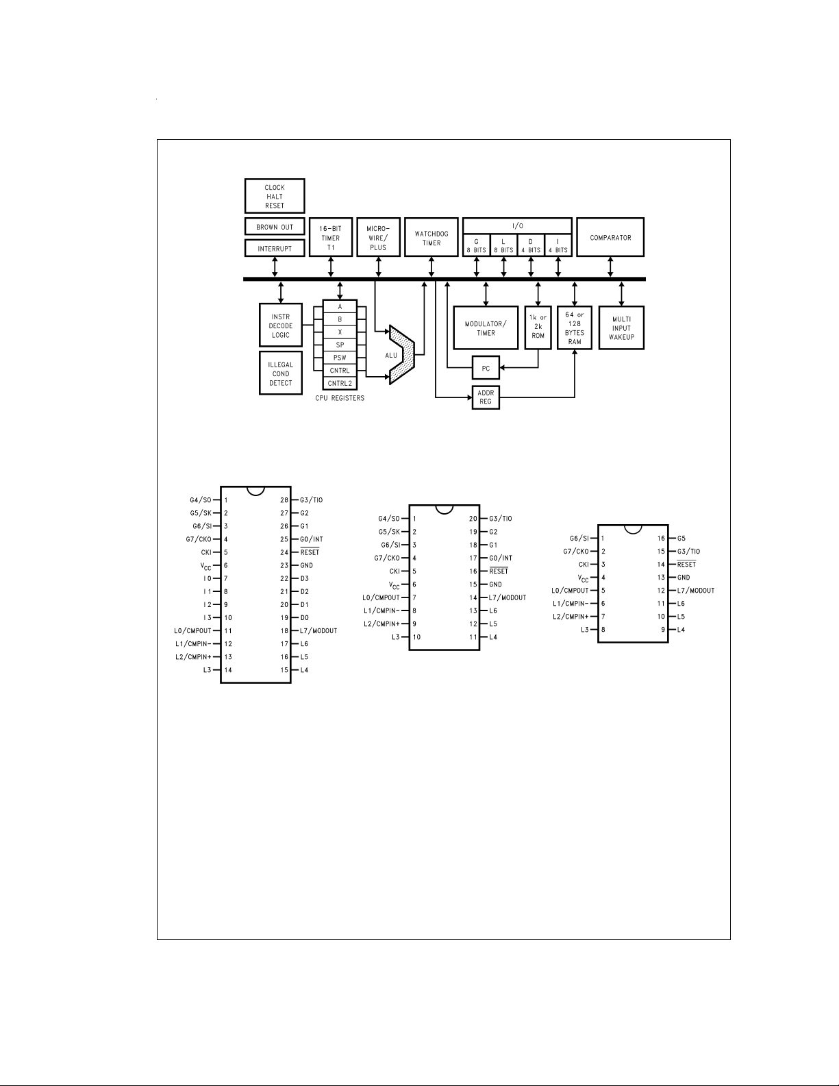
Block Diagram
Connection Diagrams
DS011208-1
2k ROM and 128 Bytes RAM for COP840CJ
FIGURE 1. Block Diagram
DS011208-3
Top View
Order Number COPCJ820-XXX/N or
COPCJ820-XXX/M,
Order Number COPCJ840-XXX/N or
COPCJ840-XXX/M,
Order Number COPCJ940-XXX/N or
COPCJ940-XXX/M
Order Number COPCJ822-XXX/N or
COPCJ822-XXX/M
Order Number COPCJ842-XXX/N or
COPCJ842-XXX/M
Order Number COPCJ942-XXX/N or
COPCJ942-XXX/M
See NS Package Number N20A or
M20B
See NS Package Number N28B or
M28B
FIGURE 2. Connection Diagrams
www.national.com 2
Top View
DS011208-4
DS011208-5
Top View
Order Number COPCJ823-XXX/WM
See NS Package Number M16B
Connection Diagrams (Continued)
COP820CJ/COP840CJ Pin Assignment
Port Pin Typ. ALT Function 16-Pin 20-Pin 28-Pin
L0 I/O MIWU/CMPOUT 5 7 11
L1 I/O MIWU/CMPIN− 6 8 12
L2 I/O MIWU/CMPIN+ 7 9 13
L3 I/O MIWU 8 10 14
L4 I/O MIWU 9 11 15
L5 I/O MIWU 10 12 16
L6 I/O MIWU 11 13 17
L7 I/O MIWU/MODOUT 12 14 18
G0 I/O INTR 17 25
G1 I/O 18 26
G2 I/O 19 27
G3 I/O TIO 15 20 28
G4 I/O SO 1 1
G5 I/O SK 16 2 2
G6 ISI 133
G7 I CKO 2 4 4
I0 I 7
I1 I 8
I2 I 9
I3 I 10
D0 O 19
D1 O 20
D2 O 21
D3 O 22
V
CC
GND 13 15 23
CKI 3 5 5
RESET
466
14 16 24
www.national.com3
Absolute Maximum Ratings (Note 1)
If Military/Aerospace specified devices are required,
please contact the National Semiconductor Sales Office/
Distributors for availability and specifications.
Supply Voltage (V
Voltage at any Pin −0.3V to V
) 7.0V
CC
CC
+ 0.3V
Total Current into V
pin (Source) 80 mA
CC
Total Current out of GND pin (sink) 80 mA
Storage Temperature Range −65˚C to +150˚C
Note 1:
Absolute maximum ratings indicate limits beyond which damage to
the device may occur.
DC and AC electrical specifications are not ensured when operating the device at absolute maximum ratings.
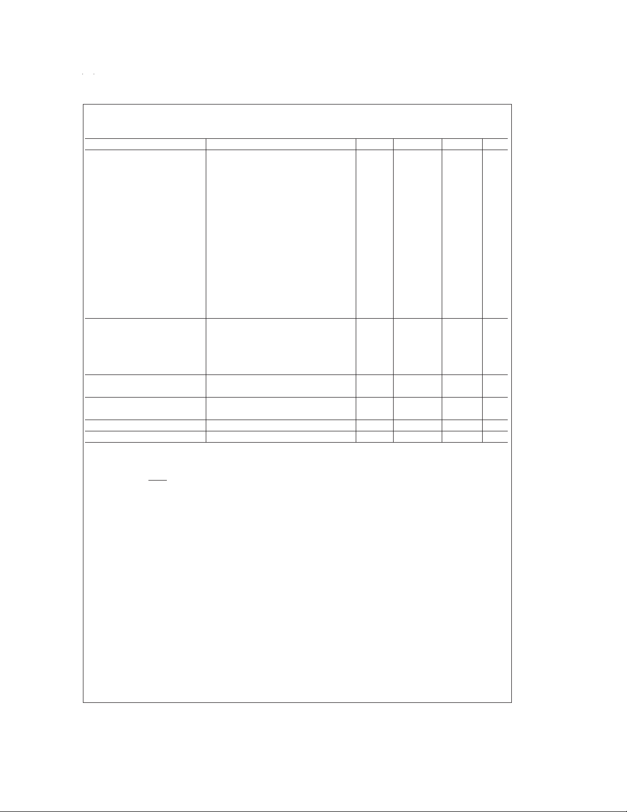
DC Electrical Characteristics
−0˚C ≤ TA≤ + 70˚C for COP94x and −40˚C ≤ TA≤ +85˚C for all others
Parameter Conditions Min Typ Max Units
Operating Voltage Brown Out Disabled 2.5 6.0 V
COP94xCJ Brown Out Disabled 2.5 4.5 V
COP94xCJH Brown Out Disabled 4.5 6.0 V
Power Supply Ripple 1 (Note 2) Peak to Peak 0.1 V
Supply Current (Note 3)
CKI=10 MHz V
CKI=4 MHz V
CKI=4 MHz V
CKI=1 MHz V
HALT Current with Brown Out
Disabled (Note 4)
HALT Current with Brown Out
Enabled
=
6V, tc=1 µs 6.0 mA
CC
=
6V, tc=2.5 µs 3.5 mA
CC
=
4.0V, tc=2.5 µs 2.0 mA
CC
=
4.0V, tc=10 µs 1.5 mA
CC
=
V
6V, CKI=0 MHz
CC
=
V
6V, CKI=0 MHz
CC
<
110µA
<
50 110 µA
COP840CJ Supply Current (Note
3)
=
CKI=10 MHz, R = 2.2k V
CKI=4 MHz, R = 4.7k V
CKI=4 MHz, R = 4.7k V
CKI=1 MHz, R = 20k V
HALT Current with Brown Out
Disabled
HALT Current with Brown Out
Enabled
Brown Out Trip Level (Brown Out
Enabled)
COP840CJ Brown Out Trip Level
6V, tc=1 µs 8.0 mA
CC
=
6V, tc=2.5 µs 6.0 mA
CC
=
4.5V, tc=2.5 µs 2.5 mA
CC
=
4.5V, tc=10 µs 1.5 mA
CC
=
V
6V, CKI=0 MHz
CC
=
V
6V, CKI=0 MHz
CC
<
2.2 8 µA
<
50 100 µA
1.8 3.1 4.2 V
1.9 3.1 3.9 V
(Brown Out Enabled)
INPUT LEVELS (V
IH,VIL
)
Reset, CKI:
Logic High 0.8 V
CC
Logic Low 0.2 V
All Other Inputs
Logic High 0.7 V
CC
Logic Low 0.2 V
Hi-Z Input Leakage V
Input Pullup Current V
=
6.0V −2 +2 µA
CC
=
6.0V, V
CC
=
0V −40 −250 µA
IN
L- and G-Port Hysteresis (Note 6) COP840CJ
0.05 V
CC
0.35 V
CC
CC
CC
CC
V
V
V
V
V
V
www.national.com 4
DC Electrical Characteristics (Continued)
−0˚C ≤ TA≤ + 70˚C for COP94x and −40˚C ≤ TA≤ +85˚C for all others
Parameter Conditions Min Typ Max Units
Output Current Levels
D Outputs:
Source V
Sink V
L4–L7 Output Sink V
=
4.5V, V
CC
=
V
2.5V, V
CC
=
4.5V, V
CC
=
V
2.5V, V
CC
=
4.5V, V
CC
All Others
Source (Weak Pull-up Mode) V
Source (Push-pull Mode) V
Sink (Push-pull Mode) V
=
4.5V, V
CC
=
V
2.5V, V
CC
=
4.5V, V
CC
=
V
2.5V, V
CC
=
4.5V, V
CC
=
V
2.5V, V
CC
TRI-STATE Leakage −2.0 +2.0 µA
Allowable Sink/Source
Current Per Pin
D Outputs 15 mA
L4–L7 (Sink) 20 mA
All Others 3mA
Maximum Input Current Room Temperature
without Latchup (Note 5)
RAM Retention Voltage, V
r
500 ns Rise and 2.0 V
Fall Time (Min)
Input Capacitance 7pF
Load Capacitance on D2 1000 pF
Note 2: Rate of voltage change must be less than 10 V/mS.
Note 3: Supply current is measured after running 2000 cycles with a square wave CKI input, CKO open, inputs at rails and outputs open.
Note 4: The HALT mode will stop CKI from oscillating in the RC and crystal configurations. HALT test conditions: L, and G0..G5 ports configured as outputs and set
high. The D port set to zero. All inputs tied to V
Note 5: Pins G6 and RESET are designed with a high voltage input network. These pins allow input voltages greater than V
to VCCwhen biased at voltages greaterthanVCC(the pins do not havesourcecurrentwhenbiasedata voltage below VCC). The effective resistance to VCCis 750Ω
(typical). These two pins will not latch up. The voltage at the pins must be limited to less than 14V.
. The comparator and the Brown Out circuits are disabled.
CC
=
3.8V −0.4 mA
OH
=
1.8V −0.2 mA
OH
=
1.0V 10 mA
OL
=
0.4V 2 mA
OH
=
2.5V 15 mA
OL
=
3.2V −10 −110 µA
OH
=
1.8V −2.5 −33 µA
OH
=
3.8V −0.4 mA
OH
=
1.8V −0.2 mA
OH
=
0.4V 1.6 mA
OL
=
0.4V 0.7 mA
OL
±
and the pins will have sink current
CC
100 mA
www.national.com5
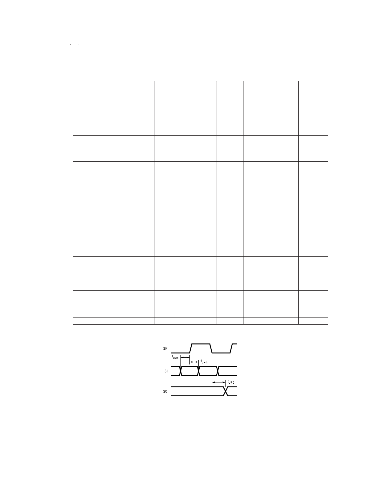
AC Electrical Characteristics
−40˚C ≤ TA≤ +85˚C unless otherwise specified
Parameter Conditions Min Typ Max Units
Instruction Cycle Time (tc)
Crystal/Resonator 4.5V ≤ V
2.5V ≤ V
R/C Oscillator 4.5V ≤ V
COP840CJ 2 DC µs
2.5V ≤ V
COP840CJ 5 DC µs
V
Rise Time when Using Brown
CC
Out
V
CC
Frequency at Brown Out Reset 4 MHz
CKI Frequency For Modular Output 4 MHz
CKI Clock Duty Cycle (Note 6) fr=Max 40 60
Rise Time (Note 6) fr=10 MHz ext. Clock 12 ns
Fall Time (Note 6) fr=10 MHz ext. Clock 8 ns
Inputs
t
Setup
4.5V ≤ VCC≤ 6.0V 200 ns
2.5V ≤ V
t
Hold
4.5V ≤ VCC≤ 6.0V 60 ns
2.5V ≤ V
Output Propagation Delay R
t
PD1,tPD0
L
SO, SK 4.5V ≤ VCC≤ 6.0V 0.7 µs
2.5V ≤ V
All Others 4.5V ≤ V
2.5V ≤ V
Input Pulse Width
Interrupt Input High Time 1 tc
Interrupt Input Low Time 1 tc
Timer Input High Time 1 tc
Timer Input Low Time 1 tc
MICROWIRE Setup Time (t
MICROWIRE Hold Time (t
)20ns
µWS
)56ns
µWH
MICROWIRE Output 220 ns
Propagation Delay (t
µPD
)
Reset Pulse Width 1.0 µs
Note 6: Parameter characterized but not production tested.
≤ 6.0V 1 DC µs
CC
≤ 4.5V 2.5 DC µs
CC
≤ 6.0V 3 DC µs
CC
≤ 4.5V 7.5 DC µs
CC
=
0V to 6V 50 µs
≤ 4.5V 500 ns
CC
≤ 4.5V 150 ns
CC
=
2.2k, CL=100 pF
≤ 4.5V 1.75 µs
CC
≤ 6.0V 1 µs
CC
≤ 4.5V 5 µs
CC
%
FIGURE 3. MICROWIRE/PLUS Timing
www.national.com 6
DS011208-2
Comparator DC and AC Characteristics
4V ≤ VCC≤ 6V, −40˚C ≤ TA≤ + 85˚C (Note 7)
Parameters Conditions Min Type Max Units
<
<
V
Input Offset Voltage 0.4V
IN
VCC− 1.5V
Input Common Mode Voltage Range 0.4 V
±
10
±
25 mV
− 1.5 V
CC
Voltage Gain 300k V/V
DC Supply Current (when enabled) V
=
6.0V 250 µA
CC
Response Time 100 mV Overdrive 60 100 140 ns
500 mV Overdrive 80 125 165 ns
1000 mV Overdrive 135 215 300 ns
Note 7: For comparator output current characteristics see L-Port specs.
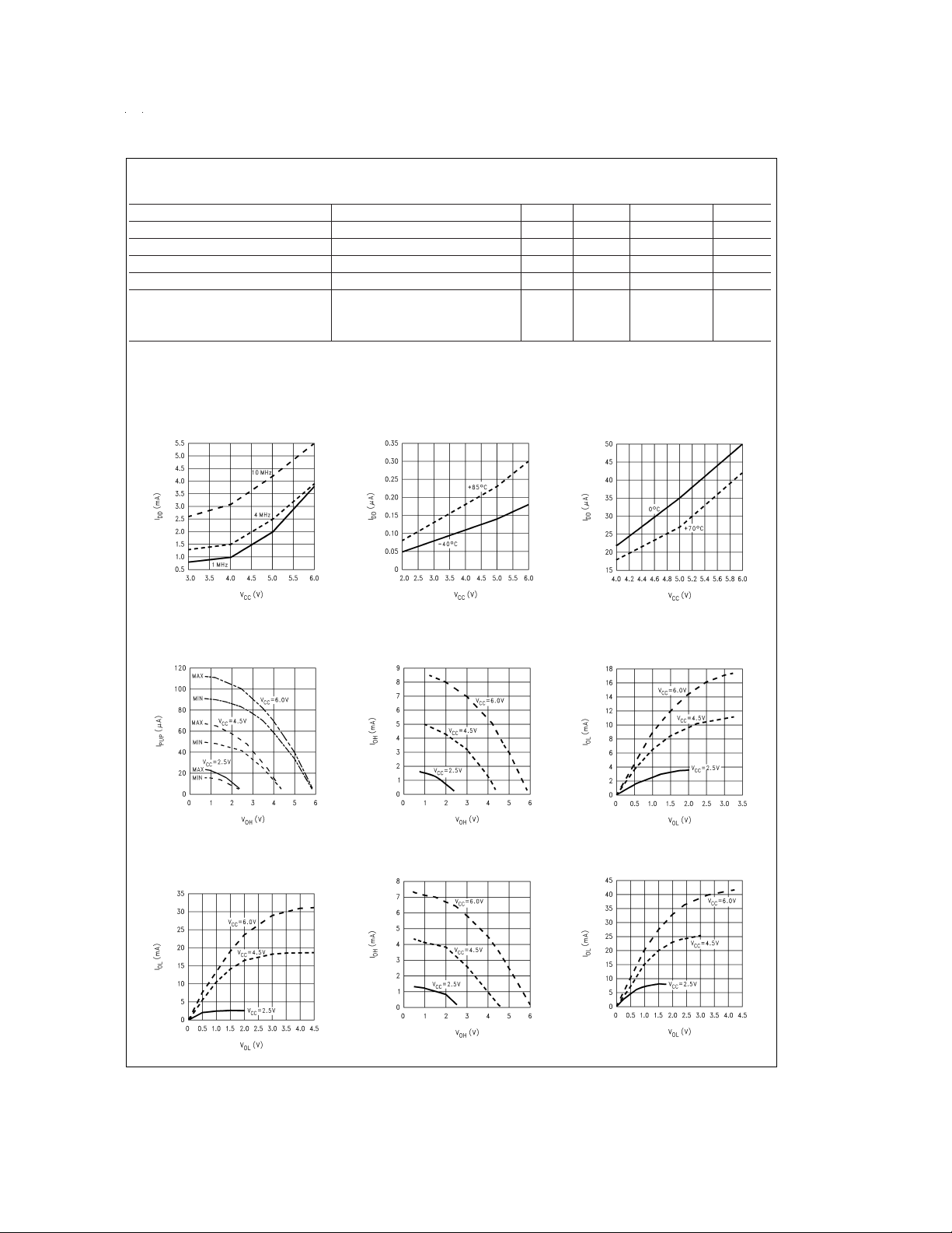
Typical Performance Characteristics for COP820CJ
Dynamic— IDDvs V
(Crystal Clock Option)
CC
Ports L/G Weak
Pull-Up Source Current
Ports L4–L7
Sink Current
DS011208-32
DS011208-35
Halt— IDDvs V
(Brown Out Disabled)
CC
Ports L/G Push-Pull
Source Current
Port D Source Current
DS011208-33
DS011208-36
Halt— IDDvs V
(Brown Out Enabled)
CC
Ports L/G Push-Pull
Sink Current
Port D Sink Current
DS011208-34
DS011208-37
DS011208-38
DS011208-39
DS011208-40
www.national.com7
Typical Performance Characteristics for COP820CJ (Continued)
Brown Out Voltage
vs Temperature
DS011208-41
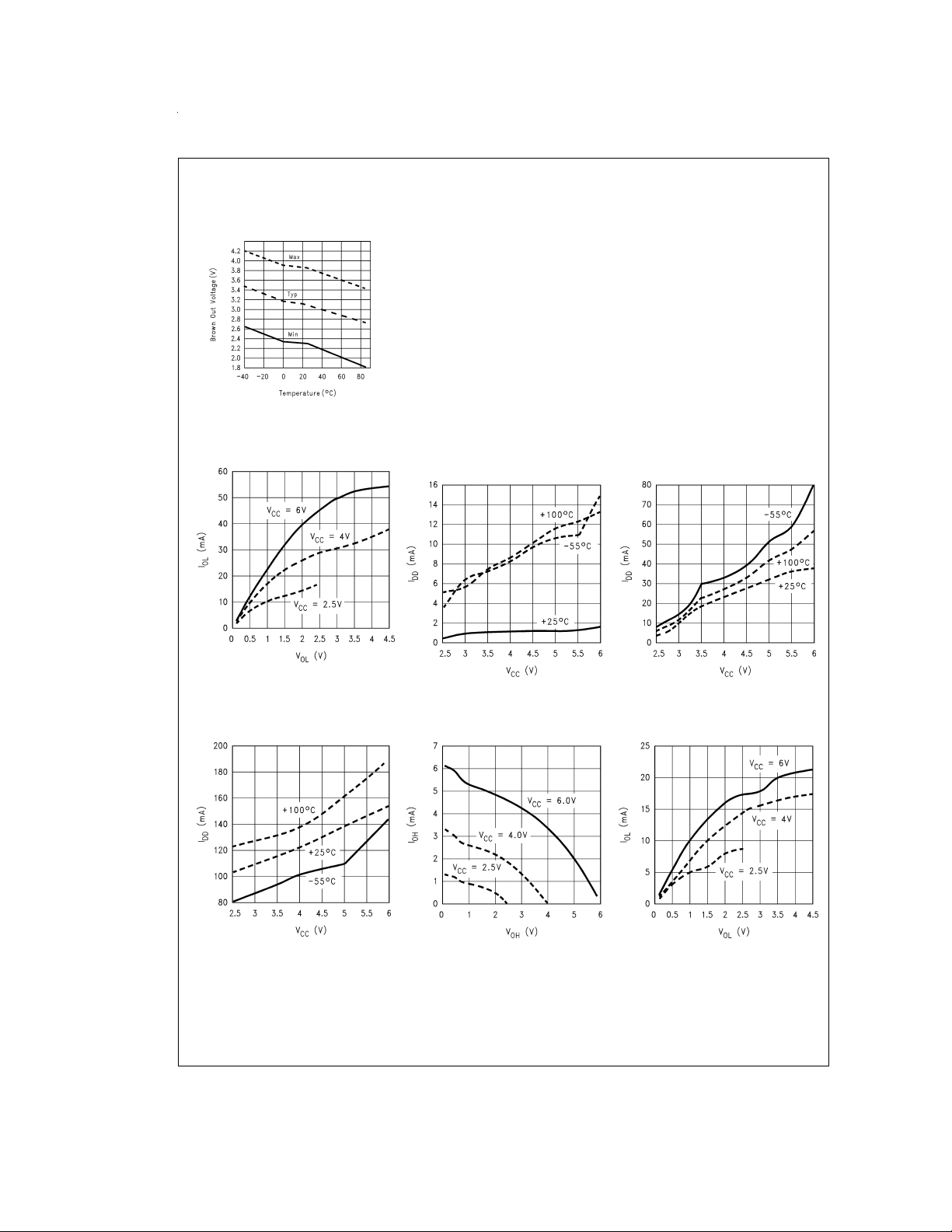
Typical Performance Characteristics for COP840CJ
Port D Sink current
Halt Current with
Comparator Enabled
DS011208-5
Halt Current with
Brown Out Disabled
Ports L/G Push-Pull
Source Current
DS011208-6
Halt Current with
Brown Out Enabled
DS011208-7
Ports L/G Push-Pull
Sink Current
DS011208-8
www.national.com 8
DS011208-9
DS011208-10
Typical Performance Characteristics for COP840CJ (Continued)
Port D Source Current
Brown Out Voltage
vs Temperature
DS011208-11
Port D Sink Current
DS011208-13
DS011208-13
www.national.com9
Pin Description
VCCand GND are the power supply pins.
CKI is the clock input. This can come from an external
source, a R/C generated oscillator or a crystal (in conjunction with CKO). See Oscillator description.
RESET is the master reset input. See Reset description.
PORT I is a 4-bit Hi-Z input port.
PORT L is an 8-bit I/O port.
There are two registers associated with the L port: a data
register and a configuration register. Therefore, each L I/O
bit can be individually configured under software control as
shown below:
Port L Port L Port L
Config. Data Setup
0 0 Hi-Z Input (TRI-STATE)
0 1 Input with Weak Pull-up
1 0 Push-pull Zero Output
1 1 Push-pull One Output
Three data memory address locations are allocated for this
port, one each for data register [00D0], configuration register
[00D1] and the input pins [00D2].
Port L has the following alternate features:
L7 MIWU or MODOUT (high sink current capability)
L6 MIWU (high sink current capability)
L5 MIWU (high sink current capability)
L4 MIWU (high sink current capability)
L3 MIWU
L2 MIWU or CMPIN+
L1 MIWU or CMPIN−
L0 MIWU or CMPOUT
The selection of alternate Port L functions is done through
registers WKEN [00C9] to enable MIWU and CNTRL2
[00CC] to enable comparator and modulator.
All eight L-pins have Schmitt Triggers on their inputs.
PORT G is an 8-bit port with 6 I/O pins (G0–G5) and 2 input
pins (G6, G7).
All eight G-pins have Schmitt Triggers on the inputs.
There are two registers associated with the G port: a data
register and a configuration register. Therefore each G port
bit can be individually configured under software control as
shown below:
Port G Port G Port G
Config. Data Setup
0 0 Hi-Z Input (TRI-STATE)
0 1 Input with Weak Pull-up
1 0 Push-pull Zero Output
1 1 Push-pull One Output
Three data memory address locations are allocated for this
port, one for data register [00D4], one for configuration register [00D5] and one for the input pins [00D6]. Since G6 and
G7 are Hi-Z input only pins, any attempt by the user to configure them as outputs by writing a one to the configuration
register will be disregarded. Reading the G6 and G7 configuration bits will return zeros. Note that the device will be
placed in the Halt mode by writing a “1” to the G7 data bit.
Six pins of Port G have alternate features:
G7 CKO crystal oscillator output (selected by mask option)
or HALT restart input/general purpose input (if clock
option is R/C or external clock)
G6 SI (MICROWIRE serial data input)
G5 SK (MICROWIRE clock I/O)
G4 SO (MICROWIRE serial data output)
G3 TIO (timer/counter input/output)
G0 INTR (an external interrupt)
Pins G2 and G1 currently do not have any alternate func-
tions.
The selection of alternate Port G functions are done through
registers PSW [00EF] to enable external interrupt and CNTRL1 [00EE] to select TIO and MICROWIRE operations.
PORT D is a four bit output port that is preset when RESET
goes low. One data memory address location is allocated for
the data register [00DC].
Note: Care must be exercised with the D2 pin operation. At RESET, the ex-
ternal loads on this pin must ensure that the output voltages stay
above 0.8 V
keep the external loading on D2 to less than 1000 pF.
to prevent the chip from entering special modes. Also
CC
Functional Description
The internal architecture is shown in the block diagram. Data
paths are illustrated in simplified form to depict how the various logic elements communicate with each other in implementing the instruction set of the device.
ALU and CPU Registers
The ALU can do an 8-bit addition, subtraction, logical or shift
operations in one cycle time. There are five CPU registers:
A is the 8-bit Accumulator register
PC is the 15-bit Program Counter register
PU is the upper 7 bits of the program counter (PC)
PL is the lower 8 bits of the program counter (PC)
B is the 8-bit address register and can be auto incre-
mented or decremented.
X is the 8-bit alternate address register and can be auto
incremented or decremented.
SP is the 8-bit stack pointer which points to the subroutine
stack (in RAM).
B, X and SP registers are mapped into the on chip RAM. The
B and X registers are used to address the on chip RAM. The
SP register is used to address the stack in RAM during subroutine calls and returns. The SP must be preset by software
upon initialization.
Memory
The memory is separated into two memory spaces: program
and data.
PROGRAM MEMORY
Program memory consists of 1024 x 8 ROM or 2048 x 8
ROM. These bytes of ROM may be instructions or constant
data. The memory is addressed by the 15-bit program
counter (PC). ROM can be indirectly read by the LAID instruction for table lookup.
DATA MEMORY
The data memory address space includes on chip RAM, I/O
and registers. Data memory is addressed directly by the instruction or indirectly through B, X and SP registers. The device has 64 or 128 bytes of RAM. Sixteen bytes of RAM are
www.national.com 10
Memory (Continued)
mapped as “registers”, these can be loaded immediately,
decremented and tested. Three specific registers: X, B, and
SP are mapped into this space, the other registers are available for general usage.
Any bit of data memory can be directly set, reset or tested.
All I/O and registers (exceptA and PC) are memory mapped;
therefore, I/O bits and register bits can be directly and individually set, reset and tested, except the write once only bit
(WDREN, WATCHDOG Reset Enable), and the unused and
read only bits in CNTRL2 and WDREG registers.
Note: RAM contents are undefined upon power-up.
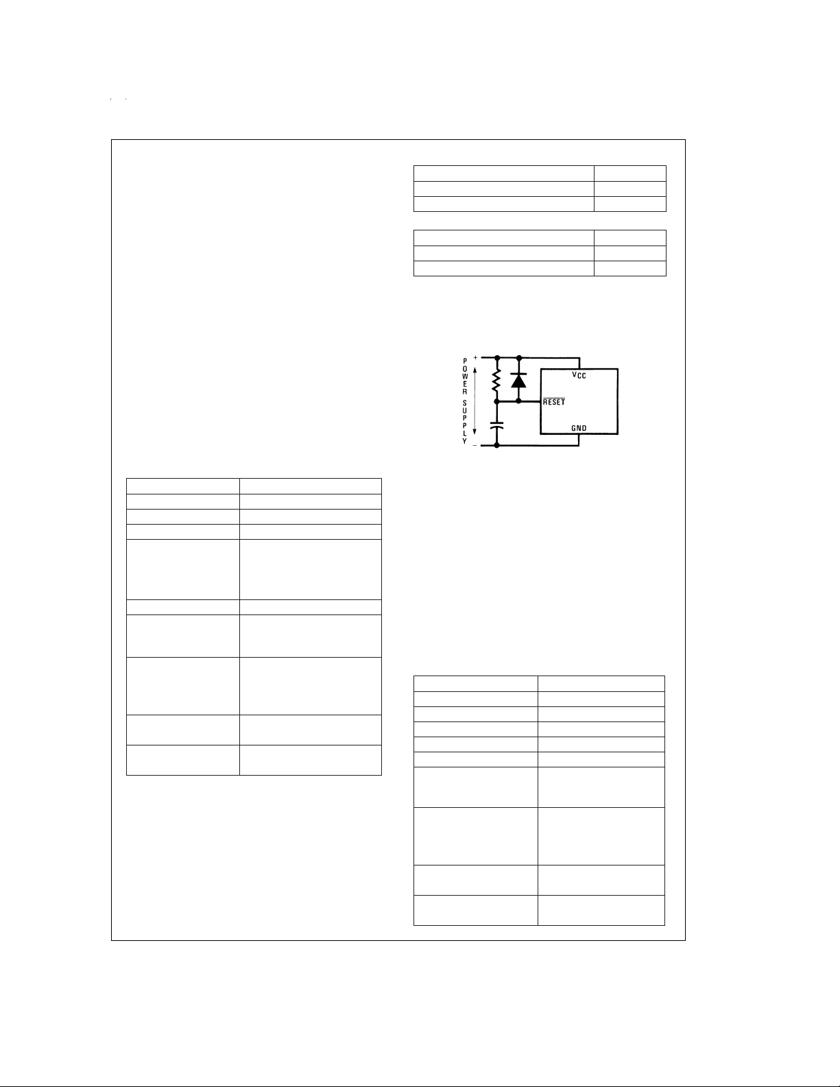
Reset
EXTERNAL RESET
The RESET input pin when pulled low initializes the
micro-controller.The user must insure that the RESET pin is
held low until V
the clock is stabilized. An R/C circuit with a delay 5x greater
than the power supply rise time is recommended (
The device immediately goes into reset state when the RESET input goes low. When the RESET pin goes high the device comes out of reset state synchronously. The device will
be running within two instruction cycles of the RESET pin going high. The following actions occur upon reset:
Port L TRI-STATE
Port G TRI-STATE
Port D HIGH
PC CLEARED
RAM Contents RANDOM with Power-On-
B, X, SP Same as RAM
PSW, CNTRL1,
CNTRL2
and WDREG Reg. CLEARED
Multi-Input Wakeup
Reg.
WKEDG, WKEN CLEARED
WKPND UNKNOWN
Data and Configuration
Registers forL&G CLEARED
WATCHDOG Timer Prescaler/Counter each
The device comes out of the HALT mode when the RESET
pin is pulled low. In this case, the user has to ensure that the
RESET signal is low long enough to allow the oscillator to restart. An internal 256 t
with the two pin crystal oscillator. When the device comes
out of the HALT mode through Multi-Input Wakeup, this delay allows the oscillator to stabilize.
The following additional actions occur after the device
comes out of the HALT mode through the RESET pin.
is within the specified voltage range and
CC
Figure 4
Reset
UNAFFECTED with external
Reset (power already applied)
loaded with FF
delay is normally used in conjunction
c
If a two pin crystal/resonator oscillator is being used:
RAM Contents UNCHANGED
Timer T1 and A Contents UNKNOWN
WATCHDOG Timer Prescaler/Counter ALTERED
If the external or RC Clock option is being used:
RAM Contents UNCHANGED
Timer T1 and A Contents UNCHANGED
WATCHDOG Timer Prescaler/Counter ALTERED
The external RESET takes priority over the Brown Out Reset.
Note: If the RESET pin is pulled low while Brown Out occurs (Brown Out cir-
cuit has detected Brown Out condition), the external reset will not occur until the Brown Out condition is removed. External reset has priority only if V
is greater than the Brown Out voltage.
CC
).
RC>5 x Power Supply Rise Time
FIGURE 4. Recommended Reset Circuit
WATCHDOG RESET
With WATCHDOG enabled, the WATCHDOG logic resets
the device if the user program does not service the WATCHDOG timer within the selected service window. The WATCHDOG reset does not disable the WATCHDOG. Upon
WATCHDOG reset, the WATCHDOGPrescaler and Counter
are each initialized with FF Hex.
The following actions occur upon WATCHDOGreset that are
different from external reset.
WDREN WATCHDOG Reset Enable bit UNCHANGED
WDUDFWATCHDOG Underflow bitUNCHANGED
Additional initialization actions that occur as a result of
WATCHDOG reset are as follows:
Port L TRI-STATE
Port G TRI-STATE
Port D HIGH
PC CLEARED
RAM Contents UNCHANGED/RANDOM
B, X, SP UNCHANGED
PSW, CNTRL1 and
CLEARED
CNTRL2 (except WDUDF
Bit) Registers
Multi-Input Wakeup
Registers
WKEDG, WKEN CLEARED
WKPND UNKNOWN
Data and Configuration
Registers forL&G CLEARED
WATCHDOG Timer Prescalar/Counter
each loaded with FF
DS011208-5
www.national.com11

Reset (Continued)
BROWN OUT RESET
The on-board Brown Out protection circuit resets the device
when the operating voltage (V
Out voltage. The device is held in reset when V
low the Brown Out Voltage.The device will remain in RESET
as long as V
will resume execution if V
is below the Brown Out Voltage. The Device
CC
age. If a two pin crystal/resonator clock option is selected,
the Brown Out reset will trigger a 256tc delay. This delay allows the oscillator to stabilize before the device exits the reset state. The delay is not used if the clock option is either
R/C or external clock. The contents of data registers and
RAM are unknown following a Brown Out reset. The external
reset takes priority over Brown Out Reset and will deactivate
the 256 t
takes priority over the WATCHDOG reset.
cycles delay if in progress. The Brown Out reset
c
The following actions occur as a result of Brown Out reset:
Port L TRI-STATE
Port G TRI-STATE
Port D HIGH
PC CLEARED
RAM Contents RANDOM
B, X, SP UNKNOWN
PSW, CNTRL1, CNTRL2
and WDREG Registers CLEARED
Multi-Input Wakeup Registers
WKEDG, WKEN CLEARED
WKPND UNKNOWN
Data and Configuration
Registers forL&G CLEARED
WATCHDOG Timer Prescalar/Counter each
Timer T1 and Accumulator Unknown data after
Note 8: The development system will detect the BROWN OUT RESET externally and will force the RESET pin low. The Development System does not
emulate the 256tc delay.
Brown Out Detection
An on-board detection circuit monitors the operating voltage
(V
) and compares it with the minimum operating voltage
CC
specified. The Brown Out circuit is designed to reset the device if the operating voltage is below the Brown Out voltage
(between 1.8V to 4.2V at −40˚C to +85˚C). The Minimum operating voltage for the device is 2.5V with Brown Out disabled, but with BROWN OUT enabled the device is guaranteed to operate properly down to minimum Brown Out
R1 R2 C1 C2 CKI Freq.
(kΩ)(MΩ) (pF) (pF) (MHz)
0 1 30 30–36 10 V
0 1 30 30–36 4 V
5.6 1 100/200 100–156 0.455 V
) is lower than the Brown
CC
rises above the Brown Out Volt-
CC
stays be-
CC
loaded with FF
coming out of the HALT
(through Brown Out
Reset) with any Clock
option
TABLE 1. Crystal Oscillator Configuration
voltage (Max frequency 4 MHz), For temperature range of
0˚C to 70˚C the Brown Out voltage is expected to be between 1.9V to 3.9V. The circuit can be enabled or disabled
by Brown Out mask option. If the device is intended to operate at lower V
the Brown Out circuit should be disabled by the mask option.
(lower than Brown Out voltage VBO max),
CC
The Brown Out circuit may be used as a power-up reset provided the power supply rise time is slower than 50 µs (0V to
6.0V). Brown Out should not be used at frequencies over 4
MHz (COP840CJ).
Note: Brown Out Circuit is active in HALT mode (with the Brown Out mask
option selected).
Oscillator Circuits
EXTERNAL OSCILLATOR
CKI can be driven by an external clock signal provided it
meets the specified duty cycle, rise and fall times, and input
levels. G7/CKO is available as a general purpose input G7
and/or Halt control.
CRYSTAL OSCILLATOR
By selecting G7/CKO as a clock output, CKI and G7/CKO
can be connected to create a crystal controlled oscillator.
Table 1
shows the component values required for various
standard crystal values.
R/C OSCILLATOR (COP820CJ)
For COP820CJ, selecting CKI as a single pin oscillator, CKI
can make a R/C oscillator. G7/CKO is available as a general
purpose input and/or HALT control.
Table 2
shows variation
in the oscillator frequencies as functions of the component
(R and C) values.
DS011208-15
FIGURE 5. Clock Oscillator Configurations
Conditions
=
5V
CC
=
5V
CC
=
5V
CC
www.national.com 12

Reset (Continued)
TABLE 2. R/C Oscillator Configuration (Part-To-Part Variation)
R C CK1 Freq. Instr. Cycle
(kΩ) (pF) (MHz) (µs)
3.3 82 2.2 to 2.7 3.7 to 4.6 V
5.6 100 1.1 to 1.3 7.4 to 9.0 V
6.8 100 0.9 to 1.1 8.8 to 10.8 V
R/C OSCILLATOR (COP840CJ)
For COP840CJ, selecting the R/C oscillator option makes a
R/C oscillator when connecting a resistor from the CKI pin to
V . The capacitor is on-chip. The G7/CKO pin is available as
a general purpose input G7 and/or Halt control. Adding an
external capacitor will jeopardize the clock frequency tolerance and increase EMI emissions.
frequency for the different resistor values.
TABLE 3. RC Oscillator Configuration (Part-To-Part Variation)
R(kΩ) CK1 Freq. (MHz) Temperature V
2.2 7.0±15
4.7 4.2
20.0 7.1
Note 9: The resistance level is calculated with a total of 5.3 pF capacitance added from the printed circuit board. It is important to take this into account when figuring
the clock frequency.
%
±
%
10
±
%
10
-40˚C to +85˚C 4.5V to 5.5V
-40˚C to +85˚C 4.5V to 5.5V
-40˚C to +85˚C 4.5V to 5.5V
HALT Mode
The device is a fully static device. The device enters the
HALTmode by writing a one to the G7 bit of the G data register. Once in the HALT mode, the internal circuitry does not
receive any clock signal and is therefore frozen in the exact
state it was in when halted. In this mode, the chip will only
draw leakage current (output current and DC current due to
the Brown Out circuit if Brown Out is enabled).
The device supports four different methods of exiting the
HALT mode. The first method is with a low to high transition
on the CKO (G7) pin. This method precludes the use of the
crystal clock configuration (since CKO is a dedicated output). It may be used either with an RC clock configuration or
an external clock configuration. The second method of exiting the HALT mode is with the multi-Input Wakeup feature on
the L port. The third method of exiting the HALT mode is by
pulling the RESET input low. The fourth method is with the
operating voltage going below Brown Out voltage (if Brown
Out is enabled by mask option).
If the two pin crystal/resonator oscillator is being used and
Multi-Input Wakeup or Brown Out causes the device to exit
the HALT mode, the WAKEUP signal does not allow the chip
to start running immediately since crystal oscillators have a
delayed start up time to reach full amplitude and freuqency
stability.The WATCHDOG timer (consisting of an 8-bit prescaler followed by an 8-bit counter) is used to generate a fixed
delay of 256tc to ensure that the oscillator has indeed stabilized before allowing instruction execution. In this case, upon
detecting a valid WAKEUP signal only the oscillator circuitry
is enabled. The WATCHDOG Counter and Prescaler are
each loaded with a value of FF Hex. The WATCHDOG prescaler is clocked with the t
derived by dividing the oscillator clock down by a factor of
instruction cycle. (The tcclock is
c
10). The Schmitt trigger following the CKI inverter on the chip
ensures that the WATCHDOGtimer is clocked only when the
oscillator has a sufficiently large amplitude to meet the
Schmitt trigger specs. This Schmitt trigger is not part of the
oscillator closed loop. The start-up timeout from the WATCHDOG timer enables the clock signals to be routed to the rest
of the chip. The delay is not activated when the device
comes out of HALT mode through RESET pin. Also, if the
clock option is either RC or External clock, the delay is not
used, but the WATCHDOG Prescaler/Counter contents are
changed. The Development System will not emulate the
256tc delay.
The RESET pin or Brown Out will cause the device to reset
and start executing from address X’0000. A low to high transition on the G7 pin (if single pin oscillator is used) or
Multi-Input Wakeup will cause the device to start executing
from the address following the HALT instruction.
When RESET pin is used to exit the device from the HALT
mode and the two pin crystal/resonator (CKI/CKO) clock option is selected, the contents of the Accumulator and the
Timer T1 are undetermined following the reset. All other information except the WATCHDOG Prescaler/Counter contents is retained until continuing. If the device comes out of
the HALT mode through Brown Out reset, the contents of
data registers and RAM are unknown following the reset. All
information except the WATCHDOGPrescaler/Counter contents is retained if the device exits the HALT mode through
G7 pin or Multi-Input Wakeup.
G7 is the HALT-restartpin, but it can still be used as an input.
If the device is not halted, G7 can be used as a general purpose input.
If the Brown Out Enable mask option is selected, the Brown
Out circuit remains active during the HALTmode causing additional current to be drawn.
Note: To allow clock resynchronization, it is necessary to program two NOP’s
immediately after the device comes out of the HALT mode. The user
must program two NOP’s following the “enter HALT mode” (set G7
data bit) instruction.
MICROWIRE/PLUS
MICROWIRE/PLUS is a serial synchronous bidirectional
communications interface. The MICROWIRE/PLUS capability enables the device to interface with any of National Semiconductor’s MICROWIRE peripherals (i.e. A/D converters,
display drivers, EEPROMS, etc.) and with other microcontrollers which support the MICROWIRE/PLUS interface. It
consists of an 8-bit serial shift register (SIO) with serial data
Conditions
=
5V
CC
=
5V
CC
=
5V
CC
Table 3
CC
shows the clock
www.national.com13

Reset (Continued)
input (SI), serial data output (SO) and serial shift clock (SK).
Figure 6
shows the block diagram of the MICROWIRE/PLUS
interface.
DS011208-8
FIGURE 6. MICROWIRE/PLUS Block Diagram
The shift clock can be selected from either an internal source
or an external source. Operating the MICROWIRE/PLUS interface with the internal clock source is called the Master
mode of operation. Operating the MICROWIRE/PLUS interface with an external shift clock is called the Slave mode of
operation.
The CNTRL register is used to configure and control the
MICROWIRE/PLUS mode. To use the MICROWIRE/PLUS ,
the MSEL bit in the CNTRL register is set to one. The SK
clock rate is selected by the two bits, SL0 and SL1, in the
CNTRL register.
may be selected.
Table4
details the different clock rates that
TABLE 4.
SL1 SL0 SK Cycle Time
00 2t
01 4t
1x 8t
where,
is the instruction cycle time.
t
c
c
c
c
MICROWIRE/PLUS OPERATION
Setting the BUSY bit in the PSW register causes the
MICROWIRE/PLUS arrangement to start shifting the data. It
gets reset when eight data bits have been shifted. The user
may reset the BUSY bit by software to allow less than 8 bits
to shift. The device may enter the MICROWIRE/PLUS mode
either as a Master or as a Slave.
Figure 7
shows how two device microcontrollers and several peripherals may be interconnected using the MICROWIRE/PLUS arrangement.
MASTER MICROWIRE/PLUS OPERATION
In the MICROWIRE/PLUS Master mode of operation the
shift clock (SK) is generated internally by the device. The
MICROWIRE/PLUS Master always initiates all data exchanges (
Figure 7
). The MSEL bit in the CNTRL register
must be set to enable the SO and SK functions on the G
Port. The SO and SK pins must also be selected as outputs
by setting appropriate bits in the Port G configuration register.
Table 5
summarizes the bit settings required for Master
mode of operation.
SLAVE MICROWIRE/PLUS OPERATION
In the MICROWIRE/PLUS Slave mode of operation the SK
clock is generated by an external source. Setting the MSEL
bit in the CNTRL register enables the SO and SK functions
on the G Port. The SK pin must be selected as an input and
the SO pin selected as an output pin by appropriately setting
up the Port G configuration register.
Table5
summarizes the
settings required to enter the Slave mode of operation.
FIGURE 7. MICROWIRE/PLUS Application
www.national.com 14
DS011208-23

Reset (Continued)
The user must set the BUSY flag immediately upon entering
the Slave mode. This will ensure that all data bits sent by the
Master will be shifted properly. After eight clock pulses the
BUSY flag will be cleared and the sequence may be repeated. (See
Figure 7
).
MODE 1. TIMER WITH AUTO-LOAD REGISTER
In this mode of operation, the timer T1 counts down at the instruction cycle rate. Upon underflow the value in the register
R1 gets automatically reloaded into the timer which continues to count down. The timer underflow can be programmed
to interrupt the microcontroller. A bit in the control register
CNTRL enables the TIO (G3) pin to toggle upon timer underflows. This allows the generation of square-wave outputs or
TABLE 5.
G4 G5 G4 G5 G6
Config. Config. Fun. Fun. Fun. Operation
Bit Bit
1 1 SO Int.SKSI MICROWIRE
0 1 TRI-STATE Int.SKSI MICROWIRE
1 0 SO Ext.SKSI MICROWIRE
0 0 TRI-STATE Ext.SKSI MICROWIRE
Master
Master
Slave
Slave
pulse width modulated outputs under software control
(
Figure 8
).
MODE 2. EXTERNAL COUNTER
In this mode, the timer T1 becomes a 16-bit external event
counter. The counter counts down upon an edge on the TIO
pin. Control bits in the register CNTRL program the counter
to decrement either on a positive edge or on a negative
edge. Upon underflow the contents of the register R1 are automatically copied into the counter. The underflow can also
be programmed to generate an interrupt (
Timer/Counter
The device has a powerful 16-bit timer with an associated
16-bit register enabling it to perform extensive timer functions. The timer T1 and its register R1 are each organized as
two 8-bit read/write registers. Control bits in the register CNTRL allow the timer to be started and stopped under software control. The timer-register pair can be operated in one
of three possible modes.
ating modes and their requisite control settings.
CNTRL Timer
Bits Operation Mode T Interrupt Counts
765 On
0 0 0 External Counter w/Auto-Load Reg. Timer Underflow TIO Pos. Edge
0 0 1 External Counter w/Auto-Load Reg. Timer Underflow TIO Neg. Edge
0 1 0 Not Allowed Not Allowed Not Allowed
0 1 1 Not Allowed Not Allowed Not Allowed
1 0 0 Timer w/Auto-Load Reg. Timer Underflow t
1 0 1 Timer w/Auto-Load Reg./Toggle TIO Out Timer Underflow t
1 1 0 Timer w/Capture Register TIO Pos. Edge t
1 1 1 Timer w/Capture Register TIO Neg. Edge t
Table 6
details various timer oper-
FIGURE 8. Timer/Counter Auto
Reload Mode Block Diagram
TABLE 6. Timer Operating Modes
c
c
c
c
Figure 9
DS011208-24
).
www.national.com15

Timer/Counter (Continued)
FIGURE 9. Timer in External Event Counter Mode
MODE 3. TIMER WITH CAPTURE REGISTER
Timer T1 can be used to precisely measure external frequencies or events in this mode of operation. The timer T1
counts down at the instruction cycle rate. Upon the occurrence of a specified edge on the TIO pin the contents of the
timer T1 are copied into the register R1. Bits in the control
register CNTRL allow the trigger edge to be specified either
as a positive edge or as a negative edge. In this mode the
user can elect to be interrupted on the specified trigger edge
Figure 10
(
).
DS011208-29
DS011208-26
FIGURE 11. Timer Application
DS011208-25
FIGURE 10. Timer Capture Mode Block Diagram
TIMER PWM APPLICATION
Figure 11
shows how a minimal component D/A converter
can be built out of the Timer-Register pair in the Auto-Reload
mode. The timer is placed in the “Timer with auto reload”
mode and the TIO pin is selected as the timer output. At the
outset the TIO pin is set high, the timer T1 holds the on time
and the register R1 holds the signal off time. Setting TRUN
bit starts the timer which counts down at the instruction cycle
rate. The underflow toggles the TIO output and copies the off
time into the timer, which continues to run. By alternately
loading in the on time and the off time at each successive interrupt a PWM frequency can be easily generated.
www.national.com 16
WATCHDOG
The device has an on-board 8-bit WATCHDOG timer. The
timer contains an 8-bit READ/WRITE down counter clocked
by an 8-bit prescaler. Under software control the timer can
be dedicated for the WATCHDOGor used as a general purpose counter.
diagram.
MODE 1: WATCHDOG TIMER
The WATCHDOG is designed to detect user programs getting stuck in infinite loops resulting in loss of program control
or “runaway” programs. The WATCHDOGcan be enabled or
disabled (only once) after the device is reset as a result of
brown out reset or external reset. On power-up the WATCHDOG is disabled. The WATCHDOG is enabled by writing a
“1” to WDREN bit (resides in WDREG register). Once enabled, the user program should write periodically into the
8-bit counter before the counter underflows. The 8-bit
counter (WDCNT) is memory mapped at address 0CE Hex.
The counter is loaded with n-1 to get n counts. The counter
underflow resets the device, but does not disable the
WATCHDOG. Loading the 8-bit counter initializes the prescaler with FF Hex and starts the prescaler/counter.Prescaler
and counter are stopped upon counter underflow. Prescaler
and counter are each loaded with FF Hex when the device
goes into the HALT mode. The prescaler is used for crystal/
resonator start-up when the device exits the HALT mode
through Multi-Input Wakeup. In this case, the prescaler/
counter contents are changed.
Figure 12
shows the WATCHDOG timer block

WATCHDOG (Continued)
MODE 2: TIMER
In this mode, the prescaler/counter is used as a timer by
keeping the WDREN (WATCHDOG reset enable) bit at 0.
The counter underflow sets the WDUDF (underflow) bit and
the underflow does not reset the device. Loading the 8-bit
counter (load n-1 for n counts) sets the WDTEN bit (WATCHDOG Timer Enable) to “1”, loads the prescaler with FF, and
TABLE 7. WATCHDOG Control/Status
HALT WD EXT/BOR Counter
Parameter Mode Reset Reset Load
8-Bit Prescaler FF FF FF FF
8-Bit WD Counter FF FF FF User Value
WDREN Bit Unchanged Unchanged 0 No Effect
WDUDF Bit 0 Unchanged 0 0
WDTEN Signal Unchanged 0 0 1
Note 10: BOR is Brown Out Reset.
starts the timer. The counter underflow stops the timer. The
WDTEN bit serves as a start bit for the WATCHDOG timer.
This bit is set when the 8-bit counter is loaded by the user
program. The load could be as a result of WATCHDOG service (WATCHDOG timer dedicated for WATCHDOG function) or write to the counter (WATCHDOG timer used as a
general purpose counter). The bit is cleared upon Brown Out
reset, WATCHDOG reset or external reset. The bit is not
memory mapped and is transparent to the user program.
(Note 10)
CONTROL/STATUS BITS
WDUDF: WATCHDOG Timer Underflow Bit
This bit resides in the CNTRL2 Register. The bit is set when
the WATCHDOGtimer underflows. The underflow resets the
device if the WATCHDOG reset enable bit is set (WDREN
1). Otherwise, WDUDF can be used as the timer underflow
flag. The bit is cleared upon Brown-Out reset, external reset,
load to the 8-bit counter, or going into the HALT mode. It is a
read only bit.
WDREN: WD Reset Enable
WDREN bit resides in a separate register (bit 0 of WDREG).
This bit enables the WATCHDOG timer to generate a reset.
The bit is cleared upon Brown Out reset, or external reset.
The bit under software control can be written to only once
(once written to, the hardware does not allow the bit to be
=
changed during program execution).
WDREN=1 WATCHDOG reset is enabled.
WDREN=0 WATCHDOG reset is disabled.
Table7
shows the impact of Brown Out Reset, WATCHDOG
Reset, and External Reset on the Control/Status bits.
www.national.com17

WATCHDOG (Continued)
FIGURE 12. WATCHDOG Timer Block Diagram
Modulator/Timer
The Modulator/Timer contains an 8-bit counter and an 8-bit
autoreload register (MODRL address 0CF Hex). The
Modulator/Timer has two modes of operation, selected by
the control bit MC3. The Modulator/Timer Control bits MC1,
MC2 and MC3 reside in CNTRL2 Register.
MODE 1: MODULATOR
The Modulator is used to generate high frequency pulses on
the modulator output pin (L7). The L7 pin should be configured as an output. The number of pulses is determined by
the 8-bit down counter. Under software control the modulator
input clock can be either CKI or tC. The t
dividing down the oscillator clock by a factor of 10. Three
control bits (MC1, MC2, and MC3) are used for the
Modulator/Timer output control. When MC2=1 and MC3
1, CKI is used as the modulator input clock. When MC2=0,
and MC3=1, t
user loads the counter with the desired number of counts
is used as the modulator input clock. The
c
(256 max) and sets MC1 to start the counter. The modulator
autoreload register is loaded with n-1 to get n pulses. CKI or
t
pulses are routed to the modulator output (L7) until the
c
counter underflows (
Figure 13
). Upon underflow the hardware resets MC1 and stops the counter. The L7 pin goes low
and stays low until the counter is restarted by the user program. The user program has the responsibility to timeout the
www.national.com 18
clock is derived by
c
=
DS011208-15
low time. Unless the number of counts is changed, the user
program does not have to load the counter each time the
counter is started. The counter can simply be started by setting the MC1 bit. Setting MC1 by software will load the
counter with the value of the autoreload register. The software can reset MC1 to stop the counter.
MODE 2: PWM TIMER
The counter can also be used as a PWM Timer.In this mode,
an 8-bit register is used to serve as an autoreload register
(MODRL).
a. 50%Duty Cycle:
When MC1 is 1 and MC2, MC3 are 0, a 50%duty cycle free
running signal is generated on the L7 output pin (
Figure 14
The L7 pin must be configured as an output pin. In this mode
the 8-bit counter is clocked by tC. Setting the MC1 control bit
by software loads the counter with the value of the autoreload register and starts the counter. The counter underflow
toggles the (L7) output pin. The 50%duty cycle signal will be
continuously generated until MC1 is reset by the user program.
).

Modulator/Timer (Continued)
b. Variable Duty Cycle:
When MC3=0 and MC2=1, a variable duty cycle PWM signal is generated on the L7 output pin. The counter is clocked
by tC. In this mode the 16-bit timer T1 along with the 8-bit
down counter are used to generate a variable duty cycle
PWM signal. The timer T1 underflow sets MC1 which starts
the down counter and it also sets L7 high (L7 should be configured as an output).When the counter underflows the MC1
control bit is reset and the L7 output will go low until the next
timer T1 underflow. Therefore, the width of the output pulse
is controlled by the 8-bit counter and the pulse duration is
controlled by the 16-bit timer T1 (
be configured in “PWM Mode/ToggleTIO Out” (CNTRL1 Bits
7,6,5=101).
Table 8
shows the different operation modes for the
Modulator/Timer.
Figure 15
). Timer T1 must
Internal Data Bus
TABLE 8. Modulator/Timer Modes
Control Bits in Operation Mode
CNTRL2(00CC)
L7 Function
MC3 MC2 MC1
0 0 0 Normal I/O
00150
%
Duty Cycle Mode (Clocked by
)
t
c
0 1 X Variable Duty Cycle Mode (Clocked
by t
) Using Timer 1 Underflow
c
1 0 X Modulator Mode (Clocked by t
1 1 X Modulator Mode (Clocked by CKI)
Note 11: MC1, MC2 and MC3 control bits are cleared upon reset.
)
c
FIGURE 13. Mode 1: Modulator Block Diagram/Output Waveform
DS011208-16
DS011208-17
www.national.com19

Modulator/Timer (Continued)
DS011208-18
FIGURE 14. Mode 2a: 50%Duty Cycle Output
DS011208-19
DS011208-20
FIGURE 15. Mode 2b: Variable Duty Cycle Output
Comparator
The device has one differential comparator. Ports L0–L2 are
used for the comparator. The output of the comparator is
brought out to a pin. Port L has the following assignments:
L0 Comparator output
L1 Comparator negative input
L2 Comparator positive input
THE COMPARATOR STATUS/CONTROL BITS
These bits reside in the CNTRL2 Register (Address 0CC)
CMPEN Enables comparator (“1”=enable)
CMPOE Enables comparator output to pin L0
The Comparator Select/Control bits are cleared on RESET
(the comparator is disabled). To save power the program
should also disable the comparator before the device enters
the HALT mode.
The user program must set up L0, L1 and L2 ports correctly
for comparator Inputs/Output: L1 and L2 need to be configured as inputs and L0 as output. See
(CMPEN=1, CMPOE=X)
(“1”=enable), CMPEN bit must be set to enable
this function. If CMPEN=0, L0 will be 0.
Table 9
.
CMPRD Reads comparator output internally
TABLE 9. Comparator DC and AC Characteristics
4V ≤ VCC≤ 6V, −40˚C ≤ TA≤ + 85˚C (Note 7)
Parameters Conditions Min Type Max Units
<
<
V
Input Offset Voltage 0.4V
IN
VCC− 1.5V
Input Common Mode Voltage Range 0.4 V
±
10
±
25 mV
− 1.5 V
CC
Voltage Gain 300k V/V
DC Supply Current (when enabled) V
=
6.0V 250 µA
CC
Response Time 100 mV Overdrive 60 100 140 ns
500 mV Overdrive 80 125 165 ns
1000 mV Overdrive 135 215 300 ns
Note 12: For comparator output current characteristics see L-Port specs.
www.national.com 20

Multi-Input Wake Up
The Multi-Input Wakeup feature is used to return
(wakeup) the device from the HALT mode.
shows the Multi-Input Wakeup logic.
This feature utilizes the L Port. The user selects which
particular L port bit or combination of L Port bits will cause
the device to exit the HALT mode. Three 8-bit memory
mapped registers, Reg:WKEN, Reg:WKEDG, and Reg:WKPND are used in conjunction with the L port to implement the Multi-Input Wakeup feature.
All three registers Reg:WKEN, Reg:WKPND, and
Reg:WKEDG are read/write registers, and are cleared at
reset, except WKPND. WKPND is unknown on reset.
The user can select whether the trigger condition on the
selected L Port pin is going to be either a positive edge
(low to high transition) or a negative edge (high to low
transition). This selection is made via the Reg:WKEDG,
which is an 8-bit control register with a bit assigned to
each L Port pin. Setting the control bit will select the trigger condition to be a negative edge on that particular L
Port pin. Resetting the bit selects the trigger condition to
be a positive edge. Changing an edge select entails several steps in order to avoid a pseudo Wakeup condition as
a result of the edge change. First, the associated WKEN
bit should be reset, followed by the edge select change in
WKEDG. Next, the associated WKPND bit should be
cleared, followed by the associated WKEN bit being
re-enabled.
An example may serve to clarify this procedure. Suppose
we wish to change the edge select from positive (low going high) to negative (high going low) for L port bit 5,
where bit 5 has previously been enabled for an input. The
program would be as follows:
RBIT 5, WKEN ; Disable MIWU
SBIT 5, WKEDG ; Change edge polarity
RBIT 5, WKPND ; Reset pending flag
SBIT 5, WKEN ; Enable MIWU
If the L port bits have been used as outputs and then
changed to inputs with Multi-Input Wakeup, a safety procedure should also be followed to avoid inherited pseudo
wakeup conditions. After the selected L port bits have
been changed from output to input but before the associated WKEN bits are enabled, the associated edge select
bits in WKEDG should be set or reset for the desired edge
selects, followed by the associated WKPND bits being
cleared. This same procedure should be used following
RESET, since the L port inputs are left floating as a result
of RESET.
The occurrence of the selected trigger condition for
Multi-Input Wakeup is latched into a pending register
called Reg:WKPND. The respective bits of the WKPND
register will be set on the occurrence of the selected trigger edge on the corresponding Port L pin. The user has
the responsibility of clearing these pending flags. Since
the Reg:WKPND is a pending register for the occurrence
of selected wakeup conditions, the device will not enter
the HALT mode if any Wakeup bit is both enabled and
pending. Setting the G7 data bit under this condition will
not allow the device to enter the HALT mode. Consequently, the user has the responsibility of clearing the
pending flags before attempting to enter the HALT mode.
If a crystal oscillator is being used, the Wakeup signal will
not start the chip running immediately since crystal oscillators have a finite start up time. The WATCHDOG timer
Figure 16
prescaler generates a fixed delay to ensure that the oscillator has indeed stabilized before allowing the device to
execute instructions. In this case, upon detecting a valid
Wakeup signal only the oscillator circuitry and the
WATCHDOG timer are enabled. The WATCHDOG timer
prescaler is loaded with a value of FF Hex (256 counts)
and is clocked from the t
clock is derived by dividing down the oscillator clock by a
instruction cycle clock. The t
c
factor of 10. A Schmitt trigger following the CKI on chip inverter ensures that the WATCHDOG timer is clocked only
when the oscillator has a sufficiently large amplitude to
meet the Schmitt trigger specs. This Schmitt trigger is not
part of the oscillator closed loop. The startup timeout from
the WATCHDOG timer enables the clock signals to be
routed to the rest of the chip.
DS011208-27
FIGURE 16. Multi-Input Wakeup Logic
INTERRUPTS
The device has a sophisticated interrupt structure to allow
easy interface to the real world. There are three possible
interrupt sources, as shown below.
— A maskable interrupt on external G0 input (positive or
negative edge sensitive under software control)
— A maskable interrupt on timer carry or timer capture
— A non-maskable software/error interrupt on opcode
zero
INTERRUPT CONTROL
The GIE (global interrupt enable) bit enables the interrupt
function. This is used in conjunction with ENI and ENTI to
select one or both of the interrupt sources. This bit is reset
when interrupt is acknowledged.
ENI and ENTI bits select external and timer interrupts respectively.Thus the user can select either or both sources
to interrupt the microcontroller when GIE is enabled.
IEDG selects the external interrupt edge (0=rising edge,
1=falling edge). The user can get an interrupt on both rising and falling edges by toggling the state of IEDG bit after
each interrupt.
IPND and TPND bits signal which interrupt is pending. After an interrupt is acknowledged, the user can check these
two bits to determine which interrupt is pending. This permits the interrupts to be prioritized under software. The
c
www.national.com21

Multi-Input Wake Up (Continued)
pending flags have to be cleared by the user. Setting the
GIE bit high inside the interrupt subroutine allows nested
interrupts.
The software interrupt does not reset the GIE bit. This
means that the controller can be interrupted by other interrupt sources while servicing the software interrupt.
INTERRUPT PROCESSING
The interrupt, once acknowledged, pushes the program
counter (PC) onto the stack and the stack pointer (SP) is
decremented twice. The Global Interrupt Enable (GIE) bit
is reset to disable further interrupts. The microcontroller
then vectors to the address 00FFH and resumes execution from that address. This process takes 7 cycles to
complete.At the end of the interrupt subroutine, any of the
following three instructions return the processor back to
the main program: RET,RETSK or RETI. Either one of the
three instructions will pop the stack into the program
counter (PC). The stack pointer is then incremented twice.
The RETI instruction additionally sets the GIE bit to
re-enable further interrupts.
Any of the three instructions can be used to return from a
hardware interrupt subroutine. The RETSK instruction
should be used when returning from a software interrupt
subroutine to avoid entering an infinite loop.
Note: There is always the possibility of an interrupt occurring during an in-
struction which is attempting to reset the GIE bit or any other interrupt enable bit. If this occurs when a single cycle instruction is being
used to reset the interrupt enable bit, the interrupt enable bit will be
reset but an interrupt may still occur. This is because interrupt processing is started at the same time as the interrupt bit is being reset. To avoid this scenario, the user should always use a two, three,
or four cycle instruction to reset interrupt enable bits.
DETECTION OF ILLEGAL CONDITIONS
The device incorporates a hardware mechanism that allows
it to detect illegal conditions which may occur from coding errors, noise, and “brown out” voltage drop situations. Specifically, it detects cases of executing out of undefined ROM
area and unbalanced tack situations.
Reading an undefined ROM location returns 00 (hexadecimal) as its contents. The opcode for a software interrupt is
also “00”. Thus a program accessing undefined ROM will
cause a software interrupt.
Reading an undefined RAM location returns an FF (hexadecimal). The subroutine stack on the device grows down for
each subroutine call. By initializing the stack pointer to the
top of RAM, the first unbalanced return instruction will cause
the stack pointer to address undefined RAM. As a result the
program will attempt to execute from FFFF (hexadecimal),
which is an undefined ROM location and will trigger a software interrupt.
FIGURE 17. Interrupt Block Diagram
www.national.com 22
DS011208-27

Control Registers
CNTRL1 REGISTER (ADDRESS 00EE)
TC3 TC2 TC1 TRUN MSEL IEDG SL1 SL0
Bit 7 Bit 0
The Timerand MICROWIRE control register contains the following bits:
TC3 Timer T1 Mode Control Bit
TC2 Timer T1 Mode Control Bit
TC1 Timer T1 Mode Control Bit
TRUN Used to start and stop the timer/counter
(1=run, 0=stop)
MSEL Selects G5 and G4 as MICROWIRE signals
IEDG External interrupt edge polarity select
SL1 and SL0 Select the MICROWIRE clock divide-by
PSW REGISTER (ADDRESS 00EF)
HC C TPND ENTI IPND BUSY ENI GIE
Bit 7 Bit 0
The PSW register contains the following select bits:
HC Half-Carry Flip/Flop
C Carry Flip/Flop
TPND Timer T1 interrupt pending
ENTI Timer T1 interrupt enable
IPND External interrupt pending
BUSY MICROWIRE busy shifting flag
ENI External interrupt enable
GIE Global interrupt enable (enables interrupts)
The Half-Carry bit is also effected by all the instructions that
effect the Carry flag. The flag values depend upon the instruction. For example, after executing the ADC instruction
the values of the Carry and the Half-Carry flag depend upon
the operands involved. However,instructions like SET C and
RESET C will set and clear both the carry flags.
the instructions that effect the HC and the C flags.
SK and SO respectively
(00=2, 01=4, 1x=8)
(timer Underflow or capture edge)
Table10
lists
CNTRL2 REGISTER (ADDRESS 00CC)
MC3 MC2 MC1 CMPEN CMPRD CMPOE WDUDF unused
R/W R/W R/W R/W R/O R/W R/O
Bit 7 Bit 0
MC3 Modulator/Timer Control Bit
MC2 Modulator/Timer Control Bit
MC1 Modulator/Timer Control Bit
CMPEN Comparator Enable Bit
CMPRD Comparator Read Bit
CMPOE Comparator Output Enable Bit
WDUDF WATCHDOG Timer Underflow Bit (Read Only)
WDREG REGISTER (ADDRESS 00CD)
UNUSED WDREN
Bit 7 Bit 0
WDREN WATCHDOG Reset Enable Bit (Write Once Only)
TABLE 10. Instructions Effecting HC and C Flags
Instr. HC Flag C Flag
ADC Depends on
Operands
SUBC Depends on
Operands
SET C Set Set
RESET C Set Set
RRC Depends on
Operands
Depends on
Operands
Depends on
Operands
Depends on
Operands
www.national.com23

Memory Map
All RAM, ports and registers (except A and PC) are mapped
into data memory address space.
Address Contents
00 to 2F
(820CJ)
00 to 6F
(840CJ)
30 to 7F
(820CJ)
70 to 7F
(840CJ)
80 to BF Expansion Space for On-Chip EERAM
C0 to C7 Reserved
C8 MIWU Edge Select Register (Reg:WKEDG)
C9 MIWU Enable Register (Reg:WKEN)
CA MIWU Pending Register (Reg:WKPND)
CB Reserved
CC Control2 Register (CNTRL2)
CD WATCHDOG Register (WDREG)
CE WATCHDOG Counter (WDCNT)
CF Modulator Reload (MODRL)
D0 Port L Data Register
D1 Port L Configuration Register
D2 Port L Input Pins (Read Only)
D3 Reserved for Port L
D4 Port G Data Register
D5 Port G Configuration Register
D6 Port G Input Pins (Read Only)
D7 Port I Input Pins (Read Only)
D8 to DB Reserved for Port C
DC Port D Data Register
DD to DF Reserved for Port D
E0 to EF On-Chip Functions and Registers
E0 to E7 Reserved for Future Parts
E8 Reserved
E9 MICROWIRE Shift Register
EA Timer Lower Byte
EB Timer Upper Byte
EC Timer1 Autoreload Register Lower Byte
ED Timer1 Autoreload Register Upper Byte
EE CNTRL1 Control Register
EF PSW Register
F0 to FF On-Chip RAM Mapped as Registers
FC X Register
FD SP Register
FE B Register
Reading other unused memory locations will return undefined data.
On-chip RAM bytes (48 bytes)
On-chip RAM bytes (112 bytes)
Unused RAM Address Space (Reads as All
Ones)
Unused RAM Address Space (Reads as All
Ones)
(Reads Undefined Data)
Addressing Modes
There are ten addressing modes, six for operand addressing
and four for transfer of control.
OPERAND ADDRESSING MODES
REGISTER INDIRECT
This is the “normal” addressing mode for the chip. The oper-
and is the data memory addressed by the B or X pointer.
REGISTER INDIRECT WITH AUTO POST INCREMENT
OR DECREMENT
This addressing mode is used with the LD and X instruc-
tions. The operand is the data memory addressed by the B
or X pointer. This is a register indirect mode that automatically post increments or post decrements the B or X pointer
after executing the instruction.
DIRECT
The instruction contains an 8-bit address field that directly
points to the data memory for the operand.
IMMEDIATE
The instruction contains an 8-bit immediate field as the oper-
and.
SHORT IMMEDIATE
This addressing mode issued with the LD B,
where the immediate
tains a 4-bit immediate field as the operand.
INDIRECT
This addressing mode is used with the LAID instruction. The
contents of the accumulator are used as a partial address
(lower 8 bits of PC) for accessing a data operand from the
program memory.
TRANSFER OF CONTROL ADDRESSING MODES
RELATIVE
This mode is used for the JP instruction with the instruction
field being added to the program counter to produce the next
instruction address. JP has a range from −31 to +32 to allow
a one byte relative jump (JP + 1 is implemented by a NOP instruction). There are no “blocks” or “pages” when using JP
since all 15 bits of the PC are used.
ABSOLUTE
This mode is used with the JMP and JSR instructions with
the instruction field of 12 bits replacing the lower 12 bits of
the program counter (PC). This allows jumping to any location in the current 4k program memory segment.
ABSOLUTE LONG
This mode is used with the JMPL and JSRL instructions with
the instruction field of 15 bits replacing the entire 15 bits of
the program counter (PC). This allows jumping to any location in the entire 32k program memory space.
INDIRECT
This mode is used with the JID instruction. The contents of
the accumulator are used as a partial address (lower 8 bits of
PC) for accessing a location in the program memory. The
contents of this program memory location serves as a partial
address (lower 8 bits of PC) for the jump to the next instruction.
#
is less than 16. The instruction con-
#
instruction,
www.national.com 24

Instruction Set
REGISTER AND SYMBOL DEFINITIONS
Registers
A 8-bit Accumulator register
B 8-bit Address register
X 8-bit Address register
SP 8-bit Stack pointer register
PC 15-bit Program counter register
PU upper 7 bits of PC
PL lower 8 bits of PC
C 1-bit of PSW register for carry
HC Half Carry
GIE 1-bit of PSW register for global interrupt enable
INSTRUCTION SET
ADD add A←A + MemI
ADC add with carry A←A+MemI+C,C←Carry
SUBC subtract with carry A←A + MemI +C, C←Carry
AND Logical AND A←A and MemI
OR Logical OR A←A or MemI
XOR Logical Exclusive-OR A←A xor MemI
IFEQ IF equal Compare A and MemI, Do next if A=MemI
IFGT IF greater than Compare A and MemI, Do next if A
IFBNE IF B not equal Do next if lower 4 bits of B
DRSZ Decrement Reg. ,skip if zero Reg←Reg − 1, skip if Reg goes to 0
SBIT Set bit 1 to bit, Mem (bit=0 to 7 immediate)
RBIT Reset bit 0 to bit, Mem
IFBIT If bit If bit, Mem is true, do next instr.
X Exchange A with memory A
LD A Load A with memory A←MemI
LD mem Load Direct memory Immed. Mem←Imm
LD Reg Load Register memory Immed. Reg←Imm
X Exchange A with memory [B] A
X Exchange A with memory [X] A
LD A Load A with memory [B] A←[B] (B←B
LD A Load A with memory [X] A←[X] (X←X
LD M Load Memory Immediate [B]←Imm (B←B
CLRA Clear A A←0
INCA Increment A A←A+1
DECA Decrement A A←A−1
LAID Load A indirect from ROM A←ROM(PU,A)
DCORA DECIMAL CORRECT A A←BCD correction (follows ADC, SUBC)
RRCA ROTATE A RIGHT THRU C C→A7→…→A0→C
SWAPA Swap nibbles of A A7 … A4
SC Set C C←1, HC←1
RC Reset C C←0, HC←0
IFC If C If C is true, do next instruction
IFNC If not C If C is not true, do next instruction
JMPL Jump absolute long PC←ii (ii=15 bits, 0 to 32k)
Symbols
[B] Memory indirectly addressed by B register
[X] Memory indirectly addressed by X register
Mem Direct address memory or [B]
MemI Direct address memory or [B] or Immediate data
Imm 8-bit Immediate data
Reg Register memory: addresses F0 to FF (Includes B, X
and SP)
Bit Bit number (0 to 7)
←
Loaded with
↔
Exchanged with
HC←Half Carry
HC←Half Carry
>
MemI
≠
Imm
↔
Mem
↔
[B] (B←B±1)
↔
[X] (X←X±1)
±
1)
±
1)
±
1)
↔
A3…A0
www.national.com25

Instruction Set (Continued)
INSTRUCTION SET (Continued)
JMP Jump absolute PC11..0←i(i=12 bits)
JP Jump relative short PC←PC+r(ris−31to+32, not 1)
JSRL Jump subroutine long [SP]←PL,[SP-1]←PU,SP-2,PC←ii
JSR Jump subroutine [SP]←PL,[SP-1]←PU,SP-2,PC11.. 0←i
JID Jump indirect PL←ROM(PU,A)
RET Return from subroutine SP+2,PL←[SP],PU←[SP-1]
RETSK Return and Skip SP+2,PL←[SP],PU←[SP-1],Skip next instruction
RETI Return from Interrupt SP+2,PL←[SP],PU←[SP-1],GIE←1
INTR Generate an interrupt [SP]←PL,[SP−1]←PU,SP-2,PC←0FF
NOP No operation PC←PC+1
www.national.com 26

Instruction Set (Continued)
Bits 3–0
JP+19 JP+3 2
JP+20 JP+4 3
JMP
IFBNE 3 JSR
LD
*
IFBIT
IFGT
IFGT
X
X
JP+21 JP+5 4
JMP
0300–03FF
0300–03FF
IFBNE 4 JSR
B,0C
CLRA LD
3,[B]
IFBIT
ADD
A,[B]
i
#
A,
LAID ADD
A,[B−]
*
A,[X−]
0400–04FF
0400–04FF
B,0B
4,[B]
A,[B]
i
#
A,
JP+17 INTR 0
JP+18 JP+2 1
JMP
0100–01FF
0100–01FF
IFBNE 1 JSR
LD
B,0E
*
1,[B]
IFBIT
A,[B]
SUBC
i
#
A,
SC SUBC
*
JMP
IFBNE 2 JSR
LD
*
IFBIT
IFEQ
IFEQ
X
X
0200–02FF
0200–02FF
B,0D
2,[B]
A,[B]
i
#
A,
A,[B+]
A,[X+]
JMP
0000–00FF
0000–00FF
IFBNE 0 JSR
LD
B,0F
*
Bits 7–4
IFBIT
ADC
0,[B]
A,[B]
i
#
A,
RRCA RC ADC
JP+22 JP+6 5
JMP
IFBNE 5 JSR
SWAPA LD
IFBIT
AND
#
JID AND
*
0500–05FF
0500–05FF
B,0A
5,[B]
A,[B]
i
A,
JP+23 JP+7 6
JP+24 JP+8 7
JMP
JMP
0600–06FF
0600–06FF
LD B,8 IFBNE 7 JSR
*
DCORA LD B,9 IFBNE 6 JSR
6,[B]
IFBIT
IFBIT
OR
XOR
A,[B]
i
#
OR
A,
XOR
A,[B]
**
X A,[X] X
0700–07FF
0700–07FF
7,[B]
A,[B]
i
#
A,
JP+25 JP+9 8
JP+26 JP+10 9
JP+27 JP+11 A
JMP
JMP
JMP
0800–08FF
0900–09FF
0A00–0AFF
JSR
0800–08FF
0900–09FF
0A00–0AFF
0A
LD B,7 IFBNE 8 JSR
LD B,6 IFBNE 9 JSR
LD B,5 IFBNE
0,[B]
1,[B]
RBIT
i IFC SBIT
#
LD A,
*
NOP
0,[B]
2,[B]
RBIT
RBIT
1,[B]
2,[B]
IFNC SBIT
INCA SBIT
i
#
LD
[B+],
LD
A,[B+]
***
LD
A,[X+]
JP+28 JP+12 B
JMP
0B00–0BFF
JSR
0B00–0BFF
0B
LD B,4 IFBNE
3,[B]
RBIT
3,[B]
DECA SBIT
i
#
LD
[B−],
LD
A,[B−]
LD
A,[X−]
JP+29 JP+13 C
JMP
0C00–0CFF
JSR
0C00–0CFF
0C
LD B,3 IFBNE
4,[B]
RBIT
4,[B]
SBIT
*
JMPL X A,Md
i
#
LD
Md,
JP+30 JP+14 D
JMP
0D00–0DFF
JSR
0D00–0DFF
0D
LD B,2 IFBNE
5,[B]
RBIT
5,[B]
RETSK SBIT
A,Md
DIR JSRL LD
JP+31 JP+15 E
JP+32 JP+16 F
JMP
JMP
0F00–0FFF
0E00–0EFF
JSR
JSR
0F00–0FFF
0E00–0EFF
0F
0E
LD B,1 IFBNE
LD B,0 IFBNE
6,[B]
7,[B]
RBIT
RBIT
6,[B]
7,[B]
RET SBIT
RETI SBIT
i
#
LD
[B],
LD
A,[B]
***
LD
A,[X]
Opcode Table
i DRSZ
#
FE D C BA9876 5 4 3 2 10
JP−15 JP−31 LD 0F0,
0F0
0F1
i DRSZ
#
JP−14 JP−30 LD 0F1,
0F2
i DRSZ
#
JP−13 JP−29 LD 0F2,
0F3
i DRSZ
#
JP−12 JP−28 LD 0F3,
0F4
i DRSZ
#
JP−11 JP−27 LD 0F4,
0F5
i DRSZ
#
JP−10 JP−26 LD 0F5,
0F6
i DRSZ
#
JP−9 JP−25 LD 0F6,
0F7
i DRSZ
#
JP−8 JP−24 LD 0F7,
0F8
i DRSZ
#
JP−7 JP−23 LD 0F8,
0F9
i DRSZ
#
JP−6 JP−22 LD 0F9,
0FA
i DRSZ
#
JP−5 JP−21 LD 0FA,
0FB
i DRSZ
#
JP−4 JP−20 LD 0FB,
0FC
i DRSZ
#
JP−3 JP−19 LD 0FC,
0FD
i DRSZ
#
JP−2 JP−18 LD 0FD,
0FE
i DRSZ
#
JP−1 JP−17 LD 0FE,
i DRSZ
#
JP−0 JP−16 LD 0FF,
0FF
www.national.com27
Where,
i is the immediate data
Md is a directly addressed memory location
* is an unused opcode (see following table)

Instruction Execution Time
Most instructions are single byte (with immediate addressing
mode instruction taking two bytes).
Most single instructions take one cycle time to execute.
Skipped instructions require x number of cycles to be
skipped, where x equals the number of bytes in the skipped
instruction opcode.
See the BYTES and CYCLES per INSTRUCTION table for
details.
Bytes and Cycles per
Instruction
The following table shows the number of bytes and cycles for
each instruction in the format of byte/cycle.
Arithmetic Instructions (Bytes/Cycles)
[B] Direct Immed.
ADD 1/1 3/4 2/2
ADC 1/1 3/4 2/2
SUBC 1/1 3/4 2/2
AND 1/1 3/4 2/2
OR 1/1 3/4 2/2
XOR 1/1 3/4 2/2
IFEQ 1/1 3/4 2/2
IFGT 1/1 3/4 2/2
IFBNE 1/1
DRSZ 1/3
SBIT 1/1 3/4
RBIT 1/1 3/4
IFBIT 1/1 3/4
Instructions Using A & C
Instructions Bytes/Cycles
CLRA 1/1
INCA 1/1
DECA 1/1
LAID 1/3
DCOR 1/1
RRCA 1/1
SWAPA 1/1
SC 1/1
RC 1/1
IFC 1/1
IFNC 1/1
Transfer of Control Instructions
Instructions Bytes/Cycles
JMPL 3/4
JMP 2/3
JP 1/3
JSRL 3/5
JSR 2/5
JID 1/3
RET 1/5
RETSK 1/5
RETI 1/5
INTR 1/7
NOP 1/1
Memory Transfer Instructions (Bytes/Cycles)
Register Register Indirect
Indirect Direct Immed. Auto Incr & Decr
[B] [X] [B+, B−] [X+, X−]
*
XA,
LD A,
1/1 1/3 2/3 1/2 1/3
*
1/1 1/3 2/3 2/2 1/2 1/3
LD B,Imm 1/1 (If B
LD B,Imm 2/3 (If B
LD
3/3 2/2
Mem,Imm
LD
2/3
Reg,Imm
=
>
*
Memory location addressed by B or X or directly.
The following table shows the instructions assigned to unused opcodes. This table is for information only. The operations performed are subject to change without notice. Do not
use these opcodes.
Unused Instruction Unused Instruction
Opcode Opcode
60 NOP A9 NOP
61 NOP AF LD A, [B]
62 NOP B1 C→HC
63 NOP B4 NOP
www.national.com 28
<
16)
>
15)
Unused Instruction Unused Instruction
Opcode Opcode
67 NOP B5 NOP
8C RET B7 X A, [X]
99 NOP B9 NOP
9F LD [B],
#
i BF LDA,[X]
A7 X A, [B]
A8 NOP

Mask Options
The mask programmable options are listed below. The options are programmed at the same time as the ROM pattern
to provide the user with hardware flexibility to a variety of oscillation and packaging configuration.
OPTION 1: CKI INPUT
=
1 Crystal (CKI/IO) CKO for crystal configuration
=
2 External (CKI/IO) CKO available as G7 input
=
3 R/C (CKI/IO) CKO available as G7 input
OPTION 2: BROWN OUT
=
1 Enable Brown Out Detection
=
2 Disable Brown Out Detection
OPTION 3: BONDING
COP820CJ COP840CJ
=
1 28-pin DIP 28-pin DIP/SO
=
2 20-pin DIP/SO 20-pin DIP/SO
=
3 16-pin SO N/A
=
4 28-pin SO N/A
Development Tools Support
OVERVIEW
National is engaged with an international community of independent 3rd party vendors who provide hardware and software development tool support. Through National’s interaction and guidance, these tools cooperate to form a choice of
solutions that fits each developer’s needs.
This section provides a summary of the tool and development kits currently available. Up-to-date information, selection guides, free tools, demos, updates, and purchase information can be obtained at our web site at:
www.national.com/cop8.
SUMMARY OF TOOLS
COP8 Evaluation Tools
COP8–NSEVAL: Free Software Evaluation package for
•
Windows. A fully integrated evaluation environment for
COP8, including versions of WCOP8 IDE (Integrated Development Environment), COP8-NSASM, COP8-MLSIM,
COP8C, DriveWay
information.
COP8–MLSIM: Free Instruction Level Simulator tool for
•
Windows. For testing and debugging software instructions only (No I/O or interrupt support).
COP8–EPU: Very Low cost COP8 Evaluation & Pro-
•
gramming Unit. Windows based evaluation and
hardware-simulation tool, with COP8 device programmer
and erasable samples. Includes COP8-NSDEV, Driveway COP8 Demo, MetaLink Debugger, I/O cables and
power supply.
COP8–EVAL-ICUxx: Very Low cost evaluation and de-
•
sign test board for COP8ACC and COP8SGx Families,
from ICU. Real-time environment with add-on A/D, D/A,
and EEPROM. Includes software routines and reference
designs.
Manuals,Applications Notes, Literature:Available free
•
from our web site at: www.national.com/cop8.
COP8 Integrated Software/Hardware Design Development Kits
COP8-EPU: Very Low cost Evaluation & Programming
•
Unit. Windows based development and hardwaresimulation tool for COPSx/xG families, with COP8 device
programmer and samples. Includes COP8-NSDEV,
Driveway COP8 Demo, MetaLink Debugger, cables and
power supply.
COP8-DM: Moderate cost Debug Module from MetaLink.
•
A Windows based, real-time in-circuit emulation tool with
COP8 device programmer. Includes COP8-NSDEV,
DriveWay COP8 Demo, MetaLink Debugger, power supply, emulation cables and adapters.
COP8 Development Languages and Environments
COP8-NSASM: Free COP8 Assembler v5 for Win32.
•
Macro assembler, linker, and librarian for COP8 software
development. Supports all COP8 devices. (DOS/Win16
v4.10.2 available with limited support). (Compatible with
WCOP8 IDE, COP8C, and DriveWay COP8).
COP8-NSDEV: Very low cost Software Development
•
Package for Windows. An integrated development environment for COP8, including WCOP8 IDE, COP8NSASM, COP8-MLSIM.
™
COP8, Manuals, and other COP8
www.national.com29

Development Tools Support
(Continued)
COP8C: Moderately priced C Cross-Compiler and Code
•
Development System from Byte Craft (no code limit). Includes BCLIDE (Byte Craft Limited Integrated Development Environment) for Win32, editor, optimizing C CrossCompiler, macro cross assembler, BC-Linker, and
MetaLink tools support. (DOS/SUN versions available;
Compiler is installable under WCOP8 IDE; Compatible
with DriveWay COP8).
EWCOP8-KS: Very Low cost ANSI C-Compiler and Em-
•
bedded Workbench from IAR (Kickstart version:
COP8Sx/Fx only with 2k code limit; No FP). A fully integrated Win32 IDE, ANSI C-Compiler, macro assembler,
editor, linker, Liberian, C-Spy simulator/debugger, PLUS
MetaLink EPU/DM emulator support.
EWCOP8-AS: Moderately priced COP8 Assembler and
•
Embedded Workbench from IAR (no code limit). A fully integrated Win32 IDE, macro assembler, editor, linker, librarian, and C-Spy high-level simulator/debugger with
I/O and interrupts support. (Upgradeable with optional
C-Compiler and/or MetaLink Debugger/Emulator support).
EWCOP8-BL: Moderately priced ANSI C-Compiler and
•
Embedded Workbench from IAR (Baseline version: All
COP8 devices; 4k code limit; no FP). A fully integrated
Win32 IDE, ANSI C-Compiler, macro assembler, editor,
linker,librarian, and C-Spy high-level simulator/debugger.
(Upgradeable; CWCOP8-M MetaLink tools interface support optional).
EWCOP8: Full featured ANSI C-Compiler and Embed-
•
ded Workbench for Windows from IAR (no code limit). A
fully integrated Win32 IDE, ANSI C-Compiler, macro assembler, editor, linker, librarian, and C-Spy high-level
simulator/debugger. (CWCOP8-M MetaLink tools interface support optional).
EWCOP8-M: Full featured ANSI C-Compiler and Embed-
•
ded Workbench for Windows from IAR (no code limit). A
fully integrated Win32 IDE, ANSI C-Compiler, macro assembler, editor, linker, librarian, C-Spy high-level
simulator/debugger, PLUS MetaLink debugger/hardware
interface (CWCOP8-M).
COP8 Productivity Enhancement Tools
WCOP8 IDE: Very Low cost IDE (Integrated Develop-
•
ment Environment) from KKD. Supports COP8C, COP8NSASM, COP8-MLSIM, DriveWay COP8, and MetaLink
debugger under a common Windows Project Management environment. Code development, debug, and emulation tools can be launched from the project window
framework.
DriveWay-COP8: Low cost COP8 Peripherals Code
•
Generation tool from Aisys Corporation. Automatically
generates tested and documented C or Assembly source
code modules containing I/O drivers and interrupt handlers for each on-chip peripheral. Application specific
code can be inserted for customization using the integrated editor. (Compatible with COP8-NSASM, COP8C,
and WCOP8 IDE.)
COP8-UTILS: Free set of COP8 assembly code ex-
•
amples, device drivers, and utilities to speed up code development.
COP8-MLSIM: Free Instruction Level Simulator tool for
•
Windows. For testing and debugging software instructions only (No I/O or interrupt support).
COP8 Real-Time Emulation Tools
COP8-DM: MetaLink Debug Module. A moderately
•
priced real-time in-circuit emulation tool, with COP8 device programmer. Includes COP8-NSDEV, DriveWay
COP8 Demo, MetaLink Debugger, power supply, emulation cables and adapters.
IM-COP8: MetaLink iceMASTER®. A full featured, real-
•
time in-circuit emulator for COP8 devices. Includes MetaLink Windows Debugger, and power supply. Packagespecific probes and surface mount adaptors are ordered
separately.
COP8 Device Programmer Support
MetaLink’s EPU and Debug Module include development
•
device programming capability for COP8 devices.
Third-party programmers and automatic handling equip-
•
ment cover needs from engineering prototype and pilot
production, to full production environments.
Factory programming available for high-volume require-
•
ments.
www.national.com 30

Development Tools Support (Continued)
TOOLS ORDERING NUMBERS FOR THE COP820CJ/COP840CJ FAMILY DEVICES
Vendor Tools Order Number Cost Notes
National COP8-NSEVAL COP8-NSEVAL Free Web site download
COP8-NSASM COP8-NSASM Free Included in EPU and DM. Web site download
COP8-MLSIM COP8-MLSIM Free Included in EPU and DM. Web site download
COP8-NSDEV COP8-NSDEV VL Included in EPU and DM. Order CD from website
COP8-EPU Not available for this device
COP8-DM Contact MetaLink
Development
Devices
OTP
Programming
Adapters
IM-COP8 Contact MetaLink
MetaLink COP8-EPU Not available for this device
COP8-DM DM4-COP8-840CJ (10
DM Target
Adapters
OTP
Programming
Adapters
IM-COP8 IM-COP8-AD-464 (-220)
IM Probe Target
Adapter
ICU or
National
OTP Programmers Contact vendors L - H For approved programmer listings and vendor
Cost: Free; VL =
COP8-EVAL-ICUxx Not available for this device
KKD WCOP8-IDE WCOP8-IDE VL Included in EPU and DM
IAR EWCOP8-xx See summary above L - H Included all software and manuals
Byte
COP8C COP8C M Included all software and manuals
Craft
Aisys DriveWay COP8 DriveWay COP8 L Included all software and manuals
<
$100; L = $100 - $300; M = $300 - $1k; H = $1k - $3k; VH = $3k - $5k
COP87L20/40CJxx
COP87L22/42CJxx
COP8SA-PGMA L For programming 16/20/28 SOIC and 44 PLCC on the
COP8-PGMA-44QFP L For programming 44QFP on any programmer
COP8-PGMA-28CSP L For programming 28CSP on any programmer
COP8-PGMA-28SO VL For programming 16/20/28 SOIC on any programmer
MHz), plus PS-10, plus
DM-COP8/xxx (ie. 28D)
MHW-CONVxx (xx = 33,
34 etc.)
MHW-COP8-PGMA-DS L For programming 16/20/28 SOIC and 44 PLCC on the
(10 MHz maximum)
PC-840CJxxDW-AD-10
(xx=20or28)
MHW-SOICxx (xx = 16,
20, 28)
VL 4k or 32k OTP devices. No windowed devices
EPU
M Included p/s (PS-10), target cable of choice (DIP or
PLCC; i.e. DM-COP8/28D), 16/20/28/40 DIP/SO and
44 PLCC programming sockets. Add OTP adapter (if
needed) and target adapter (if needed)
L DM target converters for
16DIP/20/SO/28SO/44QFP/28CSP; (MHW-CNV38 for
20 pin DIP to SO package converter)
EPU
H Base unit 10 MHz; -220 = 220V; add probe card
(required) and target adapter (if needed); included
software and manuals
M 10 MHz 20 or 28 DIP probe card; 2.5V to 6.0V
L 16 or 20 or 28 pin SOIC adapter for probe card
information, go to our OTP support page at:
www.national.com/cop8
www.national.com31

Development Tools Support (Continued)
WHERE TO GET TOOLS
Tools are ordered directly from the following vendors. Please go to the vendor’s web site for current listings of distributors.
Vendor Home Office Electronic Sites Other Main Offices
Aisys U.S.A.: Santa Clara, CA www.aisysinc.com Distributors
1-408-327-8820 info
fax: 1-408-327-8830
Byte Craft U.S.A. www.bytecraft.com Distributors
1-519-888-6911 info
fax: 1-519-746-6751
IAR Sweden: Uppsala www.iar.se U.S.A.: San Francisco
+46 18 16 78 00 info
fax: +46 18 16 78 38 info
ICU Sweden: Polygonvaegen www.icu.se Switzeland: Hoehe
+46 8 630 11 20 support
fax: +46 8 630 11 70 support
KKD Denmark: www.kkd.dk
MetaLink U.S.A.: Chandler, AZ www.metaice.com Germany: Kirchseeon
1-800-638-2423 sales
fax: 1-602-926-1198 support
National U.S.A.: Santa Clara, CA www.national.com/cop8 Europe: +49 (0) 180 530 8585
1-800-272-9959 support
fax: 1-800-737-7018 europe.support
The following companies have approved COP8 programmers in a variety of configurations. Contact your local office
or distributor. You can link to their web sites and get the latest listing of approved programmers from National’s COP8
OTP Support page at: www.national.com/cop8.
Advantech; Advin; BP Microsystems; Data I/O; Hi-Lo Systems; ICE Technology; Lloyd Research; Logical Devices;
MQP; Needhams; Phyton; SMS; Stag Programmers; System General; Tribal Microsystems; Xeltek.
@
aisysinc.com
@
bytecraft.com
@
iar.se 1-415-765-5500
@
iar.com fax: 1-415-765-5503
@
info
iarsys.co.uk U.K.: London
@
info
iar.de +44 171 924 33 34
fax: +44 171 924 53 41
Germany: Munich
+49 89 470 6022
fax: +49 89 470 956
@
icu.se +41 34 497 28 20
@
icu.ch fax: +41 34 497 28 21
@
metaice.com 80-91-5696-0
@
metaice.com fax: 80-91-2386
bbs: 1-602-962-0013 islanger
@
metalink.de
www.metalink.de Distributors Worldwide
@
nsc.com fax: +49 (0) 180 530 8586
@
nsc.com Distributors Worldwide
Customer Support
Complete product information and technical support is available from National’s customer response centers, and from
our on-line COP8 customer support sites.
www.national.com 32

Physical Dimensions inches (millimeters) unless otherwise noted
16-Lead Molded Package S.O. (M)
Order Number COPCJ823-XXX/WM
NS Package Number M16B
Order Number COPCJ822-XXX/WM, COP842CJ-XXX/M, or COP942CJ-XXX/M
20-Lead Surface Mount Package (M)
NS Package Number M20B
www.national.com33

Physical Dimensions inches (millimeters) unless otherwise noted (Continued)
Order Number COPCJ820-XXX/WM, COP840CJ-XXX/M, or COP940CJ-XXX/M
Order Number COPCJ822-XXX/N, COP842CJ-XXX/N, or COP942CJ-XXX/N
28-Lead Molded Package S.O. (M)
NS Package Number M28B
20-Lead Molded Dual-In-Line Package (N)
NS Package Number N20A
www.national.com 34

Physical Dimensions inches (millimeters) unless otherwise noted (Continued)
COP820CJ/COP840CJ Family, 8-Bit CMOS ROM Based Microcontrollers with 1k or 2k Memory,
Comparator and Brown Out Detector
Order Number COPCJ820-XXX/N, COP840CJ-XXX/N, or COP940CJ-XXX/N
28-Lead Molded Dual-In-Line Package (N)
NS Package Number N28B
LIFE SUPPORT POLICY
NATIONAL’S PRODUCTS ARE NOT AUTHORIZED FOR USE AS CRITICAL COMPONENTS IN LIFE SUPPORT
DEVICES OR SYSTEMS WITHOUT THE EXPRESS WRITTEN APPROVAL OF THE PRESIDENT AND GENERAL
COUNSEL OF NATIONAL SEMICONDUCTOR CORPORATION. As used herein:
1. Life support devices or systems are devices or
systems which, (a) are intended for surgical implant
into the body, or (b) support or sustain life, and
whose failure to perform when properly used in
accordance with instructions for use provided in the
2. A critical component is any component of a life
support device or system whose failure to perform
can be reasonably expected to cause the failure of
the life support device or system, or to affect its
safety or effectiveness.
labeling, can be reasonably expected to result in a
significant injury to the user.
National Semiconductor
Corporation
Americas
Tel: 1-800-272-9959
Fax: 1-800-737-7018
Email: support@nsc.com
www.national.com
National Semiconductor
Europe
Fax: +49 (0) 1 80-530 85 86
Email: europe.support@nsc.com
Deutsch Tel: +49 (0) 1 80-530 85 85
English Tel: +49 (0) 1 80-532 78 32
Français Tel: +49 (0) 1 80-532 93 58
Italiano Tel: +49 (0) 1 80-534 16 80
National Semiconductor
Asia Pacific Customer
Response Group
Tel: 65-2544466
Fax: 65-2504466
Email: sea.support@nsc.com
National Semiconductor
Japan Ltd.
Tel: 81-3-5639-7560
Fax: 81-3-5639-7507
National does not assume any responsibility for use of any circuitry described, no circuit patent licenses are implied and National reserves the right at any time without notice to change said circuitry and specifications.
 Loading...