

Page 1
查询COP313C供应商
COP413C/COP413CH/COP313C/COP313CH
Single-Chip CMOS Microcontrollers
COP413C/COP413CH/COP313C/COP313CH Single-Chip CMOS Microcontrollers
November 1990
General Description
The COP413C, COP413CH, COP313C, and COP313CH fully static, single-chip CMOS microcontrollers are members of
the COPS
TM
family, fabricated using double-poly, silicongate CMOS technology. These controller-oriented processors are complete microcomputers containing all system
timing, internal logic, ROM, RAM, and I/O necessary to implement dedicated control functions in a variety of applications. Features include single supply operation, with an instruction set, internal architecture, and I/O scheme designed to facilitate keyboard input, display output, and BCD
data manipulation. The COP413CH is identical to the
COP413C except for operating voltage and frequency. They
are an appropriate choice for use in numerous human interface control environments. Standard test procedures and
reliable high-density fabrication techniques provide a customized controller-oriented processor at a low end-product
cost.
The COP313C/COP313CH is the extended temperature
range version of the COP413C/COP413CH.
For emulation use the ROMless COP404C.
Block Diagram
Features
Y
Lowest power dissipation (40 mW typical)
Y
Low cost
Y
Power-saving HALT Mode
Y
Powerful instruction set
Y
512 x 8 ROM, 32x4RAM
Y
15 I/O lines
Y
Two-level subroutine stack
Y
DC to 4 ms instruction time
Y
Single supply operation (3V to 5.5V)
Y
General purpose and TRI-STATEÉoutputs
Y
Internal binary counter register with MICROWIRE
compatible serial I/O
Y
Software/hardware compatible with other members of
the COP400 family
Y
Extended temperature (b40§Ctoa85§C) devices
available
TM
TL/DD/8537– 1
FIGURE 1. COP413C/413CH
TRI-STATEÉis a registered trademark of National Semiconductor Corp.
TM
COPS
, MICROWIRETMand STARPLEXTMare trademarks of National Semiconductor Corp.
C
1995 National Semiconductor Corporation RRD-B30M105/Printed in U. S. A.
TL/DD/8537
Page 2
COP413C/COP413CH
Absolute Maximum Ratings
If Military/Aerospace specified devices are required,
please contact the National Semiconductor Sales
Office/Distributors for availability and specifications.
Supply Voltage 6V
Voltage at Any Pin
b
0.3V to V
CC
a
0.3V
Total Allowable Source Current 25 mA
Total Allowable Sink Current 25 mA
DC Electrical Characteristics 0
CsT
§
A
Parameter Conditions
Operating Voltage 3.0 5.5 4.5 5.5 V
Power Supply Ripple (Notes 4, 5) 0.1 V
Supply Current (Note 1) V
HALT Mode Current (Note 2) V
e
CC
e
V
CC
(tcis inst. cycle)
e
CC
e
V
CC
5.0V, t
3.0V, t
5.0V, F
3.0V, F
e
Min 500 2000 mA
c
e
Min 300 mA
c
e
0 kHz 30 30 mA
I
e
0 kHz 10 mA
I
Input Voltage Levels
RESET
, CKI
Logic High 0.9 V
Logic Low 0.1 V
All Other Inputs
Logic High 0.7 V
Logic Low 0.2 V
RESET, SI Input Leakage
Input Capacitance (Notes 5, 6) 7 7 pF
Output Voltage Levels
(SO, SK, L Port)
Logic High I
Logic Low I
eb
10 mAV
OH
e
10 mA 0.2 0.2 V
OL
Output Current Levels
Sink (Note 3) V
Source (SO, SK, L Port) V
Source (G Port) V
CC
CC
CC
e
e
e
Min, V
Min, V
Min, V
OUT
OUT
OUT
e
e
e
Allowable Sink/Source
Current Per Pin (Note 3) 5 5 mA
TRI-STATE Leakage
Current
Operating Temperature Range 0
Storage Temperature Range
Note:
Absolute maximum ratings indicate limits beyond
which damage to the device may occur. DC and AC electrical specifications are not ensured when operating the device at absolute maximum ratings.
s
a
70§C unless otherwise specified
COP413C COP413CH
Min Max Min Max
CC
0.9 V
CC
CC
1
2
CC
0.7 V
CC
b
1
b
0.2 V
CC
b
0.5 mA
b
30
b
2
V
0V
0V
CC
CC
CC
b
1
b
0.2 V
CC
a
0.2 1.2 mA
b
0.1
b
8
b
2
b
150
a
Ctoa70§C
§
b
65§Ctoa150§C
0.1 V
CC
0.1 V
CC
0.2 V
CC
a
1 mA
b
330 mA
a
2 mA
Units
V
V
V
V
V
2
Page 3
COP413C/COP413CH
AC Electrical Characteristics
Parameter Conditions
0§CsT
s
70§C unless otherwise specified
A
COP413C COP413CH
Min Max Min Max
Units
Instruction Cycle Time 16 DC 4 DC ms
Operating CKI Frequency
Instruction Cycle Time Re30kg5%, V
RC Oscillator
d
4C
Instruction Cycle Time Re56kg5%, V
RC Oscillatord4 (Note 6) Ce100 pFg5%
d
8 Mode DC 500 DC 2000 kHz
e
5V 8 16 ms
e
82 pFg5%
CC
e
5V 16 32 16 32 ms
CC
Duty Cycle (Note 5) FieMax freq ext clk 40 60 40 60 %
Rise Time (Note 5) FieMax freq ext clk 60 60 ns
Fall Time (Note 5) FieMax freq ext clk 40 40 ns
Inputs (See
t
SETUP
Figure 3
)
G Inputs tc/4a2.8 tc/4a0.7 ms
SI Input 1.2 0.3 ms
L Inputs 6.8 1.7 ms
t
HOLD
Output Propagation V
Delay R
t
PD1,tPD0
Note 1: Supply current is measured after running for 2000 cycle times with a square-wave clock on CKI, CKO open, and all other pins pulled to VCCwith 5k
resistors.
Note 2: The Halt mode will stop CKI from oscillating.
Note 3: SO output sink current must be limited to keep V
Note 4: Voltage change must be less than 0.5V ina1msperiod.
Note 5: This parameter is only sampled and not 100% tested.
Note 6: Variation due to the device included.
OUT
L
e
e
5k
e
1.5, C
100 pF
L
less tha 0.2 VCCwhen part is running in order to prevent entering test mode.
OL
1.0 0.25 ms
4.0 1.0 ms
3
Page 4
COP313C/COP313CH
Absolute Maximum Ratings
If Military/Aerospace specified devices are required,
please contact the National Semiconductor Sales
Office/Distributors for availability and specifications.
Supply Voltage 6V
Voltage at Any Pin
Total Allowable Source Current 25 mA
b
0.3V to V
CC
a
0.3V
Total Allowable Sink Current 25 mA
Operating Temperature Range
Storage Temperature Range
Note:
Absolute maximum ratings indicate limits beyond
b
40§Ctoa85§C
b
65§Ctoa150§C
which damage to the device may occur. DC and AC electrical specifications are not ensured when operating the device at absolute maximum ratings.
DC Electrical Characteristics
Parameter Conditions
b
40§CsT
s
a
85§C unless otherwise specified
A
COP313C COP313CH
Units
Min Max Min Max
Operating Voltage 3.0 5.5 4.5 5.5 V
Power Supply Ripple (Notes 4, 5) 0.1 V
Supply Current (Note 1) V
Halt Mode Current (Note 2) V
e
CC
e
V
CC
(tcis inst. cycle)
e
CC
e
V
CC
e
5.0V, t
3.0V, t
Min 600 2500 mA
c
e
Min 360 mA
c
5.0V, Fie0 kHz 50 50 mA
3.0V, Fie0 kHz 20 mA
CC
0.1 V
CC
Input Voltage Levels
RESET
, CKI
Logic High 0.9 V
Logic Low 0.1 V
CC
All Other Inputs
Logic High 0.7 V
Logic Low 0.2 V
RESET, SI Input Leakage
CC
b
2
a
0.9 V
CC
CC
0.7 V
CC
2
b
0.1 V
CC
CC
0.2 V
CC
2
a
2 mA
Input Capacitance (Notes 5, 6) 7 7 pF
Output Voltage Levels
(SO, SK, L Port)
Logic High I
Logic Low I
eb
10 mAV
OH
e
10 mA 0.2 0.2 V
OL
b
0.2 V
CC
b
0.2 V
CC
Output Current Levels
Sink (Note 3) V
Source (SO, SK, L Port) V
Source (G Port) V
CC
CC
CC
e
e
e
Min, V
Min, V
Min, V
OUT
OUT
OUT
e
V
CC
e
0V
e
0V
0.2 1.2 mA
b
0.1
b
8
b
200
b
0.5 mA
b
30
b
440 mA
Allowable Sink/Source
Current Per Pin (Note 3) 5 5 mA
TRI-STATE Leakage
Current (Note 3)
b
4
a
4
b
4
a
4 mA
V
V
V
V
V
4
Page 5
COP313C/COP313CH
AC Electrical Characteristics
Parameter Conditions
b
40§CsT
s
a
85§C unless otherwise specified
A
COP313C COP313CH
Units
Min Max Min Max
Instruction Cycle Time 16 DC 4 DC ms
Operating CKI Frequency
Instruction Cycle Time Re30kg5%, V
RC Oscillator
d
4C
Instruction Cycle Time Re56kg5%, V
RC Oscillatord4 (Note 6) Ce100 pFg5%
d
8 Mode DC 500 DC 2000 kHz
e
5V 8 16 ms
e
82 pFg5%
CC
e
5V 16 32 16 32 ms
CC
Duty Cycle (Note 5) FieMax Freq Ext Clk 40 60 40 60 %
Rise Time (Note 5) FieMax Freq Ext Clk 60 60 ns
Fall Time (Note 5) FieMax Freq Ext Clk 40 40 ns
Inputs (See
t
SETUP
Figure 3
)
G Inputs tc/4a2.8 tc/4a0.7 ms
SI Input 1.2 0.3 ms
L Inputs 6.8 1.7 ms
t
HOLD
Output Propagation V
Delay R
t
PD1,tPD0
Note 1: Supply current is measured after running for 2000 cycle times with a square-wave clock on CKI, CKO open, and all other pins pulled up to VCCwith 5k
resistors. See current drain equation on page 13.
Note 2: The Halt mode will stop CKI from oscillating.
Note 3: SO output sink current must be limited to keep V
Note 4: Voltage change must be less than 0.5V ina1msperiod.
Note 5: This parameter is only sampled and not 100% tested.
Note 6: Variation due to the device included.
OUT
L
e
e
5k
e
1.5V, C
100 pF
L
less than 0.2 VCCwhen part is running in order to prevent entering test mode.
OL
1.0 0.25 ms
4.0 1.0 ms
Connection Diagram
DIP
TL/DD/8537– 2
Top View
Order Number COP313C-XXX/D, COP313CH-XXX/D,
COP413C-XXX/D or COP413CH-XXX/D
See NS Hermetic Package Number D20A
Order Number COP313C-XXX/N, COP313CH-XXX/N,
COP413C-XXX/N or COP413CH-XXX/N
See NS Molded Package Number N20A
Order Number COP313C-XXX/WM or
COP413C-XXX/WM
See NS Small Outline Package Number M20B
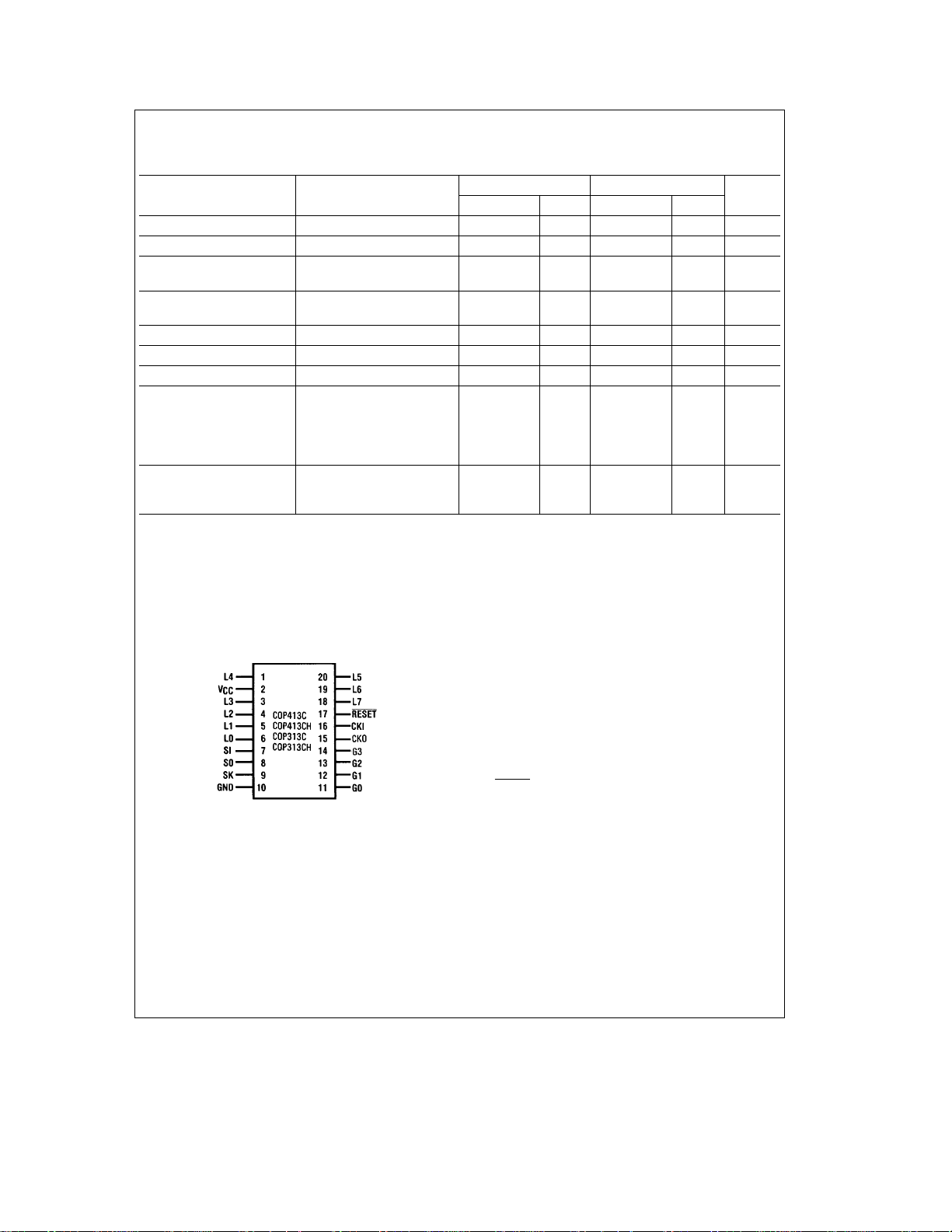
Pin Descriptions
Pin Description
L
7–L0
G
3–G0
SI Serial input (or counter input)
SO Serial output (or general purpose output)
SK Logic-controlled clock
CKI System oscillator input
CKO Crystal oscillator output, or NC
RESET
V
CC
GND System Ground
FIGURE 2
5
8-bit bidirectional I/O port with TRI-STATE
4-bit bidirectional I/O port
(or general purpose output)
System reset input
System power supply
Page 6

Timing Waveform
FIGURE 3. Input/Output Timing Diagrams (Divide-by-8 Mode)
Development Support
The MOLE (Microcontroller On Line Emulator) is a low cost
development system and real time emulator for COPS’
products. They also include TMP, 8050 and the new 16 bit
HPC microcontroller family. The MOLE provides effective
support for the development of both software and hardware
in the user’s application.
The purpose of the MOLE is to provide a tool to write and
assemble code, emulate code for the target microcontroller
and assist in debugging of the system.
The MOLE can be connected to various hosts, IBM PC,
STARPLEX
port. This link facilitates the up loading/down loading of
code, supports host assembly and mass storage.
The MOLE consists of three parts; brain, personality and
optional host software.
The brain board is the computing engine of the system. It is
a self-contained computer with its own firmware which provides for all system operation, emulation control, communication, from programming and diagnostic operation. It has
three serial ports which can be connected to a terminal,
host system, printer, modem or to other MOLE’s in a multiMOLE environment.
TM
, Kaypro, Apple and Intel systems, via RS-232
TL/DD/8537– 3
The personality board contains the necessary hardware and
firmware needed to emulate the target microcontroller. The
emulation cable which replaces the target controller attaches to this board. The software contains a cross assembler
and a communications program for up loading and down
loading code from the MOLE.
MOLE Ordering Information
P/N Description
MOLE-BRAIN MOLE Computer Board
MOLE-COPS-PB1 COPS Personality Board
MOLE-XXX-YYY Optional Software
Where XXX
e
COPS
e
YYY
Host System, IBM, Apple,
KAY (Kaypro), CP/M
6
Page 7

Functional Description
To ease reading of this description, only COP413C is refer-
enced; however, all such references apply equally to
COP413CH, COP313C, and COP313CH.
A block diagram of the COP413C is given in
paths are illustrated in simplified form to depict how the vari-
ous logic elements communicate with each other in imple-
menting the instruction set of the device. Positive logic is
used. When a bit is set, it is a logic ‘‘1’’; when a bit is reset, it
is a logic ‘‘0’’.
PROGRAM MEMORY
Program memory consists of a 512-byte ROM. As can be
seen by an examination of the COP413C instruction set,
these words may be program instructions, program data, or
ROM addressing data. Because of the special characteris-
tics associated with the JP, JSRP, JID, and LQID instruc-
tions, ROM must often be thought of as being organized into
8 pages of 64 words (bytes) each.
ROM ADDRESSING
ROM addressing is accomplished by a 9-bit PC register. Its
binary value selects one of the 512 8-bit words contained in
ROM. A new address is loaded into the PC register during
each instruction cycle. Unless the instruction is a transfer of
control instruction, the PC register is loaded with the next
sequential 9-bit binary count value. Two levels of subroutine
nesting are implemented by two 9-bit subroutine save regis-
ters, SA and SB.
ROM instruction words are fetched, decoded, and executed
by the instruction decode, control and skip logic circuitry.
DATA MEMORY
Data Memory consists of a 128-bit RAM, organized as four
data registers of 8
c
4-bit digits. RAM addressing is implemented by a 6-bit B register whose upper two bits (Br) selects one of four data registers and lower three bits of the 4bit Bd select one of eight 4-bit digits in the selected data
register. While the 4-bit contents of the selected RAM digit
(M) are usually loaded into or from, or exchanged with, the A
register (accumulator), they may also be loaded into the Q
latches or loaded from the L ports. RAM addressing may
also be performed directly by the XAD 3, 15 instruction.
The most significant bit of Bd is not used to select a RAM
digit. Hence, each physical digit of RAM may be selected by
two different values of Bd as shown in
condition for XIS and XDS instructions will be true if Bd
changes between 0 to 15, but
not
Table III).
Figure 1.
Figure 4.
Data
The skip
between 7 and 8 (see
INTERNAL LOGIC
The internal logic of the COP413C is designed to ensure
fully static operation of the device.
The 4-bit A register (accumulator) is the source and destination register for most I/O, arithmetic, logic and data memory
access operations. It can also be used to load the Bd portion of the B register, to load four bits of the 8-bit Q latch
data and to perform data exchanges with the SIO register.
The 4-bit adder performs the arithmetic and logic functions
of the COP413C, storing its results in A. It also outputs the
carry information to a 1-bit carry register, most often employed to indicate arithmetic overflow. The C register, in
conjunction with the XAS instruction and the EN register,
also serves to control the SK output. C can be outputted
directly to SK or can enable SK to be a sync clock each
instruction cycle time. (See XAS instruction and EN register
description below.)
The G register contents are outputs to four general purpose
bidirectional I/O ports.
The Q register is an internal, latched, 8-bit register, used to
hold data loaded from RAM and A, as well as 8-bit data from
ROM. Its contents are output to the L I/O ports when the L
drivers are enabled under program control. (See LEI instruction.)
The eight L drivers, when enabled, output the contents of
latched Q data to the L I/O ports. Also, the contents of L
may be read directly into A and RAM.
* Can be directly addressed by
LBI instruction (See Table 3)
TL/DD/8537– 4
FIGURE 4. RAM Digit Address to Physical
RAM Digit Mapping
7
Page 8

Functional Description (Continued)
The SIO register functions as a 4-bit serial-in/serial-out shift
register or as a binary counter, depending upon the contents of the EN register. (See EN register description below.) Its contents can be exchanged with A, allowing
it to input or output a continuous serial data stream. With
SIO functioning as a serial-in/serial-out shift register and SK
as a sync clock, the COP413C is MICROWIRE compatible.
The XAS instruction copies C into the SKL latch. In the
counter mode, SK is the output of SKL; in the shift register
mode, SK is a sync clock, inhibited when SKL is a logic ‘‘0’’.
The EN register is an internal 4-bit register loaded under
program control by the LEI instruction. The state of each bit
of this register selects or deselects the particular feature
associated with each bit of the EN register (EN3– EN0).
1. The least significant bit of the enable register, EN0, selects the SIO register as either a 4-bit shift register or as a
4-bit binary counter. With EN0 set, SIO is an asynchronous binary counter,
each low-going pulse (‘‘1’’ to ‘‘0’’) occurring on the SI
input. Each pulse must be at least two instruction cycles
wide. SK outputs the value of SKL. The SO output is
equal to the value of EN3. With EN0 reset, SIO is a serial
shift register, shifting left each instruction cycle time. The
data present at SI is shifted into the least significant bit of
SIO. SO can be enabled to output the most significant bit
of SIO each instruction cycle time. (See 4, below.) The
SK output becomes a logic-controlled clock.
2. EN 1 is not used, it has no effect on the COP413C.
3. With EN2 set, the L drivers are enabled to output the data
in Q to the L I/O ports. Resetting EN2 disables the L
drivers, placing the L I/O ports in a high impedance input
state.
4. EN3, in conjunction with EN0, affects the SO output. With
EN0 set (binary counter option selected), SO will output
the value loaded into EN3. With EN0 reset (serial shift
decrementing
its value by one upon
register option selected), setting EN3 enables SO as the
output of the SIO shift register, outputting serial shifted
data each instruction time. Resetting EN3 with the serial
shift register option selected, disables SO as the shift
register output; data continues to be shifted through SIO
and can be exchanged with A via an XAS instruction but
SO remains reset to ‘‘0’’.
INITIALIZATION
The external RC network shown in
nected to the RESET
pin. The RESET pin is configured as a
Figure 5
must be con-
Schmitt trigger input. If not used, it should be connected to
V
. Initialization will occur whenever a logic ‘‘0’’ is applied
CC
to the RESET
input, providing it stays low for at least three
instruction cycle times.
Upon initialization, the PC register is cleared to 0 (ROM address 0) and the A, B, C, EN, and G registers are cleared.
The SK output is enabled as a SYNC output, providing a
pulse each instruction cycle time. Data memory (RAM) is
not cleared upon initialization. The first instruction at address 0 must be a CLRA (clear A register).
RCl5cPower Supply Rise Time
l
100cCKI Period
and RC
TL/DD/8537– 5
FIGURE 5. Power-Up Clear Circuit
TABLE I. Enable Register ModesÐBits EN0 and EN3
EN0 EN3 SIO SI SO SK
0 0 Shift Register Input to Shift 0 If SKLe1, SKeclock
0 1 Shift Register Input to Shift Serial If SKL
Register If SKL
Register out If SKL
1 0 Binary Counter Input to Counter 0 SK
1 1 Binary Counter Input to Counter 1 SK
e
e
e
e
SKL
e
SKL
0, SKe0
1, SKeclock
0, SKe0
8
Page 9

Functional Description (Continued)
HALT MODE
The COP413C is a
stop the system oscillator at any time to halt the chip. The
chip may be halted by the HALT instruction. Once in the
HALT mode, the internal circuitry does not receive any clock
signal, and is therefore frozen in the exact state it was in
when halted. All information is retained until continuing. The
HALT mode is the minimum power dissipation state.
The HALT mode may be entered into by program control
(HALT instruction) which forces CKO to a logic ‘‘1’’ state.
The circuit can be awakened only by the RESET
POWER DISSIPATION
The lowest power drain is when the clock is stopped. As the
frequency increases so does current. Current is also lower
at lower operating voltages. Therefore, to minimize power
consumption, the user should run at the lowest speed and
voltage that his application will allow. The user should take
care that all pins swing to full supply levels to ensure that
outputs are not loaded down and that inputs are not at
some intermediate level which may draw current. Any input
with a slow rise or fall time will draw additional current. A
crystal- or resonator-generated clock will draw more than a
square-wave input. An RC oscillator will draw even more
current since the input is a slow rising signal.
If using an external squarewave oscillator, the following
equation can be used to calculate the COP413C current
drain.
eIqa
Ic
where Ic
For example, at 5V VCCand 400 kHz (divide by 8),
Ice30a(5c20c0.4)a(5c1280c0.4/8)
Ice30a40a320e390 mA
fully static
circuit; therefore, the user may
function.
(Vc20cFi)a(Vc1280cFl/Dv)
e
chip current drain in microamps
Iqequiescent leakage current (from curve)
FleCKI frequency in megahertz
Vechip VCCin volts
e
divide by option selected
Dv
OSCILLATOR OPTIONS
There are two options available that define the use of CKI
and CKO.
a. Cyrstal-Controlled Oscillator. CKI and CKO are connect-
ed to an external crystal. The instruction cycle time
equals the crystal frequency divided by 8.
b. RC-Controlled Oscillator. CKI is configured as a single
pin RC-controlled Schmitt trigger oscillator. The instruction cycle equals the oscillation frequency divided by 4.
CKO is NC.
The RC oscillator is not recommended in systems that require accurate timing or low current. The RC oscillator
draws more current than an external oscillator (typically an
additional 100 mA at 5V). However, when the part halts, it
stops with CKI high and the halt current is at the minimum.
TL/DD/8537– 6
FIGURE 6. COP413C Oscillator
Crystal or Resonator
RC-Controlled
Oscillator
Crystal Component Value Cycle
Value R1 R2 C1 pF C2 pF R C Time V
32 kHz 220k 20M 30 5– 36 15k 82 pF 4 – 9 ms
455 kHz 5k 10M 80 40 30k 82 pF 8– 16 ms
t
t
CC
4.5V COP413CH Only
4.5V COP413CH Only
2.000 MHz 2k 1M 30 6 –36 47k 100 pF 16–32 m s 3.0 to 4.5V COP413C Only
56k 100 pF 16–32 m s
Note: 15k
sRs
150k,
t
4.5V
50 pFsCs150 pF
9
Page 10

Functional Description (Continued)
I/O CONFIGURATIONS
COP413C outputs have the following configurations, illustrated in
Figure 7
:
a. Standard SO, SK Output. A CMOS push-pull buffer with
an N-channel device to ground in conjunction with a
P-channel device to V
LSTTL.
b. Low Current G Output. This is the same configuration as
(a) above except that the sourcing current is much less.
c. Standard TRI-STATE L Output. L output is a CMOS out-
put buffer similar to (a) which may be disabled by program control.
, compatible with CMOS and
CC
a. Standard Push-Pull Output b. Low Current Push-Pull Output
The SI and RESET
inputs are Hi-Z inputs (
Figure 7d
).
When using the G I/O port as an input, set the output register to a logic ‘‘1’’ level. The P-channel device will act as a
pull-up load. When using the L I/O port as an input, disable
the L drivers with the LEI instruction. The drivers are then in
TRI-STATE mode and can be driven externally.
All output drivers use one or more of three common devices
numbered 1 to 3. Minimum and maximum current (I
V
) curves are given in
OUT
to allow the designer to effectively use these I/O configura-
Figure 8
for each of these devices
OUT
and
tions.
c. Standard TRI-STATE
SO, SK, L Port, G Port
Minimum Sink Current
COP413C/COP413CH
Low Current G Port
Maximum Source Current
‘‘L’’ Output
FIGURE 7. I/O Configurations
SO, SK, L Port Standard
Minimum Source Current
COP313C/COP313CH
Low Current G Port
Maximum Source Current Maximum Quiescent Current
d. Hi-Z Input
TL/DD/8537– 7
G Port Low Current
Minimum Source Current
FIGURE 8
10
TL/DD/8537– 8
Page 11

COP413C Instruction Set
Table II is a symbol table providing internal architecture, instruction operand and operational symbols used in the instruction set table.
TABLE II. COP413C Instruction Set Table Symbols
Symbol Definition
INTERNAL ARCHITECTURE SYMBOLS
A 4-bit Accumulator
B 6-bit RAM Address Register
Br Upper 2 bits of B (register address)
Bd Lower 4 bits of B (digit address)
C 1-bit Carry Register
EN 4-bit Enable Register
G 4-bit Register to latch data for G I/O Port
L 8-bit TRI-STATE I/O Port
M 4-bit contents of RAM Memory pointed to by B
Register
PC 9-bit ROM Address Register (program counter)
Q 8-bit Register to latch data for L I/O Port
SA 9-bit Subroutine Save Register A
SB 9-bit Subroutine Save Register B
SIO 4-bit Shift Register and Counter
SK Logic-Controlled Clock Output
Table III provides the mnemonic, operand, machine code,
data flow, skip conditions and description associated with
each instruction in the COP413C instruction set.
Symbol Definition
INSTRUCTION OPERAND SYMBOLS
d 4-bit Operand Field, 0 –15 binary (RAM Digit Select)
r 2-bit Operand Field, 0 – 3 binary (RAM Register
Select)
a 9-bit Operand Field, 0 – 511 binary (ROM Address)
y 4-bit Operand Field, 0 –15 binary (Immediate Data)
RAM(s) Contents of RAM location addressed by s
ROM(t) Contents of ROM location addressed by t
OPERATIONAL SYMBOLS
a
Plus
b
Minus
x
Replaces
Ý
Is exchanged with
e
Is equal to
A
The one’s complement of A
Z
Exclusive-OR
: Range of values
Mnemonic Operand
ARITHMETIC INSTRUCTIONS
ASC 30
ADD 31
AISC y 5
CLRA 00
COMP 40
NOP 44
RC 32
SC 22
XOR 02
Hex
Code
b
TABLE III. COP413C Instruction Set
Machine
Language Code Data Flow Skip Conditions Description
(Binary)
0011À0000ÀAaCaRAM(B)xA Carry Add with Carry, Skip on
À
0011À0001
À
0101Ày
À
0000À0000À0xA None Clear A
À
0100À0000
À
0100À0100
À
0011À0010
À
0010À0010À‘‘1’’xC None Set C
À
0000À0010
À
Carry
x
C Carry
AaRAM(B)xA None Add RAM to A
À
AayxA Carry Add immediate, Skip on
À
AxA None One’s complement of A to A
À
None None No Operation
À
‘‘0’’xC None Reset C
À
AZRAM(B)xA None Exclusive-OR RAM with A
À
11
Carry (y
i
0)
Page 12

COP413C Instruction Set (Continued)
TABLE III. COP413C Instruction Set (Continued)
Mnemonic Operand
TRANSFER OF CONTROL INSTRUCTIONS
JID FF
JMP a 6
JP a –
JSRP a –
JSR a 6
RET 48
RETSK 49
HALT 33
MEMORY REFERENCE INSTRUCTIONS
CAMQ 33
CQMA 33
LD r
LQID BF
RMB 0 4C
SMB 0 4D
STII y 7
Xr
XAD 3,15 23
Hex
Code
–
–
–
38
3C
2C
b
145
242
343
147
246
34B
b
BF
Machine
Language Code Data Flow Skip Conditions Description
(Binary)
1111À1111ÀROM (PC8, A,M)
À
b
0110À000Àa
À
À
À1À
(pages 2, 3 only) (Note 1)
À11À
(all other pages)
À10À
b
0110À100Àa
À
À
0100À1000
À
0100À10011
À
0011À0011
À
0011À1000
À
0011À0011ÀAxQ
À
0011À1100
À
0011À0011ÀQ
À
0010À1100
À
5
À00ÀrÀ
1011À1111ÀROM(PC8,A,M)xQ None Load Q Indirect
À
0100À1100
À
0100À0101
À
0100À0010À0xRAM(B)
À
0100À0011À0xRAM(B)
À
0100À1101À1xRAM(B)
À
0100À0111
À
0100À0110À1xRAM(B)
À
0100À1011À1xRAM(B)
À
b
0111Ày
À
6
00ÀrÀ0110ÀRAM(B)
À
0010À0011
À
1011À1111
À
8
À
a
7:0
À
a
6:0
À
or
a
5:0
À
a
5:0
À
8
À
a
7:0
À
À
À
À
À
À
À
0101ÀRAM(B)xA None Load RAM into A
À
À
À
À
À
À
PC
7:0
axPC None Jump
axPC
axPC
PCa1xSAxSB None Jump to Subroutine Page
x
010
axPC
PCa1xSAxSB None Jump to Subroutine
axPC
SBxSAxPC None Return from Subroutine
SBxSAxPC Always Skip on Return Return from Subroutine
RAM(B)xQ
x
7:4
Q
x
3:0
Z
rxBr Exclusive-OR Br with r
Br
x
SA
0xRAM(B)
0xRAM(B)
1xRAM(B)
yxRAM(B) None Store Memory Immediate
a
1xBd and Increment Bd
Bd
BrZrxBr Exclusive-OR Br with r
RAM(3,15)
x
6:0
5:0
PC
8:6
5:0
7:4
3:0
RAM(B) None Copy Q to RAM, A
A
SB
0
1
2
3
0
1
2
3
Ý
A None Exchange RAM with A,
Ý
None Jump Indirect (Note 2)
None Jump within Page
(Note 2)
then Skip
None Halt processor
None Copy A, RAM to Q
None Reset RAM Bit
None Set RAM Bit
A None Exchange A with RAM
(3,15)
12
Page 13

COP413C Instruction Set (Continued)
TABLE III. COP413C Instruction Set (Continued)
Mnemonic Operand
MEMORY REFERENCE INSTRUCTIONS (Continued)
XDS r
Hex
Code
b
Machine
Language Code Data Flow Skip Conditions Description
(Binary)
7
0111ÀRAM(B)
À00ÀrÀ
Ý
Bd–1
Z
Br
rxBr Exclusive-OR Br with r
A Bd decrements past 0 Exchange RAM with A
x
Bd and Decrement Bd
XIS r
REGISTER REFERENCE INSTRUCTIONS
CAB 50
CBA 4E
LBI r,d –
LEI y 33
TEST INSTRUCTIONS
SKC 20
SKE 21
SKGZ 33
SKGBZ 33
SKMBZ 0 01
INPUT/OUTPUT INSTRUCTIONS
ING 33
b
4
b
6
21
001
111
203
313
111
203
313
2A
À00ÀrÀ
0101À0000ÀAxBd None Copy A to Bd
À
0100À1110
À
À00ÀrÀ
e
(d
0011À0011ÀyxEN None Load EN Immediate
À
0010Ày
À
0010À0000
À
0010À0001
À
0011À0011
À
0010À0001
À
0011À0011
À
0000À0001
À
0001À0001
À
0000À0011
À
0010À0011
À
0000À0001
À
0001À0001
À
0000À0011
À
0001À0011
À
0011À0011ÀGxA None Input G Ports to A
À
0010À1010
À
0100ÀRAM(B)
À
(d-1)
À
0,9:15) r,d
À
À
À
À
À
À
À
À
À
À
À
À
À
À
À
Ý
a
Bd
Z
Br
rxBr Exclusive-OR Br with r
BdxA None Copy Bd to A
r,dxB Skip until not a LBI Load B Immediate with
1st byte Skip if G Bit is Zero
2nd byte
* G
A Bd increments past 15 Exchange RAM with A
1xBd and Increment Bd
Ce‘‘1’’ Skip if C is True
AeRAM(B) Skip if A Equals RAM
e
G
0 Skip if G is Zero
3:0
e
G
0
0
e
0
G
1
e
G
0
2
e
0
3
RAM(B)
RAM(B)
RAM(B)
RAM(B)
e
0 Skip if RAM Bit is Zero
0
e
0
1
e
0
2
e
0
3
(all 4 bits)
INL 33
OMG 33
XAS 4F
Note 1: The JP instruction allows a jump, while in subroutine pages 2 or 3, to any ROM location within the two-page boundary of pages 2 or 3. The JP instruction,
otherwise, permits a jump to a ROM location within the current 64-word page. JP may not jump to the last word of a page.
Note 2: A JSRP transfers program control to subroutine page 2 (0010 is loaded into the upper 4 bits of P). A JSRP may not be used when in pages 2 or 3. JSRP
may not jump to the last word in page 2.
2E
3A
0011À0011ÀL
À
0010À1110
À
0011À0011
À
0011À1010
À
0100À1111ÀA
À
À
À
À
x
RAM(B) None Input L Ports to RAM, A
7:4
L
x
A
3:0
RAM(B)xG None Output RAM to G Ports
Ý
SIO, CxSKL None Exchange A with SIO
13
Page 14

Description of Selected Instructions
The following information is provided to assist the user in
understanding the operation of several unique instructions
and to provide notes useful to programmers in writing
COP413C programs.
XAS INSTRUCTION
XAS (Exchange A with SIO) exchanges the 4-bit contents of
the accumulator with the 4-bit contents of the SIO register.
The contents of SIO will contain serial-in/serial-out shift register or binary counter data, depending on the value of the
EN register. An XAS instruction will also affect the SK output. (See Functional Description, EN Register.) If SIO is selected as a shift register, an XAS instruction must be performed once every four instruction cycle times to effect a
continuous data stream.
JID INSTRUCTION
JID (Jump Indirect) is an indirect addressing instruction,
transferring program control to a new ROM location pointed
to indirectly by A and M. It loads the lower eight bits of the
ROM address register PC with the contents of ROM addressed by the 9-bit word, PC
this instruction.
Note: JID uses two instruction cycles if executed, one if skipped.
LQID INSTRUCTION
LQID (Load Q Indirect) loads the 8-bit Q register with the
contents of ROM pointed to by the 9-bit word PC
LQID can be used for table look-up or code conversion such
as BCD to 7-segment. The LQID instruction ‘‘pushes’’ the
stack (PC
significant eight bits of the PC as follows: A
RAM(B)
pointed to by the new address is fetched and loaded into
the Q latches. Next, the stack is ‘‘popped’’ (SB
PC), restoring the saved value of the PC to continue sequential program execution. Since LQID pushes SA
SB, the previous contents of SB are lost.
Note: LQID uses two instruction cycles if executed, one if skipped.
x
a
1xSA
PC
, leaving PC8unchanged. The ROM data
3:0
,A,M.PC8is not affected by
8
x
SB) and replaces the least
x
xSAx
,A,M.
8
PC
x
7:4
INSTRUCTION SET NOTES
a. The first word of a COP413C program (ROM address 0)
must be a CLRA (Clear A) instruction.
b. Although skipped instructions are not executed, one in-
struction cycle time is devoted to skipping each byte of
the skipped instruction. Thus all program paths take the
same number of cycle times whether instructions are
skipped or executed (except JID and LQID).
c. The ROM is organized into eight pages of 64 words each.
The program counter is a 9-bit binary counter, and will
count through page boundaries. If a JP, JSRP, JID, or
LQID instruction is located in the last word of a page, the
instruction operates as if it were in the next page. For
example: A JP located in the last word of a page will jump
to a location in the next page. Also, a LQID or JID located
in the last word in page 3 or 7 will access data in the next
group of four pages.
COPS Programming Manual
For detailed information on writing. COPS programs, the
COPS Programming Manual 424410284-001 provides an indepth discussion of the COPS architecture, instruction set
and general techniques of COPS programming. This manual
is written with the programmer in mind.
OPTION LISTÐOSCILLATOR SELECTION
The oscillator option selected must be sent in with the
EPROM of ROM Code for masking into the COP413C. Select the appropriate option, make a photocopy of the table
and send it with the EPROM.
,
COP413C/COP313C
Option 1: Oscillator selection
e
0 Ceramic Resonator input frequency divided by 8.
CKO is oscillator output.
e
1 Single pin RC controlled oscillator divided by 4. CKO
is no connection.
Note: The following option information is to be sent to National along with the EPROM.
Option 1: Value
e
is Oscillator Selected.
ÐÐ
14
Page 15

Physical Dimensions inches (millimeters)
20-Lead Hermetic Dual-In-Line Package (D)
Order Number COP313C–XXX/D, COP313CH –XXX/D,
COP413C–XXX/D, COP413CH –XXX/D
NS Package Number D20A
15
Page 16

Physical Dimensions inches (millimeters) (Continued) Lit.
20-Lead Molded Dual-In-Line Package (N)
Order Number COP313C–XXX/N, COP313CH –XXX/N,
COP413C–XXX/N or COP413CH –XXX/N
NS Package Number N20A
Ý
101975
LIFE SUPPORT POLICY
NATIONAL’S PRODUCTS ARE NOT AUTHORIZED FOR USE AS CRITICAL COMPONENTS IN LIFE SUPPORT
DEVICES OR SYSTEMS WITHOUT THE EXPRESS WRITTEN APPROVAL OF THE PRESIDENT OF NATIONAL
SEMICONDUCTOR CORPORATION. As used herein:
1. Life support devices or systems are devices or 2. A critical component is any component of a life
systems which, (a) are intended for surgical implant support device or system whose failure to perform can
into the body, or (b) support or sustain life, and whose be reasonably expected to cause the failure of the life
COP413C/COP413CH/COP313C/COP313CH Single-Chip CMOS Microcontrollers
failure to perform, when properly used in accordance support device or system, or to affect its safety or
with instructions for use provided in the labeling, can effectiveness.
be reasonably expected to result in a significant injury
to the user.
National Semiconductor National Semiconductor National Semiconductor National Semiconductor
Corporation Europe Hong Kong Ltd. Japan Ltd.
1111 West Bardin Road Fax: (
Arlington, TX 76017 Email: cnjwge@tevm2.nsc.com Ocean Centre, 5 Canton Rd. Fax: 81-043-299-2408
Tel: 1(800) 272-9959 Deutsch Tel: (
Fax: 1(800) 737-7018 English Tel: (
National does not assume any responsibility for use of any circuitry described, no circuit patent licenses are implied and National reserves the right at any time without notice to change said circuitry and specifications.
Fran3ais Tel: (
Italiano Tel: (
a
49) 0-180-530 85 86 13th Floor, Straight Block, Tel: 81-043-299-2309
a
49) 0-180-530 85 85 Tsimshatsui, Kowloon
a
49) 0-180-532 78 32 Hong Kong
a
49) 0-180-532 93 58 Tel: (852) 2737-1600
a
49) 0-180-534 16 80 Fax: (852) 2736-9960
 Loading...