

Page 1
查询COP404C供应商
COP404C ROMless CMOS Microcontrollers
COP404C ROMless CMOS Microcontrollers
April 1992
General Description
The COP404C ROMless Microcontroller is a member of the
TM
COPS
family, fabricated using double-poly, silicon gate
CMOS (microCMOS) technology. The COP404C contains
CPU, RAM, I/O and is identical to a COP444C device except the ROM has been removed and pins have been added to output the ROM address and to input the ROM data.
The COP404C can be configured, by means of external
pins, to function as a COP444C, a COP424C, or a
COP410C. Pins have been added to allow the user to select
the various functional options that are available on the family of mask-programmed CMOS parts. The COP404C is primarily intended for use in the development and debug of a
COP program for the COP444C/445C, COP424C/425C,
and COP410C/411C devices prior to masking the final part.
The COP404C is also appropriate in low volume applications or when the program might be changing.
MICROBUSTMand MICROWIRETMare trademarks of National Semiconductor Corporation.
TRI-STATE
is a registered trademark of National Semiconductor Corporation.
É
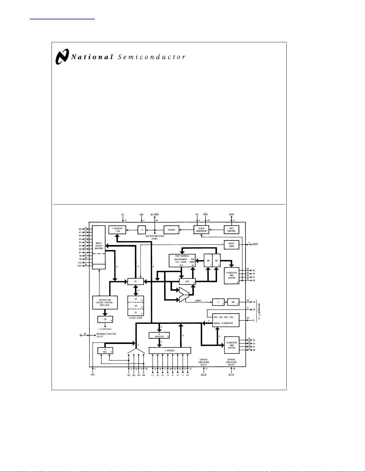
Block Diagram
Features
Y
Accurate emulation of the COP444C, COP424C and
COP410C
Y
Lowest Power Dissipation (50 mW typical)
Y
Fully static (can turn off the clock)
Y
Power saving IDLE state and HALT mode
Y
4 ms instruction time, plus software selectable clocks
Y
128c4 RAM, addresses 2kc8 ROM
Y
True vectored interrupt, plus restart
Y
Three-level subroutine stack
Y
Single supply operation (2.4V to 5.5V)
Y
Programmable read/write 8-bit timer/event counter
Y
Internal binary counter register with MICROWIRE
serial I/O capability
Y
General purpose and TRI-STATEÉoutputs
Y
LSTTL/CMOS compatible
Y
MICROBUSTMcompatible
Y
Software/hardware compatible with other members of
the COP400 family
TM
TL/DD/5530– 1
FIGURE 1. Block Diagram
C
1995 National Semiconductor Corporation RRD-B30M105/Printed in U. S. A.
TL/DD/5530
Page 2
Absolute Maximum Ratings
Supply Voltage 6V
Voltage at any pin
Total Allowable Source Current 25 mA
Total Allowable Sink Current 25 mA
b
0.3V to V
CC
a
0.3V
Operating temperature range 0§toa70§C
Storage temperature range
b
65§Ctoa150§C
Lead temperature (soldering, 10 sec.) 300§C
DC Electrical Characteristics 0
s
CsT
70§C unless otherwise specified
§
a
Parameter Conditions Min Max Units
Operating Voltage 2.4 5.5 V
Power Supply Ripple peak to peak 0.1 V
(Notes 4, 5)
Supply Current V
(Note 1) V
HALT Mode Current V
(Note 2) V
e
CC
e
CC
e
V
CC
(T
is instruction cycle time)
c
e
CC
e
CC
2.4V, t
5.0V, t
5.0V, t
5.0V, F
2.4V, F
e
64 ms 120 mA
c
e
16 ms 700 mA
c
e
4 ms 3000 mA
c
e
IN
e
IN
0 kHz, T
0 kHz, T
e
25§C20mA
A
e
25§C6mA
A
CC
V
Input Voltage Levels
RESET
, D0 (clock input)
CKI
Logic High 0.9 V
Logic Low 0.1 V
CC
All other inputs (Note 7)
Logic High 0.7 V
Logic Low 0.2 V
CC
CC
CC
V
V
V
V
Input Pull-up
current V
Hi-Z input leakage
CC
e
4.5V, V
e
0 30 330 mA
IN
b
1
a
1 mA
Input capacitance 7pF
(Note 4)
Output Voltage Levels Standard outputs
LSTTL Operation V
Logic High I
Logic Low I
CMOS Operation
Logic High I
Logic Low I
e
5.0Vg10%
CC
eb
100 mA 2.7 V
OH
e
400 mA 0.4 V
OL
eb
10 mAV
OH
e
10 mA 0.2 V
OL
b
0.2 V
CC
Output current levels
Sink (Note 6) V
Source (Standard option) V
Source (Low current option) V
e
4.5V, V
CC
e
V
2.4V, V
CC
e
4.5V, V
CC
e
V
2.4V, V
CC
e
4.5V, V
CC
e
V
2.4V, V
CC
e
V
OUT
CC
e
V
OUT
CC
e
0V 0.5 mA
OUT
e
0V 0.1 mA
OUT
e
0V 30 330 mA
OUT
e
0V 6 80 mA
OUT
1.2 mA
0.2 mA
Allowable Sink/Source current per pin 5 mA
(Note 6)
Allowable Loading on CKOH 100 pF
Current needed to over-ride HALT
(Note 3)
To continue V
To halt V
CC
CC
e
e
TRI-STATE leakage current
Note: Absolute maximum ratings indicate limits beyond which damage to the device may occur. DC and AC electrical specifications are not ensured when
operating the device at absolute maximum ratings.
4.5V, V
4.5V, V
e
2V
IN
CC
e
7V
IN
CC
b
2.5
.7 mA
1.6 mA
a
2.5 mA
2
Page 3
COP404C
s
AC Electrical Characteristics
0§CsT
Parameter Conditions Min Max Units
Instruction Cycle V
) 4.5VlV
Time (t
c
Operating CKI V
Frequency 4.5V
Duty Cycle (Note 4) f
Rise Time (Note 4) f
Fall Time (Note 4) 40 ns
Instruction Cycle Re30k, V
Time using D0 as a C
RC Oscillator DualClock Input (Note 4)
INPUTS: (See
t
SETUP
t
HOLD
OUTPUT
PROPAGATION DELAY V
IP7±IP0, A10 ±A8, SKIP
t
PD1,tPD0
AD/DATA
t
PD1,tPD0
ALL OTHER OUTPUTS
t
PD1
MICROBUS TIMING C
Read Operation (
Chip select stable before RDbt
Chip select hold time for RDbt
RD pulse widthbt
Data delay from RDbt
Fig. 3
)
,t
PD0
Fig. 4
)
CSR
RCS
RR
RD
CC
CC
e
1
e
1
e
G Inputs Tc/4a.7 ms
SI Input
IP Input 1.0 ms
All Others
V
CC
4.5V
OUT
V
CC
4.5VlV
V
CC
4.5V
V
CC
4.5V
e
L
RD to data floatingbtDF(Note 4) 250 ns
Write Operation (
Chip select stable before WRbt
Chip select hold time for WRbt
WR pulse widthbt
Data set-up time for WRbt
Data hold time for WRbt
INTR transition time from WRbt
Note 1: Supply current is measured after running for 2000 cycle times with a square-wave clock on CKI and all other pins pulled up to VCCwith 20k resistors. See
current drain equation on page 16.
Note 2: Test conditions: All inputs tied to V
Note 3: When forcing HALT, current is only needed for a short time (approx. 200 ns) to flip the HALT flip-flop.
Note 4: This parameter is only sampled and not 100% tested. Variation due to the device included.
Note 5: Voltage change must be less than 0.1 V
Note 6: SO output sink current must be limited to keep V
Note 7: MB
Fig. 5
)
CSW
WCS
WW
DW
WD
WI
; L lines in TRI-STATE mode and tied to Ground; all outputs tied to Ground.
CC
ina1msperiod.
CC
less than 0.2 VCCto prevent entering test mode.
, TIN, DUAL, SEL10, SEL20, input levels at VCCor VSS.
OL
70§C unless otherwise specified
A
t
4.5V 4 DC ms
t
2.4V 16 DC ms
CC
t
4.5V DC 1.0 MHz
t
l
V
2.4V DC 250 kHz
CC
4 MHz 40 60 %
4 MHz external clock 60 ns
e
5V
CC
82 pF 8 16 m s
t
V
4.5V
CC
* 1.7 m s
t
4.5V 0.25 ms
t
l
V
2.4V 1.0 m s
CC
e
t
4.5V 1.94 ms
t
4.5V 375 ns
l
l
4.5V 1.0 ms
l
50 pF, V
e
1.5V, C
CC
V
CC
V
CC
100 pF, R
L
t
2.4V 7.75 ms
t
2.4V 1.5 ms
t
2.4V 4.0 ms
e
5Vg5%
CC
e
5K
L
0.3 ms
65 ns
20 ns
400 ns
375 ns
65 ns
20 ns
400 ns
320 ns
100 ns
700 ns
3
Page 4
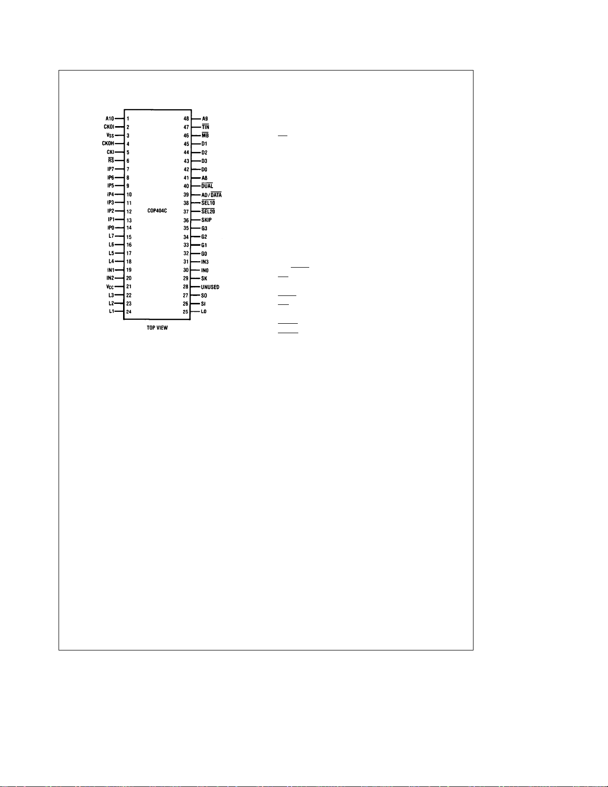
Connection Diagram
Dual-In-Line Package
Order Number COP404CN
See NS Package Number N48A
TL/DD/5530– 2
Pin Descriptions
Pin Description
V
CC
V
SS
CKI Clock input
RS
CKOI General purpose input
L0±L7 8 TRI-STATE I/O
G0±G3 4 general purpose I/O
D1±D3 3 general purpose outputs
D0 Either general purpose output
IN0±IN3 4 general purpose inputs
SO Serial data output
SI Serial data input
SK Serial data clock output
IP0±IP7 I/O for ROM address and data
A8, A9, A10 3 address outputs
SKIP Skip status output
AD/DATA
MB
CKOH Halt I/O pin
DUAL
TIN
SEL10
SEL20
UNUSED Ground
FIGURE 2
Most positive voltage
Ground
Reset input
or Dual-Clock RC input
Clock output
MICROBUS select input
Dual-Clock select input
Timer input select pin (should be
connected to GND)
COP410C emulation select input
COP424C emulation select input
Figure 1
The internal architecture is shown in
are illustrated in simplified form to depict how the various
logic elements communicate with each other in implementing the instruction set of the device. Positive logic is used.
When a bit is set, it is a logic ‘‘1’’, when a bit is reset, it is a
logic ‘‘0’’.
PROGRAM MEMORY
Program Memory consists of a 2048-byte external memory
(typically PROM). Words of this memory may be program
instructions, constants or ROM addressing data.
ROM addressing is accomplished by a 11-bit PC register
which selects one of the 8-bit words contained in ROM. A
new address is loaded into the PC register during each instruction cycle. Unless the instruction is a transfer of control
instruction, the PC register is loaded with the next sequential 11-bit binary count value.
Three levels of subroutine nesting are implemented by a
three level deep stack. Each subroutine call or interrupt
. Data paths
pushes the next PC address into the stack. Each return
pops the stack back into the PC register.
DATA MEMORY
Data memory consists of a 512-bit RAM, organized as 8
data registers of 16
mented by a 7-bit B register whose upper 3 bits (B
of 8 data registers and lower 4 bits (B
digits in the selected data register. While the 4-bit contents
of the selected RAM digit (M) are usually loaded into or
from, or exchanged with, the A register (accumulator), it
may also be loaded into or from the Q latches or T counter
or loaded from the L ports. RAM addressing may also be
performed directly by the LDD and XAD instructions based
upon the immediate operand field of these instructions. The
B
register also serves as a source register for 4-bit data
d
sent directly to the D outputs.
4
c
4-bit digits. RAM addressing is imple-
) select 1 of 16 4-bit
d
) select 1
r
Page 5
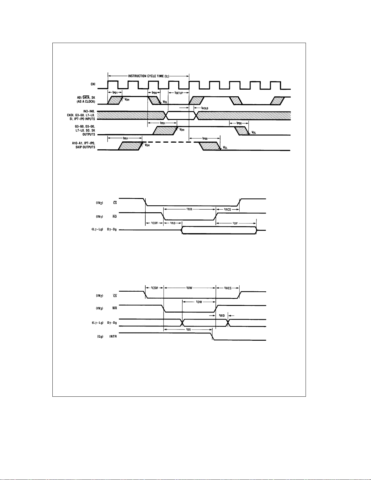
Timing Diagrams
FIGURE 3. Input/Output Timing
FIGURE 4. MICROBUS Read Operation Timing
TL/DD/5530– 3
TL/DD/5530– 4
FIGURE 5. MICROBUS Write Operation Timing
5
TL/DD/5530– 5
Page 6

Functional Description
INTERNAL LOGIC
The processor contains its own 4-bit A register (accumulator) which is the source and destination register for most
I/O, arithmetic, logic, and data memory access operations.
It can also be used to load the B
register, to load and input 4 bits of the 8-bit Q latch or T
counter, L I/O ports data, to input 4-bit G, or IN ports, and to
perform data exchanges with the SIO register.
A 4-bit adder performs the arithmetic and logic functions,
storing the results in A. It also outputs a carry bit to the 1-bit
C register, most often employed to indicate arithmetic overflow. The C register in conjunction with the XAS instruction
and the EN register, also serves to control the SK output.
The 8-bit T counter is a binary up counter which can be
loaded to and from M and A using CAMT and CTMA instructions. This counter is operated as a time-base counter.
When the T counter overflows, an overflow flag will be set
(see SKT and IT instructions below). The T counter is
cleared on reset. A functional block diagram of the timer/
counter is illustrated in
Figure 10a
Four general-purpose inputs, IN3 –IN0, are provided. IN1,
IN2 and IN3 may be selected (by pulling MB
Read Strobe, Chip Select, and Write Strobe inputs, respectively, for use in MICROBUS application.
The D register provides 4 general-purpose outputs and is
used as the destination register for the 4-bit contents of B
In the dual clock mode, D0 latch controls the clock selection
(see dual oscillator below).
The G register contents are outputs to a 4-bit general-purpose bidirectional I/O port. G0 may be selected as an output for MICROBUS applications.
The Q register is an internal, latched, 8-bit register, used to
hold data loaded to or from M and A, as well as 8-bit data
from ROM. Its contents are outputted to the L I/O ports
when the L drivers are enabled under program control. With
the MICROBUS option selected, Q can also be loaded with
the 8-bit contents of the L I/O ports upon the occurrence of
a write strobe from the host CPU.
The 8 L drivers, when enabled, output the contents of
latched Q data to the L I/O port. Also, the contents of L may
be read directly into A and M. As explained above, the MICROBUS option allows L I/O port data to be latched into
the Q register.
The SIO register functions as a 4-bit serial-in/serial-out shift
register for MICROWIRE
as a binary counter (depending on the contents of the EN
register). Its contents can be exchanged with A.
The XAS instruction copies C into the SKL latch. In the
counter mode, SK is the output SKL; in the shift register
mode, SK outputs SKL ANDed with the clock.
and Bdportions of the B
r
.
pin low) as
TM
I/O and COPS peripherals, or
EN is an internal 4-bit register loaded by the LEI instruction.
The state of each bit of this register selects or deselects the
particular feature associated with each bit of the EN register:
0. The least significant bit of the enable register, EN0, selects the SIO register as either a 4-bit shift register or a 4bit binary counter. With EN0 set, SIO is an asynchronous
binary counter, decrementing its value by one upon each
low-going pulse (‘‘1’’ to ‘‘0’’) occurring on the SI input.
Each pulse must be at least two instruction cycles wide.
SK outputs the value of SKL. The SO output equals the
value of EN3. With EN0 reset, SIO is a serial shift register
left shifting 1 bit each instruction cycle time. The data
present at SI goes into the least significant bit of SIO. SO
can be enabled to output the most significant bit of SIO
each cycle time. The SK outputs SKL ANDed with the
instruction cycle clock.
1. With EN1 set, interrupt is enabled. Immediately following
an interrupt, EN1 is reset to disable further interrupts.
2. With EN2 set, the L drivers are enabled to output the data
in Q to the L I/O port. Resetting EN2 disables the L drivers, placing the L I/O port in a high-impedance input
state.
3. EN3, in conjunction with EN0, affects the SO output. With
EN0 set (binary counter option selected) SO will output
.
d
the value loaded into EN3. With EN0 reset (serial shift
register option selected), setting EN3 enables SO as the
output of the SIO shift register, outputting serial shifted
data each instruction time. Resetting EN3 with the serial
shift register option selected disables SO as the shift register output; data continues to be shifted through SIO and
can be exchanged with A via an XAS instruction but SO
remains set to ‘‘0’’.
INTERRUPT
The following features are associated with interrupt procedure and protocol and must be considered by the programmer when utilizing interrupts.
a. The interrupt, once recognized as explained below,
pushes the next sequential program counter address
a
(PC
1) onto the stack. Any previous contents at the bottom of the stack are lost. The program counter is set to
hex address 0FF (the last word of page 3) and EN1 is
reset.
b. An interrupt will be recognized only on the following con-
ditions:
1. EN1 has been set.
2. A low-going pulse (‘‘1’’ to ‘‘0’’) at least two instruction
cycles wide has occurred on the IN1 input.
3. A currently executing instruction has been completed.
TABLE I. ENABLE REGISTER MODES Ð BITS EN0 AND EN3
EN0 EN3 SIO SI SO SK
0 0 Shift Register Input to Shift 0 If SKLe1, SKeclock
e
0 1 Shift Register Input to Shift Serial If SKL
Register If SKL
Register out If SKL
1 0 Binary Counter Input to Counter 0 SK
1 1 Binary Counter Input to Counter 1 SK
0, SKe0
e
1, SKeclock
e
0, SKe0
e
SKL
e
SKL
6
Page 7

Functional Description (Continued)
4. All successive transfer of control instructions and successive LBIs have been completed (e.g. if the main
program is executing a JP instruction which transfers
program control to another JP instruction, the interrupt
will not be acknowledged until the second JP instruction has been executed).
c. Upon acknowledgement of an interrupt, the skip logic
status is saved and later restored upon popping of the
stack. For example, if an interrupt occurs during the execution of an ASC (Add with Carry, Skip on Carry) instruction which results in carry, the skip logic status is saved
and program control is transferred to the interrupt servicing routine at hex address 0FF. At the end of the interrupt
routine, a RET instruction is executed to pop the stack
and return program control to the instruction following the
original ASC. At this time, the skip logic is enabled and
skips this instruction because of the previous ASC carry.
Subroutines should not be nested within the interrupt
service routine, since their popping of the stack will enable any previously saved main program skips, interfering
with the orderly execution of the interrupt routine.
d. The instruction at hex address 0FF must be a NOP.
e. An LEI instruction may be put immediately before the
RET instruction to re-enable interrupts.
MICROBUS INTERFACE
With MB
pin tied to Ground, the COP404C can be used as a
peripheral microprocessor device, inputting and outputting
data from and to a host microprocessor (mP). IN1, IN2 and
IN3 general purpose inputs become MICROBUS compatible
read-strobe, chip-select, and write-strobe lines, respectively.
IN1 becomes RD
latch data to be enabled to the L ports for input to the m P.
IN2 becomes CS
COP404C and the mP peripheral device by enabling the operation of the RD
of one of several peripheral components. IN3 becomes WR
Ð a logic ‘‘0’’ on this line will write bus data from the L ports
to the Q latches for input to the COP404C. G0 becomes
INTR a ‘‘ready’’ output, reset by a write pulse from the mP
on the WR
essary for asynchronous data transfer between the host
CPU and the COP404C.
This option has been designed for compatibility with National’s MICROBUS - a standard interconnect system for 8-bit
parallel data transfer between MOS/LSI CPUs and interfacing devices. (See MICROBUS National Publication). The
Ð a logic ‘‘0’’ on this input will cause Q
Ð a logic ‘‘0’’ on this line selects the
and WR lines and allows for the selection
line, providing the ‘‘handshaking’’ capability nec-
functioning and timing relationships between the signal lines
affected by this option are as specified for the MICROBUS
interface, and are given in the AC electrical characteristics
and shown in the timing diagrams (
nection of the COP404C to the MICROBUS is shown in
ure 6
.
INITIALIZATION
The external RC network shown in
nected to the RESET
ize the device upon power-up. The RESET
as a Schmitt trigger input. If not used, it should be connected to V
applied to the RESET
least three instruction cycle times.
Upon initialization, the PC register is cleared to 0 (ROM address 0) and the A, B, C, D, EN, IL, T and G registers are
cleared. The SKL latch is set, thus enabling SK as a clock
output. Data Memory (RAM) is not cleared upon initialization. The first instruction at address 0 must be a CLRA
(clear A register).
TIMER
The timer is operated as a time-base counter. The instruction cycle frequency generated from CKI passes through a
2-bit divide-by-4 prescaler. The output of this prescaler increments the 8-bit T counter thus providing a 10-bit timer.
The prescaler is cleared during execution of a CAMT instruction and on reset. For example, using a 1MHz crystal,
the instruction cycle frequency of 250 kHz (divide by 4) increments the 10-bit timer every 4 mS. By presetting the
counter and detecting overflow, accurate timeouts between
16 mS (4 counts) and 4.096 mS (1024 counts) are possible.
Longer timeouts can be achieved by accumulating, under
software control, multiple overflows.
HALT MODE
The COP404C is a FULLY STATIC circuit; therefore, the
user may stop the system oscillator at any time to halt the
chip. The chip may also be halted by two other ways (see
Figure 8
. Initialization will occur whenever a logic ‘‘0’’ is
CC
):
Ð Software HALT: by using the HALT instruction.
Ð Hardware HALT: by using the HALT I/O port CKOH. It
is an I/O flip-flop which is an indicator of the HALT
status. An external signal can over-ride this pin to start
and stop the chip. By forcing CKOH high the
pin for the internal reset logic to initial-
input, providing it stays low for at
FIGURE 7. Power-Up Circuit
Figures 4
Figure 7
and5). Con-
Fig-
must be con-
pin is configured
TL/DD/5530– 8
FIGURE 6. MICROBUS Option Interconnect
TL/DD/5530– 7
7
Page 8

Functional Description (Continued)
chip will stop as soon as CKI is high and CKOH output will
stay high to keep the chip stopped if the external driver
returns to high impedance state.
Once in the HALT mode, the internal circuitry does not receive any clock signal and is therefore frozen in the exact
state it was in when halted. All information is retained until
continuing.
The chip may be awakened by one of two different methods:
Ð Continue function: by forcing CKOH low, the system
clock will be re-enabled and the circuit will continue to
operate from the point where it was stopped. CKOH
will stay low.
Ð Restart: by forcing the RESET
tion)
The HALT mode is the minimum power dissipation state.
Note: if the user has selected dual-clock (DUAL
Ground) AND is forcing an external clock on D0 pin
AND the COP404C is running from the D0 clock, the
HALT mode - either hardware or software - will NOT
be entered. Thus, the user should switch to the CKI
clock to HALT. Alternatively, the user may stop the D0
clock to minimize power.
pin low (see Initializa-
pin tied to
D0 oscillator (the instruction cycle time equals the D0
oscillation frequency divided by 4) by setting the D0
latch high or the CKI oscillator by resetting D0 latch
low.
Note that even in dual clock mode, the counter, if used
as a time-base counter, is always connected to the CKI
oscillator.
For example, the user may connect up to a 1 MHz RC
circuit to D0 for faster processing and a 32 kHz external clock to CKI for minimum current drain and time
keeping.
Note: CTMA instruction is not allowed when the chip is run-
ning from D0 clock.
Figures 10a
and
10b
show the timer and clock diagrams
with and without Dual-Clock.
Oscillator Options
There are two basic clock oscillator configurations available
as shown by
Ð CKI oscillator: CKI is configured as a LSTTL compati-
Ð Dual oscillator. By tying DUAL
Figure 9.
ble input external clock signal. The external frequency
is divided by 4 to give the instruction cycle time.
pin to Ground, pin D0 is
now a single pin RC controlled Schmitt trigger oscillator input. The user may software select between the
FIGURE 8. HALT Mode
Cycle
TL/DD/5530– 9
R C Time V
15k 82 pF 4b9 ms
30k 82 pF 8
60k 100 pF 16
Note: 15k
sRs
150k
b
16 ms
b
32 ms 2.4b4.5V
50 pFsCs150 pF
FIGURE 9. Dual-Oscillator Component Values
TL/DD/5530– 10
CC
t
4.5V
t
4.5V
8
Page 9

Functional Description (Continued)
FIGURE 10a. Clock and Timer Block Diagram without Dual-Clock
Figure 10b. Clock and Timer Block Diagram with Dual-Clock
TL/DD/5530– 11
TL/DD/5530– 12
9
Page 10

External Memory Interface
The COP404C is designed for use with an external Program
Memory.
This memory may be implemented using any devices having
the following characteristics:
1. random addressing
2. LSTTL or CMOS-compatible TRI-STATE outputs
3. LSTTL or CMOS-compatible inputs
4. access time
Typically, these requirements are met using bipolar PROMs
or MOS/CMOS PROMs, EPROMs or E
During operation, the address of the next instruction is sent
out on A10, A9, A8 and IP7 through IP0 during the time that
AD/DATA
on the IP lines is stored into an external latch on the high-tolow transition of the AD/DATA line; A10, A9 and A8 are
dedicated address outputs, and do not need to be latched.
When AD/DATA
of the memory is gated onto IP7 through IP0, forming the
input bus. Note that AD/DATA
instruction time, a duty cycle of approximately 50%, and
specifies whether the IP lines are used for address output or
data input. A simplified block diagram of the external memory interface is shown in
e
1. 0 ms max.
2
PROMs.
is high (logic ‘‘1’’eaddress mode). Address data
is low (logic ‘‘0’’edata mode), the output
output has a period of one
Figure 11.
COP404C Instruction Set
Table II is a symbol table providing internal architecture, instruction operand and operation symbols used in the instruction set table.
Table III provides the mnemonic, operand, machine code
data flow, skip conditions and description of each instruction.
Table II. Instruction Set Table Symbols
Symbol Definition
Internal Architecture Symbols
A 4-bit Accumulator
B 7-bit RAM address register
Br Upper 3 bits of B (register address)
Bd Lower 4 bits of B (digit address)
C 1-bit Carry register
D 4-bit Data output port
EN 4-bit Enable register
G 4-bit General purpose I/O port
IL two 1-bit (IN0 and IN3) latches
IN 4-bit input port
L 8-bit TRI-STATE I/O port
M 4-bit contents of RAM addressed by B
PC 11-bit ROM address program counter
Q 8-bit latch for L port
SA 11-bit Subroutine Save Register A
SB 11-bit Subroutine Save Register B
SC 11-bit Subroutine Save Register C
SIO 4-bit Shift register and counter
SK Logic-controlled clock output
SKL 1-bit latch for SK output
T 8-bit timer
FIGURE 11. External Memory Interface to COP404C
TL/DD/5530– 13
Instruction operand symbols
d 4-bit operand field, 0–15 binary (RAM digit select)
r 3-bit operand field, 0–7 binary (RAM register select)
a 11-bit operand field, 0–2047
y 4-bit operand field, 0 – 15 (immediate data)
RAM(x) RAM addressed by variable x
ROM(x) ROM addressed by variable x
Operational Symbols
a
Plus
b
Minus
l
–
Replaces
k–l
is exchanged with
e
Is equal to
b
A one’s complement of A
Z
exclusive-or
: range of values
10
Page 11

Instruction Set (Continued)
Mnemonic Operand
ARITHMETIC INSTRUCTIONS
ASC 30l0011l0000
ADD 31
ADT 4A
AISC y 5
CASC 10
CLRA 00
COMP 40
NOP 44
RC 32
SC 22
XOR 02
TRANSFER OF CONTROL INSTRUCTIONS
JID FFl1111l1111
JMP a 6
JP a Ðl1la
JSRP a Ð
JSR a 6
RET 48
RETSK 49
HALT 33l0011l0011
IT 33l0011l0011
MEMORY REFERENCE INSTRUCTIONS
CAMT 33l0011l0011
CTMA 33
CAMQ 33
CQMA 33l0011l0011
LD r
LDD r,d 23
LQID BF
RMB 0 4C
Hex
Code
b
b
Ð
Ð
b
Ð
38
39
3Fl0011l1111
2F
3C
2Cl0010l1100
b
Ð
145
242
343
Machine
Language Data Flow
Code (Binary)
0011l0001
l
0011l0001
l
0101ly
l
0001l0000
l
0000l0000
l
0100l0000
l
0100l0100
l
0011l0010
l
0010l0010
l
0000l0010
l
0110l0la
l
a
l
7:0
6:0
(pages 2,3 only)
a
l11l
(all other pages)
a
l10l
0110l1la
l
a
l
7:0
0100l1000
l
0100l1001
l
0011l1000
l
0011l1001
l
0011l0011
l
0010l1111
l
0011l0011
l
0011l1100
l
5l00lrl0101
e
(r
0010l0011
l
l0lrldl
1011l1111
l
0100l1100
l
0100l0101
l
0100l0010
l
0100l0011
l
TABLE III. COP404C Instruction Set
Skip
Conditions
AaCaRAM(B)xA Carry Add with Carry, Skip on
or
5:0
5:0
10:8
l
10:8
l
l
l
l
l
l
l
l
l
l
l
l
l
l
l
l
l
l
l
l
l
x
Carry
AaRAM(B)xA None Add RAM to A
Aa10
AayxA Carry Add Immediate. Skip on
AaRAM(B)aCxA Carry Compliment and Add with
CarryxC Carry, Skip on Carry
0xA None Clear A
AxA None Ones complement of A to A
None None No Operation
‘‘0’’xC None Reset C
‘‘1’’xC None Set C
AZRAM(B)xA None Exclusive-OR RAM with A
ROM (PC
axPC None Jump
axPC
axPC
PCa1xSAxSBxSC None Jump to Subroutine Page
00010
a
PCa1xSAxSBxSC None Jump to Subroutine
axPC
SCxSBxSAxPC None Return from Subroutine
SCxSBxSAxPC Always Skip Return from Subroutine
C Carry
x
A None Add Ten to A
10
A,M)xPC
x
x
PC
10:8
6:0
5:0
5:0
PC
10:6
7:0
None Jump Indirect (note 2)
None Jump within Page (Note 3)
on Return then Skip
None HALT processor
l
l
l
AxT
l
l
l
l
l
l
l
l
l
0:3) BrZrxBr Exclusive-OR Br with r
l
l
l
l
l
l
7:4
RAM(B)xT
T
7:44
T
x
3:0
AxQ
RAM(B)xQ
Q
x
7:4
Q
x
3:0
RAM(B)xA None Load RAM into A,
RAM(r,d)xA None Load A with RAM pointed
ROM(PC
x
SB
0xRAM(B)
0xRAM(B)
0xRAM(B)
0xRAM(B)
3:0
x
RAM(B)
A None Copy T to RAM, A
7:4
3:0
RAM(B) None Copy Q to RAM, A
A
10:8,A,M)xQ
SC
0
1
2
3
11
None overflows then continues
None Copy A, RAM to T
None Copy A, RAM to Q
None Load Q Indirect (Note 2)
None Reset RAM Bit
Description
i
Carry (y
(Note 4)
IDLE till timer
to direct by r,d
0)
Page 12

Instruction Set (Continued)
Mnemonic Operand
SMB 0 4D
147
246
34B
STII y 7
Xr
XAD r,d 23
XDS r
XIS r
REGISTER REFERENCE INSTRUCTIONS
CAB 50
CBA 4E
LBI r,d Ð
LEI y 33
XABR 12
Hex Language
Code Code Conditions
b
b
6
Ð
b
7
b
4
33
Ð
b
6
TABLE III. COP404C Instruction Set (Continued)
Machine
Data Flow
(Binary)
0100l1101l1xRAM(B)
l
0100l0111l1xRAM(B)
l
0100l0110l1xRAM(B)
l
0100l1011l1xRAM(B)
l
0111ly
l
00lrl0110lRAM(B)
l
e
(r
0:3) BrZrxBr Exclusive-OR Br with r
0010l0011lRAM(r,d)
l
yxRAM(B) None Store Memory Immediate
l
a
Bd
1xBd and Increment Bd
Ý
Ý
l1lrldl
0111lRAM(B)
l00lrl
e
(r
0:3) Bdb1xBd decrements and Decrement Bd.
0100lRAM(B)
l00lrl
e
(r
0:3) Bda1xBd increments and Increment Bd,
0101l0000lAxBd None Copy A to Bd
l
0100l1110lBdxA None Copy Bd to A
l
(d-1)lr,dxB Skip until Load B Immediate with r,d
l00lrl
e
(r
0:3: not a LBI (Note 5)
e
d
0,9:15)
or
0011l0011
l
l
Ý
Z
Br
rxBr past 0 Exclusive-OR Br with r
Ý
Z
Br
rxBr past 15 Exclusive-OR Br with r
Skip
None Set RAM Bit
0
1
2
3
A None Exchange RAM with A,
A None Exchange A with RAM
A Bd Exchange RAM with A
A Bd Exchange RAM with A
Description
pointed to directly by r,d
l1lrldl
(any r, any d)
0011l0011lyxEN None Load EN Immediate (Note 6)
l
0110ly
l
l
0001l0010lA
l
Ý
Br None Exchange A with Br (Note 7)
TEST INSTRUCTIONS
SKC 20
SKE 21
SKGZ 33
SKGBZ 33
001
111
203
313
SKMBZ 0 01
111
203
313
SKT 41
0010l0000
l
0010l0001
l
0011l0011
l
21
0010l0001
l
0011l0011l1st byte Skip if G Bit is Zero
l
0000l0001
l
0001l0001
l
0000l0011
l
0001l0011
l
0000l0001
l
0001l0001
l
0000l0011
l
0001l0011
l
0100l0001
l
l
l
l
l
l
l
2nd byte
l
l
l
l
l
l
l
12
Ce‘‘1’’ Skip if C is True
AeRAM(B) Skip if A Equals RAM
e
G
0 Skip if G is Zero
3:0
e
G
0
0
e
0
G
1
e
G
0
2
e
G
0
3
e
RAM(B)
RAM(B)
RAM(B)
RAM(B)
A time-base Skip on Timer
since last test
0 Skip if RAM Bit is Zero
0
e
0
1
e
0
2
e
0
3
counter (Note 2)
carry has
occured
(all 4 bits)
Page 13

Instruction Set (Continued)
TABLE III. COP404C Instruction Set (Continued)
Mnemonic Operand
INPUT/OUTPUT INSTRUCTIONS
ING 33
ININ 33
INIL 33
INL 33
OBD 33
OGI y 33
OMG 33
XAS 4F
Note 1: All subscripts for alphabetical symbols indicate bit numbers unless explicitly defined (e.g., Br and Bd are explicitly defined). Bits are numbered O to N where
O signifies the least significant bit (low-order, right-most bit). For example, A
Note 2: For additional information on the operation of the XAS, JID, LQID, INIL, and SKT instructions, see below.
Note 3: The JP instruction allows a jump, while in subroutine pages 2 or 3, to any ROM location within the two-page boundary of pages 2 or 3. The JP instruction,
otherwise, permits a jump to a ROM location within the current 64-word page. JP may not jump to the last word of a page.
Note 4: A JSRP transfers program control to subroutine page 2 (0010 is loaded into the upper 4 bits of P). A JSRP may not be used when in pages 2 or 3. JSRP
may not jump to the last word in page 2.
Note 5: LBI is a single-byte instruction if d
e.g., to load the lower four bits of B(Bd) with the value 9 (1001
instruction should equal 15 (1111
Note 6: Machine code for operand field y for LEI instruction should equal the binary value to be latched into EN, where a ‘‘1’’ or ‘‘0’’ in each bit of EN corresponds
with the selection or deselection of a particular function associated with each bit. (See Functional Description, EN Register.)
Note 7: If SEL2O
If SEL2O
e
1, AÝBr (0xA3)
e
0, AÝBr (0,0xA3, A2).
Hex Language
Code Code Conditions
2A
28
29
2E
3E
5
3A
).
2
Machine
Data Flow
(Binary)
0011l0011lGxA None Input G Ports to A
l
0010l1010
l
0011l0011lINxA None Input IN Inputs to A
l
0010l1000
l
0011l0011lIL3, CKO, ‘‘0’’, IL
l
0010l1001
l
0011l0011lL
l
0010l1110lL
l
0011l0011lBdxD None Output Bd to D Outputs
l
0011l1110
l
0011l0011lyxG None Output to G Ports
l
b
0101ly
l
0011l0011lRAM(B)xG None Output RAM to G Ports
l
0011l1010
l
0100l1111lA
l
e
0, 9, 10, 11, 12, 13, 14, or 15. The machine code for the lower 4 bits equals the binary value of the ‘‘d’’ data minus 1,
l
l
x
0
l
7:4xRAM(B)
x
A
3:0
l
l
l
Ý
SIO, CxSKL None Exchange A with SIO
indicates the most significant (left-most) bit of the 4-bit A register.
3
), the lower 4 bits of the LBI instruction equal 8 (10002). To load 0, the lower 4 bits of the LBI
2
Skip
A None Input IL Latches to A
None Input L Ports to RAM,A
Description
(Note 2)
Immediate
(Note 2)
Description of Selected Instructions
XAS INSTRUCTION
XAS (Exchange A with SIO) copies C to the SKL latch and
exchanges the accumulator with the 4-bit contents of the
SIO register. The contents of SIO will contain serial-in/serial-out shift register or binary counter data, depending on the
value of the EN register. If SIO is selected as a shift register,
an XAS instruction can be performed once every 4 instruction cycles to effect a continuous data stream.
LQID INSTRUCTION
LQID (Load Q Indirect) loads the 8-bit Q register with the
contents of ROM pointed to by the 11-bit word PC10: PC8,
A, M. LQID can be used for table lookup or code conversion
such as BCD to seven-segment. The LQID instruction
‘‘pushes’’ the stack (PC
replaces the least significant 8 bits of the PC as follows: A
x
PC (7:4), RAM(B)xPC(3:0), leaving PC(10), PC(9)
and PC(8) unchanged. The ROM data pointed to by the
a
1xSAxSBxSC) and
new address is fetched and loaded into the Q latches. Next,
the stack is ‘‘popped’’ (SC
storing the saved value of PC to continue sequential program execution. Since LQID pushes SB
ous contents of SC are lost.
Note: LQID uses 2 instruction cycles if executed, one if
skipped.
JID INSTRUCTION
JID (Jump Indirect) is an indirect addressing instruction,
transferring program control to a new ROM location pointed
to indirectly by A and M. It loads the lower 8 bits of the ROM
address register PC with the contents of ROM addressed by
the 11-bit word, PC10: 8, A, M. PC10, PC9 and PC8 are not
affected by JID.
Note: JID uses 2 instruction cycles if executed, one if
skipped.
13
xSBxSAx
x
SC, the previ-
PC), re-
Page 14

Description of Selected Instructions (Continued)
SKT INSTRUCTION
The SKT (Skip On Timer) instruction tests the state of the T
counter overflow latch (see internal logic, above), executing
the next program instruction if the latch is not set. If the
latch has been set since the previous test, the next program
instruction is skipped and the latch is reset. The features
associated with this instruction allow the processor to generate its own time-base for real-time processing, rather than
relying on an external input signal
Note: If the most significant bit of the T counter is a 1 when
a CAMT instruction loads the counter, the overflow flag will
be set. The following sample of codes should be used when
loading the counter:
CAMT ; load T counter
SKT ; skip if overflow flag is set and reset it
NOP
IT INSTRUCTION
The IT (idle till timer) instruction halts the processor and
puts it in an idle state until the time-base counter overflows.
This idle state reduces current drain since all logic (except
the oscillator and time base counter) is stopped.
INIL INSTRUCTION
INIL (Input IL Latches to A) inputs 2 latches, IL3 and IL0,
CKOI and 0 into A. The IL3 and IL0 latches are set if a lowgoing pulse (‘‘1’’ to ‘‘0’’) has occurred on the IN3 and IN0
inputs since the last INIL instruction, provided the input
pulse stays low for at least two instruction cycles. Execution
of an INIL inputs IL3 and IL0 into A3 and A0 respectively,
and resets these latches to allow them to respond to subsequent low-going pulses on the IN3 and IN0 lines. The state
of CKOI is input into A2.A0isinput into A1. IL latches are
cleared on reset.
Instruction Set Notes
a. The first word of a program (ROM address 0) must be a
CLRA (Clear A) instruction.
b. Although skipped instructions are not executed, they are
still fetched from the program memory. Thus program
paths take the same number of cycles whether instructions are skipped or executed except for JID, and LQID.
c. The ROM is organized into pages of 64 words each. The
Program Counter is a 11-bit binary counter, and will count
through page boundaries. If a JP, JSRP, JID, or LQID is
the last word of a page, it operates as if it were in the next
page. For example: a JP located in the last word of a
page will jump to a location in the next page. Also, a JID
or LQID located in the last word of every fourth page (i.e.
hex address 0FF, 1FF, 2FF, 3FF, 4FF, etc.) will access
data in the next group of four pages.
Power Dissipation
The lowest power drain is when the clock is stopped. As the
frequency increases so does current. Current is also lower
at lower operating voltages. Therefore, for minimum power
dissipation, the user should run at the lowest speed and
voltage that his application will allow. The user should take
care that all pins swing to full supply levels to insure that
outputs are not loaded down and that inputs are not at
some intermediate level which may draw current. Any input
with a slow rise or fall time will draw additional current. For
example, an RC oscillator on D0 will draw more current than
a square wave clock input since it is a slow rising signal.
If using an external square wave oscillator, the following
equation can be used to calculate the COP404C operating
current drain:
where:
For example at 5 volts V
at 2.4 volts VCCand 30 kHz:
If an IT instruction is executed, the chip goes into the IDLE
mode until the timer overflows. In IDLE mode, the current
drain can be calculated from the following equation:
For example, at 5 volts VCCand 400 kHz
The total average current will then be the weighted average
of the operating current and the idle current:
where:
I/O OPTIONS
COP404C outputs have the following configurations, illustrated in
a. Standard Ð A CMOS push-pull buffer with an N-channel
device to ground in conjunction with a P-channel device
to V
SK, AD/DATA
b. Low Current Ð This is the same configuration as a.
above except that the sourcing current is much less.
(Used on G outputs.)
c. Standard TRI-STATE L Output Ð A CMOS output buffer
similar to a. which may be disabled by program control.
(Used on L outputs.)
All inputs have the following configuration:
d. Input with on chip load device to V
e. HI-Z input which must be driven by the users logic. (Used
on CKI, RESET
inputs.)
All output drivers use one or more of three common devices
numbered 1 to 3. Minimum and maximum current (I
V
OUT
es to allow the designer to effectively use these I/O configurations.
eIqa
I
co
e
chip operating current drain in microamps
I
co
e
I
quiescent leakage current (from curve)
q
e
F
CKI frequency in MegaHertz
i
Vc40cF
a
Vc1400cFi/4
i
Vechip VCCin volts
and 400 kHz:
e20a
I
co
e20a80a
I
co
e6a
I
co
I
co
2.4c40c.03a2.4c1400c.0*/4
e6a
2.88a25.2e34.08 mA
e
I
I
ci
q
e20a
I
ci
Ita
e
I
ta
e
I
co
e
I
ci
e
T
o
e
T
i
Figure 12
, compatible with CMOS and LSTTL. (Used on SO,
CC
CC
5c40c.4a5c1400c.4/4
700e800 mA
a
Vc40cF
i
5c40c.4e100 mA
Ico
c
To
ToaTi
a
e
Ti
c
Ici
ToaTi
total average current
operating current
idle current
operating time
idle time
.
, SKIP, A10:8 and D outputs.)
. (Used on CKOI.)
CC
, IN, SI, DUAL,MB, SEL10 and SEL20
) curves are given in
Figure 13
for each of these devic-
OUT
and
14
Page 15

a. Standard Push-Pull Output b. Low Current Push-Pull Output c. Standard TRI-STATE ‘‘L’’ Output
d. Input with Load e. Hi-Z Input
FIGURE 12. Input/Output Configurations
Typical Performance Characteristics
Minimum Sink Current Current
Low Current Option
Maximum Source Current
Standard Minimum Source
Low Current Option
Maximum Source Current
TL/DD/5530– 15
Low Current Option
Minimum Source Current
Maximum Quiescent
Current
FIGURE 13. Input/Output Characteristics
15
TL/DD/5530– 16
Page 16

Emulation
The COP404C may be used to exactly emulate the
COP444C/445C, COP424C/425C, and COP410C/411C.
However, the Program Counter always addresses 2k of external ROM whatever chip is being emulated.
shows the interconnect to implement a hardware emulation.
This connection uses a NMC27C16 EPROM as external
Figure 14
memory. Other memory can be used such as bipolar PROM
or RAM.
Pins IP7 –IP0 are bidirectional inputs and outputs. When the
AD/DATA
disabled and IP7–IP0 output addresses. The 8-bit latch
(MM74C373) latches the addresses to drive the memory.
clocking output turns on, the EPROM drivers are
FIGURE 14. COP404C Used To Emulate A COP444C
16
TL/DD/5530– 14
Page 17

Emulation (Continued)
When AD/DATA
IP7–IP0 pins will input the memory data. A10, A9 and A8
output the most significant address bits to the memory.
(SKIP output may be used for program debug if needed.)
Ð CKI is divided by 4. Other divide-by are emulated by ex-
ternal divider.
Ð CKO can be emulated as a general purpose input by us-
ing CKOI or as a Halt I/O port by using CKOH.
ÐMB
pin can be pulled low if the MICROBUS feature of the
COP444C and COP424C is needed. Othewise it should
be high.
Ð DUAL
the COP444C and COP424C is needed. Otherwise it
should be high.
Ð The SEL10
COP444C/445C, COP424C/425C, or COP410C/411C.
When emulating the COP444C/445C, the user must
#
configure SEL20
When emulating the COP424C/425C, the user must
#
configure SEL20
user RAM is physically halved. As in the COP424C/
425C, the user has 64 digits (256 bits) of RAM available. Pin A10 should not be connected to the program
memory (most significant address bit of the program
memory should be grounded if using a 2k
When emulating the COP410C/411C, the user must
#
configure SEL20
user has 32 digits (128 bits) of RAM available organized in the same way as the COP410C/411C - 4 registers of 8 digits each. Pins A10 and A9 should not be
connected to the program memory (the 2 most signifi-
turns off, the EPROM is enabled and the
pin can be pulled low if the Dual-Clock feature of
and SEL20 inputs are used to emulate the
e
1 and SEL10e1.
e
0 and SEL10e1. In this mode, the
c
8 memory).
e
0 and SEL10e0. In this mode, the
cant address bits of the program memory should be
grounded).
Furthermore, the subroutine stack is decreased from 3
levels to 2 levels.
The pins SEL10
and SEL20 change the internal logic of the
device to accurately emulate the devices as indicated
above. However, the user must remember that the
COP424C/425C is a subset of the COP444C/COP445C
with respect to memory size. The COP410C/411C is a subset both in memory size and in function. The user must take
care not to use features and instructions which are not available on the COP410C/411C (see table IV. below) when using the COP404C to emulate the COP410C/411C.
TABLE IV. FEATURES AND INSTRUCTIONS NOT
AVAILABLE ON COP410C/411C.
Timer ADT
Dual-clock CASC
Interrupt CAMT
Microbus CTMA
IT
LDD r, d
XAD r, d (except 3, 15)
XABR
SKT
ININ
INIL
OGI y
Option Table
COP404C MASK OPTIONS
The following COP444C options have been implemented in the COP404C:
Option value Comment
e
Option 1
Option 2
Option 3
Option 4
Option 5–8
Option 9
Option 10
Option 11
Option 12–15
Option 16
Option 17
Option 18
Option 19
Option 20
Option 21–24
Option 25–28
Option 29
Option 30
Option 31
Option 32
Option 33
0 Ground Pin Ð no option available
e
1, 2 CKO is replaced by CKOI and CKOH
e
5 CKI is external clock input divided by 4
e
1 RESET is Hi-Z input
e
0 L outputs are standard TRI-STATE
e
1 IN1 is a Hi-Z input
e
1 IN2 is a Hi-Z input
e
0V
e
0 L outputs are standard TRI-STATE
e
1 SI is a Hi-Z input
e
0 SO is a standard output
e
0 SK is a standard output
e
1 IN0 is a Hi-Z input
e
1 IN3 is a Hi-Z input
e
1 G outputs are low-current
e
0 D outputs are standard
e
1 No internal initialization logic
e
0, 1 DUAL-CLOCK is pin selectable
e
0 TIMER time-base counter
e
0, 1 MICROBUS is pin selectable
e
N/A 48-pin package
17
pin Ð no option available
CC
Page 18

Physical Dimensions inches (millimeters)
COP404C ROMless CMOS Microcontrollers
Molded Dual-In-Line Package (N)
Order Number COP404CN
NS Package Number N48A
LIFE SUPPORT POLICY
NATIONAL’S PRODUCTS ARE NOT AUTHORIZED FOR USE AS CRITICAL COMPONENTS IN LIFE SUPPORT
DEVICES OR SYSTEMS WITHOUT THE EXPRESS WRITTEN APPROVAL OF THE PRESIDENT OF NATIONAL
SEMICONDUCTOR CORPORATION. As used herein:
1. Life support devices or systems are devices or 2. A critical component is any component of a life
systems which, (a) are intended for surgical implant support device or system whose failure to perform can
into the body, or (b) support or sustain life, and whose be reasonably expected to cause the failure of the life
failure to perform, when properly used in accordance support device or system, or to affect its safety or
with instructions for use provided in the labeling, can effectiveness.
be reasonably expected to result in a significant injury
to the user.
National Semiconductor National Semiconductor National Semiconductor National Semiconductor
Corporation Europe Hong Kong Ltd. Japan Ltd.
1111 West Bardin Road Fax: (
Arlington, TX 76017 Email: cnjwge@tevm2.nsc.com Ocean Centre, 5 Canton Rd. Fax: 81-043-299-2408
Tel: 1(800) 272-9959 Deutsch Tel: (
Fax: 1(800) 737-7018 English Tel: (
National does not assume any responsibility for use of any circuitry described, no circuit patent licenses are implied and National reserves the right at any time without notice to change said circuitry and specifications.
Fran3ais Tel: (
Italiano Tel: (
a
49) 0-180-530 85 86 13th Floor, Straight Block, Tel: 81-043-299-2309
a
49) 0-180-530 85 85 Tsimshatsui, Kowloon
a
49) 0-180-532 78 32 Hong Kong
a
49) 0-180-532 93 58 Tel: (852) 2737-1600
a
49) 0-180-534 16 80 Fax: (852) 2736-9960
 Loading...