

Features
■
0.1dB gain flatness to 20MHz (Av= +2)
■
90MHz bandwidth (Av = +1)
■
Large signal BW 25MHz
■
1800V/µs slew rate
■
0.05%/0.05° differential gain/phase
■
±5V, ±15V or single supplies
■
200ns disable to high-impedance output
■
Wide gain range
■
-89/-92dBc HD2/HD3 (RL= 500Ω)
■
Low cost
Applications
■
xDSL driver
■
Twisted pair driver
■
Cable driver
■
Video distribution
■
CCD clock driver
■
Multimedia systems
■
DAC output buffers
■
Imaging systems
Typical Application
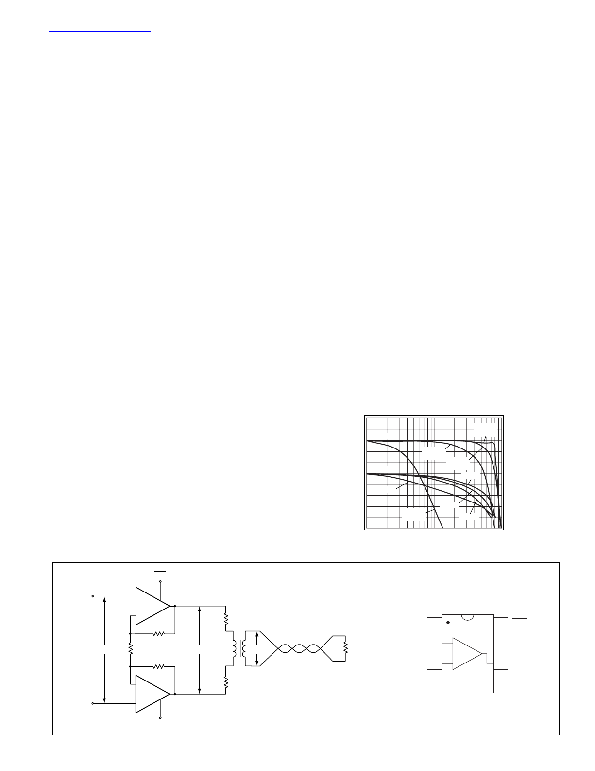
Differential Line Driver for xDSL
Pinout
DIP & SOIC
General Description
The CLC5665 is a low-cost, wideband amplifier that provides very
low 2nd and 3rd harmonic distortion at 1MHz (-89/-92dBc). The
great slew rate of 1800V/µs, bandwidth of 90MHz (Av= +1) and
fast disable make it an excellent choice for many high speed
multiplexing applications. Like all current feedback op amps, the
CLC5665 allows the frequency response to be optimized
(or adjusted) by the selection of the feedback resistor. For
demanding video applications, the 0.1dB bandwidth to 20MHz
and differential gain/phase of 0.05%/0.05° make the CLC5665
the preferred component for broadcast quality NTSC and PAL
video systems.
The large voltage swing (28Vpp), continuous output current
(85mA) and slew rate (1800V/µs) provide high-fidelity signal
conditioning for applications such as CCDs, transmission lines
and low impedance circuits.
xDSL, video distribution, multimedia and general purpose
applications will benefit from the CLC5665’s wide bandwidth and
disable feature.Power is reduced and the output becomes a high
impedance when disabled. The wide gain range of the CLC5665
makes this general purpose op amp an improved solution for
circuits such as active filters, single-to-differential-ended dr ivers,
DAC transimpedance amplifiers and MOSFET drivers.
CLC5665
Low Distortion Amplifier with Disable
N
June 1999
CLC5665
Low Distortion Amplifier with Disable
© 1999 National Semiconductor Corporation http://www.national.com
Printed in the U.S.A.
查询CLC5665供应商
Non-Inverting Frequency Response
Av = 1
= 698
R
Av = 2
= 604
f
f
Av = 1
Av = 10
Gain
Phase
Av = 50
Magnitude (1dB/div)
Av = 50
= 500
R
f
Av = 10
= 100
R
f
R
Av = 2
Phase (deg)
0
-45
-90
-135
-180
1
DIS
+
V
in (Vpp
-
+
CLC5665
R
f1
604Ω
R
g
) Vo = 2V
1.2kΩ
R
f2
604Ω
-
CLC5665
+
DIS
R
o
1:n
in
R
o
nV
o
Note: Supply and Bypassing not shown.
R
L
V
non-inv
-V
10
Frequency (MHz)
NC
1
V
2
inv
3
4
cc
100
DIS
8
-
+
+V
7
cc
V
6
out
NC
5
http://www.national.com 2
PARAMETERS CONDITIONS V
cc
TYP MIN/MAX RATINGS UNITS NOTES
Ambient Temperature CLC5665 +25°C +25°C 0 to 70°C -40 to 85°C
FREQUENCY DOMAIN RESPONSE
small-signal bandwidth (A
v
= +1) V
out
< 1.0V
pp
±15 90 MHz
small-signal bandwidth V
out
< 1.0V
pp
±15 70 MHz
V
out
< 1.0V
pp
±5 50 MHz
0.1dB bandwidth V
out
< 1.0V
pp
±15 20 MHz
V
out
< 1.0V
pp
±5 15 MHz
large-signal bandwidth V
out
= 10V
pp
25 MHz
gain flatness V
out
< 1.0V
pp
peaking DC to 10MHz 0.03 dB
rolloff DC to 20MHz 0.1 dB
linear phase deviation DC to 20MHz 0.7 deg
differential gain 4.43MHz, R
L
= 150Ω ±15 0.05 %
4.43MHz, R
L
= 150Ω ±5 0.05 %
differential phase 4.43MHz, R
L
= 150Ω ±15 0.05 deg
4.43MHz, R
L
= 150Ω ±5 0.1 deg
TIME DOMAIN RESPONSE
rise and fall time 2V step 5 ns
10V step 10 ns
settling time to 0.05% 2V step 35 ns
overshoot 2V step 5 %
slew rate 20V step 1800 V/µs
DISTORTION AND NOISE RESPONSE
2nd harmonic distortion 1Vpp,1MHz, RL = 500Ω -89 dBc
3rd harmonic distortion 1V
pp
,1MHz, RL = 500Ω -92 dBc
input voltage noise >1MHz 3.0 nV/√Hz
non-inverting input current noise >1MHz 3.2 pA/√Hz
inverting input current noise >1MHz 15 pA/√Hz
DC PERFORMANCE
input offset voltage ±15 1.0 7.5 9.0 10.0 mV A
average drift 25 – µV/°C
input bias current non-inverting ±15, ±5 3 20 20 20 µAA
average drift 10 – nA/°C
input bias current inverting ±15, ±5 3 20 20 20 µAA
average drift 10 – nA/°C
power-supply rejection ratio DC 60 55 50 50 dB
common-mode rejection ratio DC 60 55 50 50 dB
supply current R
L
= ∞ ±15, ±5 11, 8.5 12 14 15 mA A
disabled R
L
= ∞ ±15, ±5 1.5 2.5 2.5 2.5 mA A
SWITCHING PERFORMANCE
turn on time 400 500 550 550 ns
turn off time (Note 2) 200 800 800 800 ns
off isolation 10MHz 59 56 56 56 dB
high input voltage V
IH
±15 11.8 12.5 12.7 V
±5 1.8 2.5 2.7 V
low input voltage V
IL
±15 10.8 10.5 10.0 V
±5 0.8 0.6 0.1 V
MISCELLANEOUS PERFORMANCE
non-inverting input resistance 8.0 3.0 2.5 1.7 MΩ
non-inverting input capacitance 0.5 1.0 1.0 1.0 pF
input voltage range common mode ±15 ±12.5 ±12.3 ±12.1 ±11.8 V
common mode ±5 ±2.5 ±2.3 ±2.2 ±1.9 V
output voltage range R
L
= ∞ ±15 ±14 ±13.7 ±13.7 ±13.6 V
R
L
= ∞ ±5 ±4.0 ±3.9 ±3.8 ±3.7 V
output current ±85 ±60 ±50 ±45 mA
Min/max ratings are based on product characterization and simulation. Individual parameters are tested as noted. Outgoing quality levels are
determined from tested parameters.
CLC5665 Electrical Characteristics
(VCC= ±15V, Av= +2V/V; Rf= 604Ω,RL= 100Ω; unless specified)
Absolute Maximum Ratings
supply voltage
±
16V
short circuit current (see note 1)
common-mode input voltage
±
V
CC
maximum junction temperature +150°C
storage temperature range -65°C to +150°C
lead temperature (soldering 10 sec) +300°C
Notes
A) J-level: spec is 100% tested at +25°C.
1) Output is shor t circuit protected to ground, however
maximum reliability is obtained if output current does not
exceed 125mA.
2) To >50dB attenuation @ 10MHz.
3 http://www.national.com
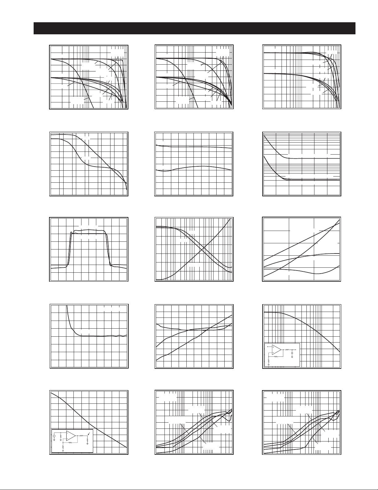
CLC5665 T ypical Performance
(VCC= ±15V, Av= +2V/V; Rf= 604Ω,RL= 100Ω; unless specified)
Non-Inverting Frequency Response
Gain
Av = 10
= 100
R
f
Av = 2
= 604
R
Phase
Av = 50
Magnitude (1dB/div)
Av = 50
= 500
R
f
1
f
Av = 2
10
Frequency (MHz)
Open-Loop Transimpedance Gain (Zs)
130
120
Gain
110
100
90
Phase
80
70
Gain (20 log)
60
50
40
30
0.0001 0.001 0.01 1 10
0.1
Frequency (MHz)
Signal Pulse Response
Large Signal
Small Signal
Large Signal Output (2V/div)
Time (20ns/div)
Short Term Settling Time
0.2
0.15
2V output step
0.1
0.05
Short Term
0
-0.05
Settling Error (%)
-0.1
-0.15
-0.2
-1dBm Compression to Load
26
Time (10ns/div)
24
22
20
18
16
14
12
V
in
10
Compression Point (dBm)
8
698Ω
698Ω
Load
50Ω
50Ω
6
0 5 10 15 20 25 30 35 40 45 50
Frequency (MHz)
Av = 1
Av = 10
Av = 1
R
= 698
f
Phase (deg)
0
-45
-90
-135
-180
100
0
20
Phase (deg)
40
60
80
100
120
140
160
100
70
Small Signal Output (0.5V/div)
60
50
40
30
20
PSRR/CMRR (dB)
10
7.0
6.0
5.0
4.0
3.0
2.0
(mV)
OS
1.0
V
-1.0
-2.0
-3.0
-10
-20
-30
-40
-50
-60
-70
-80
Distortion Level (dBc)
-90
-100
Inverting Frequency Response
Av = -1
= 500
R
Gain
Phase
Av = -50
Magnitude (1dB/div)
Av = -50
= 2.5k
R
f
1
Av = -10
= 500
R
f
10
Av = -2
= 500
R
f
Av = -10
Av = -2
f
Av = -1
Frequency (MHz)
Flatness Gain and Linear Phase
Gain
Phase
Magnitude (0.1dB/div)
0481216
Frequency (MHz)
PSRR, CMRR and Closed Loop R
CMRR
PSRR
20 log R
o
0
0.01 0.10 1 10
o
Frequency (MHz)
IBI, IBN. VOS vs. Temperature
I
BN
I
BI
0
V
OS
-60 -20 20 60 100
Temperature (°C)
Harmonic Distortion vs. Frequency
0
RL = 100Ω
V
= 2V
out
pp
2nd
VCC = ±5V
2nd
VCC = ±15V
3rd
VCC = ±5V
3rd
VCC = ±15V
1 10 100
Frequency (MHz)
100
20
100
140
Phase (deg)
0
-45
-90
-135
-180
Phase (0.2°/div)
Noise Voltage (nV/√Hz)
30
20
0.08
10
20 log R
0.06
0
-10
o
0.04
Gain (%)
-20
0.02
-30
-40
5.0
4.5
4.0
3.5
I
BI
, I
3.0
BN
2.5
(µA)
2.0
1.5
Intercept (+dBm)
1.0
0.5
0
Distortion Level (dBc)
-100
Frequency Response vs. Load
Gain
RL = 50
Phase
Magnitude (1dB/div)
1
RL = 100
RL = 1k
RL = 50
RL = 100
10
Frequency (MHz)
Equivalent Input Noise
100
Inverting Current 14.8pA/√Hz
10
Non-Inverting Current 3.2pA/√Hz
Voltage 3.0nV/√Hz
1
0.1k 1k 10k 100k 1M
10M
Frequency (MHz)
Differential Gain and Phase (3.58MHz)
1
Gain Negative Sync
Phase
Positive Sync
Phase Negative Sync
Gain Positive Sync
0
123
Number of 150Ω Loads
2-Tone, 3rd Order Intermodulation Intercept
60
50
40
30
20
10
50Ω
P
out
750Ω
750Ω
50Ω
6
10
7
10
Frequency (MHz)
Harmonic Distortion vs. Frequency
0
RL = 500Ω
-10
V
= 2V
out
-20
-30
-40
-50
pp
2nd
VCC = ±15V
2nd
VCC = ±5V
-60
-70
-80
-90
VCC = ±15V
3rd
VCC = ±5V
1 10 100
Frequency (MHz)
RL = 1k
Phase (deg)
0
-45
-90
-135
-180
100
Noise Current (pA/√Hz)
100M
0.30
0.24
Phase (deg)
0.18
0.12
0.06
0.03
4
3rd

http://www.national.com 4
The CLC5665 is a general purpose current-feedback
amplifier for use in a variety of small- and large-signal
applications. Use the feedback resistor to fine tune the
gain flatness and -3dB bandwidth for any gain setting.
National provides information for the performance at a
gain of +2 for small and large signal bandwidths. The
plots show feedback resistor values for selected gains.
Gain
Use the following equations to set the CLC5665’s noninverting or inverting gain:
Choose the resistor values for non-inverting or inverting
gain by the following steps.
Figure 1: Component Identification
1) Select the recommended feedback resistor Rf.
2) Choose the value of Rgto set gain.
3) Select Rsto set the circuit output impedance.
4) Select Rinfor input impedance and input bias.
High Gains
Current feedback closed-loop bandwidth is independent
of gain-bandwidth-product for small gain changes. For
larger gain changes the optimum feedback register Rfis
derived by the following:
Rf= 724Ω – 60Ω•(Av)
As gain is increased, the feedback resistor allows bandwidth to be held constant over a wide gain range. For a
more complete explanation refer to application note O A-25:
Stability Analysis of Current-Feedback Amplifiers
.
Resistors have varying parasitics that affect circuit
performance in high-speed design. For best results, use
leaded metal-film resistors or surface mount resistors. A
SPICE model for the CLC5665 is available to simulate
overall circuit perfor mance.
Enable/Disable Function
The CLC5665 amplifier features an enable/disable
function that changes the output and inverting input from
low to high impedance. The pin 8 enable/disable logic
levels are as follows:
V
CC
±15V ±5V
Enable >12.7V >2.7V
Disable <10.0V <0.8V
The amplifier is enabled with pin 8 left open due to the
2kΩ pull-up resistor, shown in Figure 2.
Figure 2: Pin 8 Equivalent Disable Circuit
Open-collector or CMOS interfaces are recommended to
drive pin 8. The turn-on and off time depends on the
speed of the digital interface.
The equivalent output impedance when disabled is
shown in Figure 3. With Rgconnected to ground, the sum
of Rfand Rgdominates and reduces the disabled output
impedance. To raise the output impedance in the disabled state, connect the CLC5665 as a unity-gain
voltage follower by removing Rg. Current-feedback
op-amps need the recommended Rfin a unity-gain
follower circuit. For high density circuit layouts consider
using the dual CLC431 (with disable) or the dual CLC432
(without disable).
Figure 3: Equivalent Disabled Output Impedance
Non Inverting Gain 1
R
R
InvertingGain
-R
R
f
g
f
g
−=+
=
CLC5665 Design Considerations
+V
cc
2kΩ
To CLC5665
Bias network
8kΩ
-V
Pin 8 DISABLE
cc
V
in
R
+
CLC5665
in
-
R
f
R
g
R
V
s
o
Equivalent Impedance
in Disable
Ω
V
out
R
f
100k
(Ω)
out
Z
1M
10k
1k
100
V
in
+
300k
8pF
-
R
g
10
1
1
10
Frequency (MHz)
100

2nd and 3rd Harmonic Distortion
To meet low distortion requirements, recognize the effect
of the feedback resistor. Increasing the feedback
resistor will decrease the loop gain and increase
distortion. Decreasing the load impedance increases 3rd
harmonic distortion more than 2nd.
Differential Gain and Differential Phase
The CLC5665 has low DG and DP errors for video
applications. Add an external pulldown resistor to the
CLC5665’s output to improve DG and DP as seen in
Figure 4. A 604Ω Rpwill improve DG and DP to 0.01%
and 0.02°.
Figure 4: Improved DG and DP Video Amplifier
Printed Circuit Layout
To get the best amplifier performance careful placement
of the amplifier, components and printed circuit traces
must be observed. Place the 0.1µF ceramic decoupling
capacitors less than 0.1” (3mm) from the power supply
pins. Place the 6.8µF tantalum capacitors less than
0.75” (20mm) from the power supply pins.Shorten traces
between the inverting pin and components to less
than 0.25” (6mm). Clear ground plane 0.1” (3mm) away
from pads and traces that connect to the inverting, noninverting and output pins. Do not place ground or power
plane beneath the op-amp package. National provides
literature and evaluation boards CLC730013 DIP or
CLC730027 SOIC illustrating the recommended op-amp
layout.
Level Shifting
The circuit shown in Figure 5 implements lev el shifting by
AC coupling the input signal and summing a DC voltage.
The resistor Rinand the capacitor C set the high-pass
break frequency. The amplifier closed-loop bandwidth is
fixed by the selection of Rf. The DC and AC gains for
circuit of Figure 5 are different.The AC gain is set by the
ratio of Rf and Rg. And the DC gain is set by the parallel
combination of Rgand R2.
Figure 5: Level Shifting Circuit
Multiplexing
Multiple signal switching is easily handled with the disable function of the CLC5665. Board trace capacitance
at the output pin will affect the frequency response and
switching transients. To lessen the effects of output
capacitance place a resistor (Ro) within the feedback
loop to isolate the outputs as shown in Figure 6.To match
the mux output impedance to a transmission line, add a
resistor (Rs) in series with the output.
Figure 6: Output Connection for
Multiplexing Circuits
Differential Line Driver With Load
Impedance Conversion
The circuit shown in Figure 7, operates as a differential
line driver. The tr ansformer converts the load impedance
to a value that best matches the CLC5665’s output
capabilities. The single-ended input signal is converted
to a differential signal by the CLC5665. The line’s
characteristic impedance is matched at both the input
and the output.The schematic shows Unshielded Twisted
Pair f or the transmission line;other types of lines can also
be driven.
Figure 7: Differential Line Driver with
Load Impedance Conversion
5 http://www.national.com
Applications Circuits
Add R to
p
improve
V
in
R
in
+
CLC5665
DG and DP
V
out
R
s
-
V
in
AC
C
+
R
in
CLC5665
V
out
-
V
in
DC
R
2
R
R
g
f
R
R
R
g
f
p
-V
cc
VV
=+
out in
ac
1
RR
R
f
−
g
22
R
V
in
f
DC
R
CLC5665
+
+
CLC5665
-
g
R
DIS1
DIS2
R
f
R
o
V
R
R
o
f
out
s
R
L
R
g
V
in1
V
R
in2
in
R
in
R
R
g2
+
CLC5665
-
V
R
f1
V
in
R
t1
R
g1
R
f2
d/2
R
-
CLC5665
+
R
t2
m/2
-V
d/2
1:n
R
eq
R
m/2
Z
UTP
I
o
o
+
R
V
L
o
-

http://www.national.com 6
Set up the CLC5665 as a difference amplifier. Vdis
determined by:
Make the best use of the CLC5665’s output drive
capability as follows:
where Reqis the transformed value of the load impedance, V
max
is the Output Voltage Range, and I
max
is the
maximum Output Current.
Match the line’s characteristic impedance:
Select the transformer so that it loads the line with a
value very near Zoover frequency range. The output
impedance of the CLC5665 also affects the match. With
an ideal transformer we obtain:
where Z
o(5665)
(jω) is the output impedance of the
CLC5665 and |Z
o(5665)
(jω)| << Rm.
The load voltage and current will fall in the ranges:
The CLC5665’s high output drive current and low
distortion make it a good choice for this application.
Full Duplex Cable Driver
The circuit shown in Figure 8 below, operates as a full
duplex cable driver which allows simultaneous transmission and reception of signals on one transmission line.
The circuit on either side of the transmission line uses are
CLC5665 as a cable driver, and the second CLC5665 as
a receiver. VoAis an attenuated version of V
inA
, while V
oB
is an attenuated version of V
inB
.
Figure 8: Full Duplex Cable Driver
R
m1
is used to match the transmission line. Rf2and R
g2
set the DC gain of the CLC5665, which is used in a
difference mode. Rt2provides good CMRR and DC
offset. The transmitting CLC5665’s are shown in a unity
gain configuration because they consume the least
power of any gain, for a given load. For proper operation
we need Rf2= Rg2.
The receiver output voltages are:
where A is the attenuation of the cable, Z
o(5665)
(jω) is
the output impedance of the CLC5665, and |Z
o(5665)
(jω)|
<< Rm1.
We selected the component values as follows:
■
Rf1= 1.2kΩ, the recommended value for
CLC5665 at unity gain
■
Rm1= Zo= 50Ω, the characteristic impedance
of the transmission line
■
Rf2= Rg2= 750Ω ≥ Rm1, the recommended
value for the CLC5665 at Av = 2
■
These values give excellent isolation from the other input:
The CLC5665 provides large output current drive, while
consuming little supply current, at the nominal bias point.
It also produces low distortion with large signal swings
and heavy loads. These features make the CLC5665 an
excellent choice for driving transmission lines.
V
V
21
R
R
2
R
R
d
in
f1
g1
f2
g2
=⋅+
=⋅
RR
2V
I
meq
max
max
+=
⋅
RZ
RR
n
R
R
Lo
meq
L
eq
=
=
=
ReturnLoss 20 log
nZ j
Z
,dB
10
2
o 5665
o
=− ⋅
⋅
()
()
ω
VnV
I
I
n
o
o
≤⋅
≤
max
max
V
inA
R
t1
+
CLC5665
-
Z
R
m1
0
R
m1
+
CLC5665
-
V
inB
R
t1
R
f1
R
g2
R
f2
V
oB
CLC5665
-
R
t2
+
R
R
f1
R
g2
R
f2
-
CLC5665
t2
+
V
oA
inB(A)
2
1
Z(j)
R
R
g2
o(5665)
f2
VVA
outA(B) inA(B)
≈⋅+⋅−+
V
R
m1
ω
R
R(R||R)–
==Ω
t2
f2
g2
m1
2
25
V
oA(B)
≈− =
V
inB(A)
38dB, f 5.0MHz

7 http://www.national.com
CCD Clock Driver
Figure 9: CCD Clock Driver
Reliability Information
Transistor Count 38
Pac kage Thermal Resistance
Package
θθ
JC
θθ
JA
Plastic (IN) 65°C/W 130°C/W
Surface Mount (IM) 50°C/W 145°C/W
Ordering Information
Model Temperature Range Description
CLC5665IN -40°C to +85°C 8-pin PDIP
CLC5665IM -40°C to +85°C 8-pin SOIC
CLC5665IMX -40°C to +85°C 8-pin SOIC tape and reel
V
in
R
V
offset
RR
+
CLC5665
T
-
f
R
g
R
V
s
o
C
L
14
10
6
2
-2
-6
Output Voltage (2V/div)
-10
-14
0
50 150
100
Frequency (ns)
200

http://www.national.com 8
CLC5665
Low Distortion Amplifier with Disable
Customer Design Applications Support
National Semiconductor is committed to design excellence. For sales, literature and technical support, call the
National Semiconductor Customer Response Group at 1-800-272-9959 or fax 1-800-737-7018.
Life Support Policy
National’s products are not authorized for use as critical components in life support devices or systems without the express written approval of
the president of National Semiconductor Corporation. As used herein:
1. Life support devices or systems are devices or systems which, a) are intended for surgical implant into the body, or b) support or
sustain life, and whose failure to perform, when proper ly used in accordance with instructions for use provided in the labeling, can
be reasonably expected to result in a significant injury to the user.
2. A critical component is any component of a life support device or system whose failure to perform can be reasonably expected to
cause the failure of the life support device or system, or to affect its safety or effectiveness.
National Semiconductor National Semiconductor National Semiconductor National Semiconductor
Corporation Europe Hong Kong Ltd. Japan Ltd.
1111 West Bardin Road Fax: (+49) 0-180-530 85 86 2501 Miramar Tower Tel: 81-043-299-2309
Arlington, TX 76017 E-mail: europe.support.nsc.com 1-23 Kimberley Road Fax: 81-043-299-2408
Tel: 1(800) 272-9959 Deutsch Tel: (+49) 0-180-530 85 85 Tsimshatsui, Kowloon
Fax:1(800) 737-7018 English Tel:(+49) 0-180-532 78 32 Hong Kong
Francais Tel:(+49) 0-180-532 93 58 Tel: (852) 2737-1600
Italiano Tel: (+49) 0-180-534 16 80 Fax: (852) 2736-9960
National does not assume any responsibility for use of any circuitry described, no circuit patent licenses are implied and National reserves the right at any time without notice to change said
circuitry and specifications.
N
 Loading...