

查询CLC111供应商
CLC111
Ultra High Slew Rate, Closed Loop Buffer
General Description
The CLC111 is a high performance, closed loop, monolithic
buffer designed for applications requiring very high
frequency signals.The CLC111’shigh performance includes
an extremely fast 800MHz small signal bandwidth (0.5
and an ultra high (3500V/µs) slew rate while requiring only
10.5mA quiescent current. Signal fidelity is maintained with
low harmonic distortion (−62dBc 2nd and 3rd harmonics at
20MHz). These performance characteristics are for a
demanding 100Ω load.
Featuring a patented closed loop design, the CLC111 offers
nearly ideal unity gain (0.996) with a very low (1.4Ω) output
impedance. The CLC111 is ideally suited for buffering video
signals with its 0.15%/0.04˚ differential gain and phase
performance at 4.43MHz. Power sensitive applications will
benefit from the CLC111’sexcellentperformance on reduced
or single supply voltages.
Constructed using an advanced, complementary bipolar
process and National’s proven high performance
architectures, the CLC111 is available in several versions to
meet a variety of requirements.
Enhanced Solutions (Military/Aerospace)
SMD Number: contact factory
Space level versions also available.
For more information, visit http://www.national.com/mil
n Very low output impedance (1.4Ω)
n Low (−62dBc) 2nd/3rd harmonics
n 60mA output current (
n Single supply operation (0 to 3V supply min.)
n Evaluation boards and Spice models
pp)
Applications
n Video switch buffers
n Test point drivers
n High frequency active filters
n Wideband DC clamping buffer
n High-speed peak detector circuits
@
20MHz
±
5 supplies)
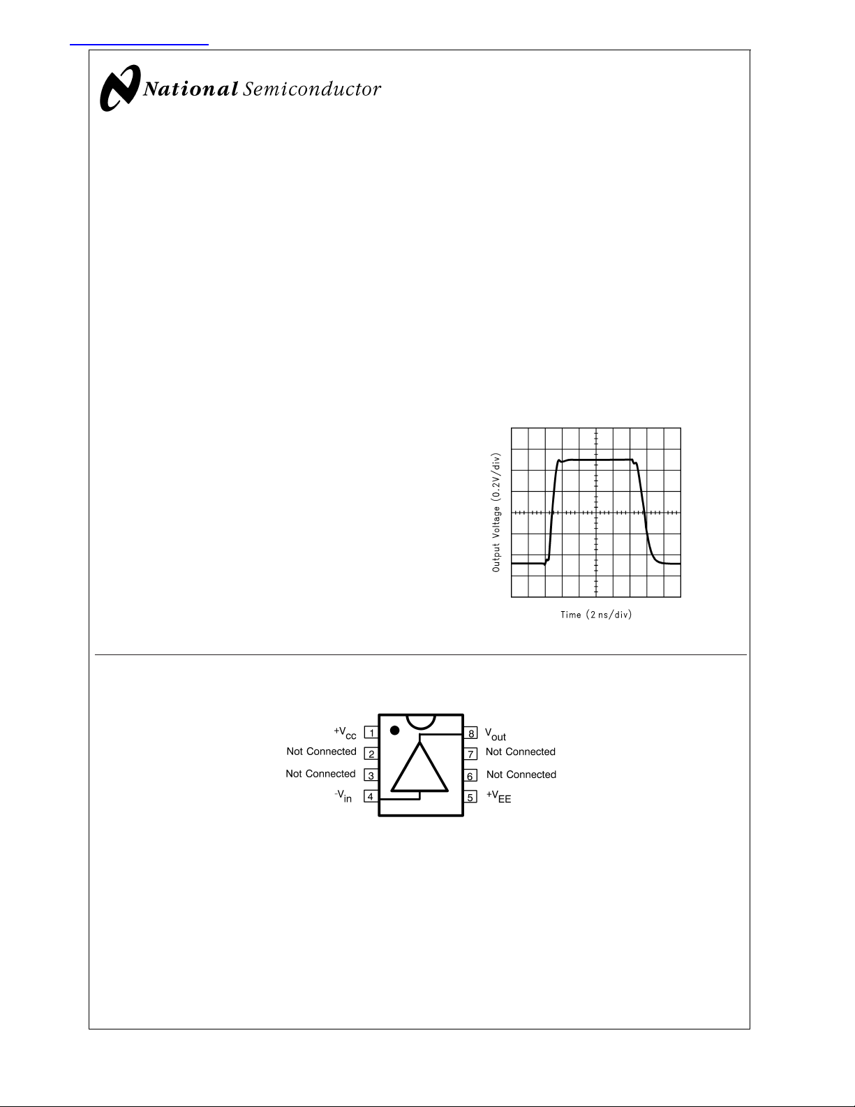
Pulse Response for±5V
CLC111 Ultra High Slew Rate, Closed Loop Buffer
February 2001
Features
n Very wideband (800MHz)
n Ultra high (3500V/µs) slew rate
Connection Diagram
DS012720-1
DS012720-2
Pinout
DIP & SOIC
© 2001 National Semiconductor Corporation DS012720 www.national.com
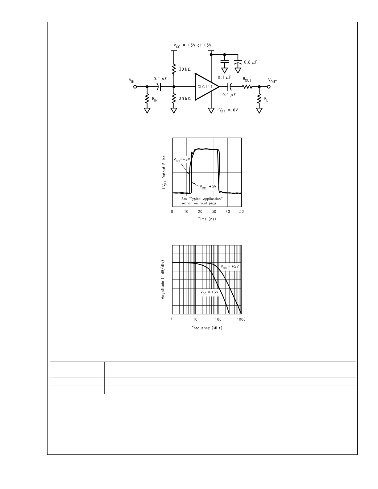
Typical Application
CLC111
DS012720-4
Single-Supply Circuit
DS012720-16
Pulse Response
DS012720-5
Small Signal Bandwidth
Ordering Information
Package Temperature Range
Industrial
8-pin plastic DIP −40˚C to +85˚C CLC111AJP CLC111AJP N08E
8-pin plastic SOIC −40˚C to +85˚C CLC111AJE CLC111AJE M08A
Part Number Package
Marking
NSC
Drawing
www.national.com 2
CLC111
Absolute Maximum Ratings (Note 1)
If Military/Aerospace specified devices are required,
please contact the National Semiconductor Sales
Office/Distributors for availability and specifications.
Supply Voltage (V
I
OUT
Output is short circuit protected to
)
CC
ground, but maximum reliability will
be maintained if I
exceed... 80mA
OUT
does not
Input Voltage
±
±
7.0V
V
CC
Operating Temperature Range 40˚C to +85˚C
Storage Temperature Range −65˚C to +150˚C
Lead Solder Duration (+300˚C) 10 sec
ESD rating 1000V
Operating Ratings
Thermal Resistance
Package (θ
)(θ
JC
MDIP 70˚C/W 125˚C/W
SOIC 65˚C/W 145˚C/W
)
JA
Maximum Junction Temperature
Range +150˚C
Electrical Characteristics
±
VCC=±5V, RL= 100Ω; unless specified
Symbol Parameter Conditions Typ Min/Max Ratings (Note 2) Units
Ambient Temperature CLC111AJ +25˚C −40˚C +25˚C +85˚C
Frequency Domain Response
SSBW Small Signal Bandwidth V
LSBW Small Signal Bandwidth V
Gain Flatness V
GFL Flatness DC-50MHz 0.02
GFPH Peaking DC-200MHz 0.1 1.0 0.5 0.5 dB
GFRH Rolloff DC-200MHz 0.1 0.8 0.8 1.2 dB
DG Differential Gain R
DP Differential Phase R
Time Domain Response
TRS Rise and Fall Time 0.5V step 0.6 0.8 0.8 1.1 ns
TRL 4.0V step 1.0 1.4 1.4 1.7 ns
TS Settling Time to
±
0.1% 2.0V Step 16 20 20 20 ns
OS1 Overshoot 4V Step 0 8 5 5 %
SR Slew Rate 4V Step 3500 2700 2700 2300 V/µsec
Distortion And Noise Performance
HD2 2nd Harmonic Distortion 2V
HD3 3rd Harmonic Distortion 2V
Equivalent Output Noise
VN Voltage
<
OUT
OUT
OUT
= 150Ω,
L
0.5V
PP
<
4.0V
PP
<
0.5V
PP
800 400 400 300 MHz
450 250 250 200 MHz
±
0.1
±
0.1
±
0.2 dB
0.15 0.4 0.25 0.25 %
4.43MHz,
= 150Ω,
L
0.04 0.08 0.08 0.08 deg
4.43MHz
, 20MHz −62 −47 −50 −50 dBc
PP
, 20MHz −62 −55 −55 −52 dBc
PP
>
1MHz 4.0 4.8 4.8 5.3 nV/
ICN Current
>
1MHz 1.6 4.0 3.0 3.0 pA/
Static, DC Performance
GA1 Small Signal Gain No Load 0.996 0.994 0.994 0.992 V/V
GA2 Small Signal Gain 100Ω Load .98 .96 .97 .97 V/V
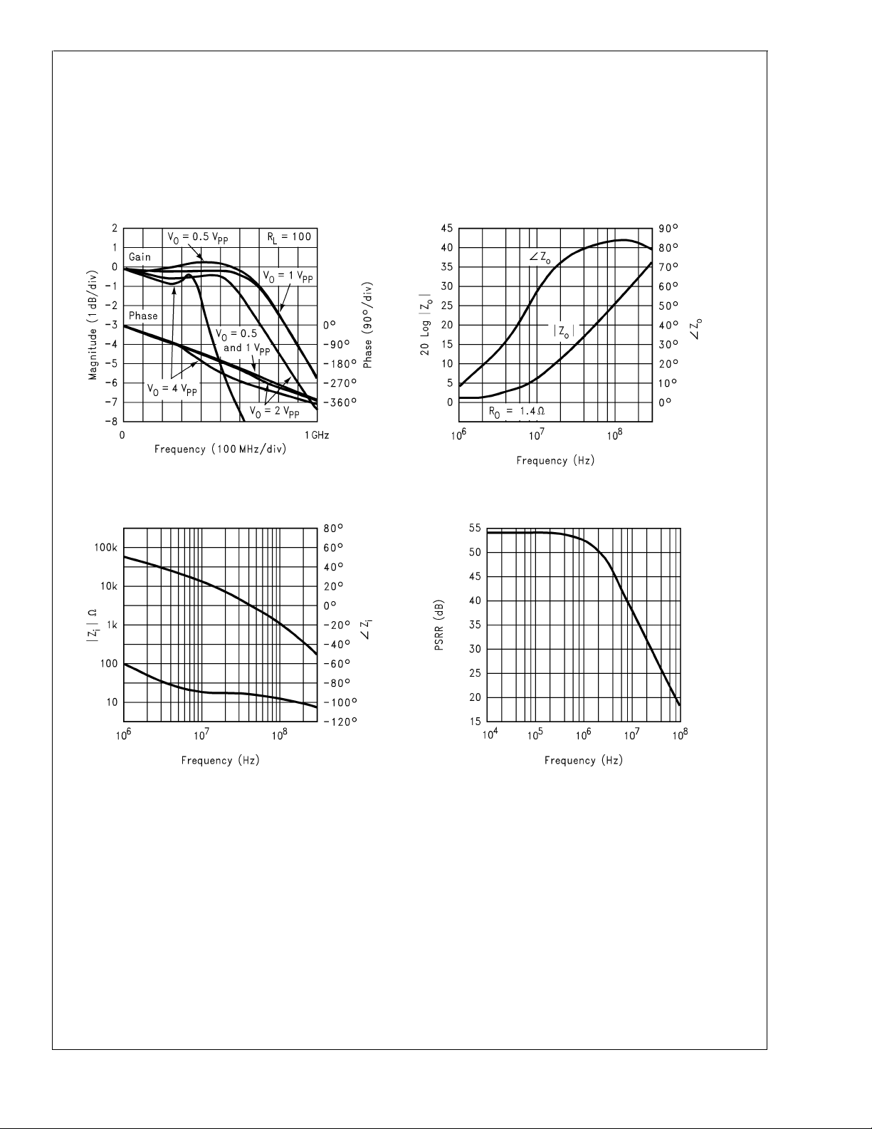
RO Output Resistance DC 1.4 3.0 2.0 2.0 Ω
VIO Output Offset Voltage (Note 3) 2 17 9 9 mV
DVIO Average Temperature
±
30
±
100 -
±
50 µV/˚C
Coefficient
IBN Input Bias Current (Note 3) 5 30 15 15 µA
DIBN Average Temperature
50
±
187 -
±
100 nA/˚C
Coefficient
PSRR Power Supply Rejection Ratio −52 −48 −48 −46 dB
www.national.com3
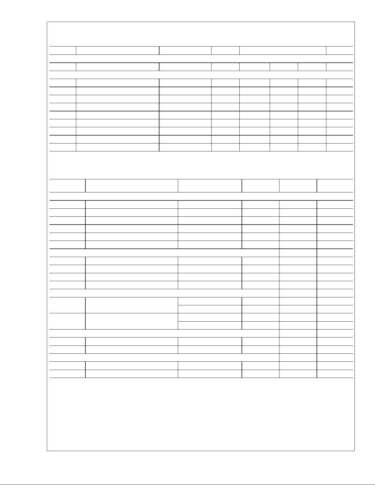
Electrical Characteristics (Continued)
±
VCC=±5V, RL= 100Ω; unless specified
CLC111
Symbol Parameter Conditions Typ Min/Max Ratings (Note 2) Units
Static, DC Performance
ICC Supply Current (Note 3) No Load 10.5 12 12 12 mA
Miscellaneous Performance
ILIN Integral Endpoint Linearity
±
2V, Full Scale 0.2 1.0 0.5 0.5 %
RIN Input Resistance 1 0.3 0.7 1 MΩ
CIN Input Capacitance CERDIP 2.5 3.5 3.5 3.5 pF
CIN Input Capacitance Plastic DIP 1.25 2.0 2.0 2.0 pF
VO Output Voltage Range No Load 3.9 3.5 3.6 3.6 V
VOL Output Voltage Range R
VOL Output Voltage Range R
= 100Ω 3.5 +3.1,−2.5 3.2 3.2 V
L
= 100Ω, 0˚C
L
±
3.1 V
IO Output Current 60 50,25 50 40 mA
IO Output Current 0˚-70˚C 50,35 50 50 mA
Electrical Characteristics
VCC=+3V or VCC=+5V, −VEE=0V, TA=+25˚C, RL=100Ω; unless specified
Symbol Parameter Conditions V
CC
=
3V
Frequency Domain Response
SSBW −3dB Bandwidth V
LSBW −3dB Bandwidth V
Gain Flatness V
OUT
OUT
OUT
<
<
<
0.5V
2.0V
0.5V
PP
PP
PP
120 300 MHz
GFL Flatness DC-30MHz 0.5 0.1 dB
GFPH Peaking DC-200MHz 0 0 dB
GFRH Rolloff DC-60MHz 1.5 0.25 dB
Time Domain Response
TRS Rise and Fall Time 0.5V step 3.9 1.2 ns
TRL Rise and Fall Time 2.0V step 1.5 ns
OS1 Overshoot 1.0V step 3 3 %
SR Slew Rate 0.5V step 260 425 V/µsec
Distortion And Noise Performance
HD2 2nd Harmonic Distortion 0.5V
HD3 3rd Harmonic Distortion 0.5V
, 20MHz −46 dBc
PP
1.0V
, 20MHz −55
PP
, 20MHz −44 dBc
PP
1.0V
, 20MHz −64
PP
Static, DC Performance
GA1 Small Signal Gain AC coupled 0.96 0.97 V/V
∞
R
=
L
2.0 4.5 mA
Miscellaneous Performance
VO Output Voltage Range R
∞
=
L
1.5 3.4 V
VOL Output Voltage Range RL= 100Ω 1.1 2.6 V
VCC=
5V
210 MHz
Units
PP
PP
www.national.com 4
Electrical Characteristics (Continued)
Note 1: “Absolute Maximum Ratings” are those values beyond which the safety of the device cannot be guaranteed. They are not meant to imply that the devices
should be operated at these limits. The table of “Electrical Characteristics” specifies conditions of device operation.
Note 2: Min/max ratings are based on product characterization and simulation. Individual parameters are tested as noted. Outgoing quality levels are determined
from tested parameters.
Note 3: AJ-level: spec. is 100% tested at +25˚C.
Typical Performance Characteristics
CLC111
Frequency Response vs. Output Swing
Input Impedance
Output Impedance
DS012720-6
DS012720-7
PSRR
DS012720-8
DS012720-9
www.national.com5
Typical Performance Characteristics (Continued)
CLC111
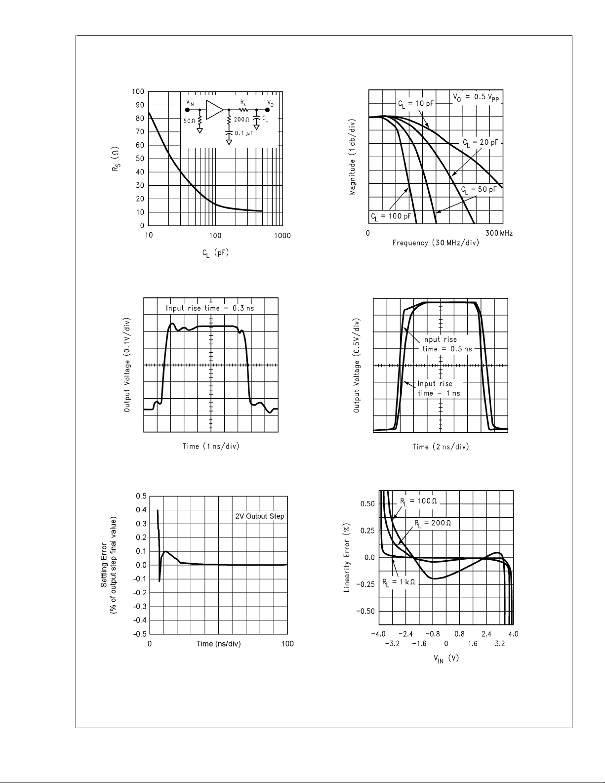
Recommended R
vs. Load Capacitance
S
DS012720-10
Gain vs. CLwith Recommended R
S
DS012720-11
Small Signal Pulse Response
Short-Term Settling Time
DS012720-12
Large Signal Pulse Response
DS012720-13
Integral Linearity Error
DS012720-14
www.national.com 6
DS012720-15
Typical Performance Characteristics (Continued)
CLC111
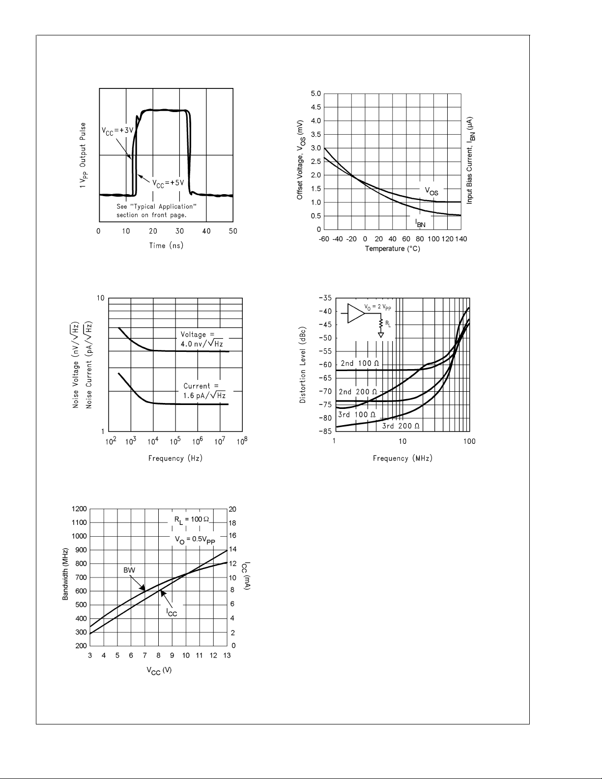
Pulse Response
Equivalent Input Noise
DS012720-16
Typical D.C. Errors vs. Temperature
DS012720-17
2nd and 3rd Harmonic Distortion
Bandwidth and ICCvs. VCC(Single Supply)
DS012720-18
DS012720-20
DS012720-19
www.national.com7
Application Division
Operation
CLC111
the CLC111 is a low-power, very high speedunity gain buffer.
It uses a closed loop topology which allows for accuracy not
usually found in high speed open loop buffers. A slew
enhanced front end allows for low quiescent power while not
sacrificing AC performance.
Single Supply Operation
Although the CLC111 is specified to operate from split
power supplies, there is no internal ground reference that
prevents operation from a single voltage power supply. For
single supply operation, the input signal should be biased at
a DC value of 1/2V
coupling and rebiasing, as shown in
The above electrical specifications provide typical
performance specifications for the CLC111 at 25˚ C while
operating from a single +3V or a single +5V power supply.
. This can be accomplished by AC
CC
Figure 1
.
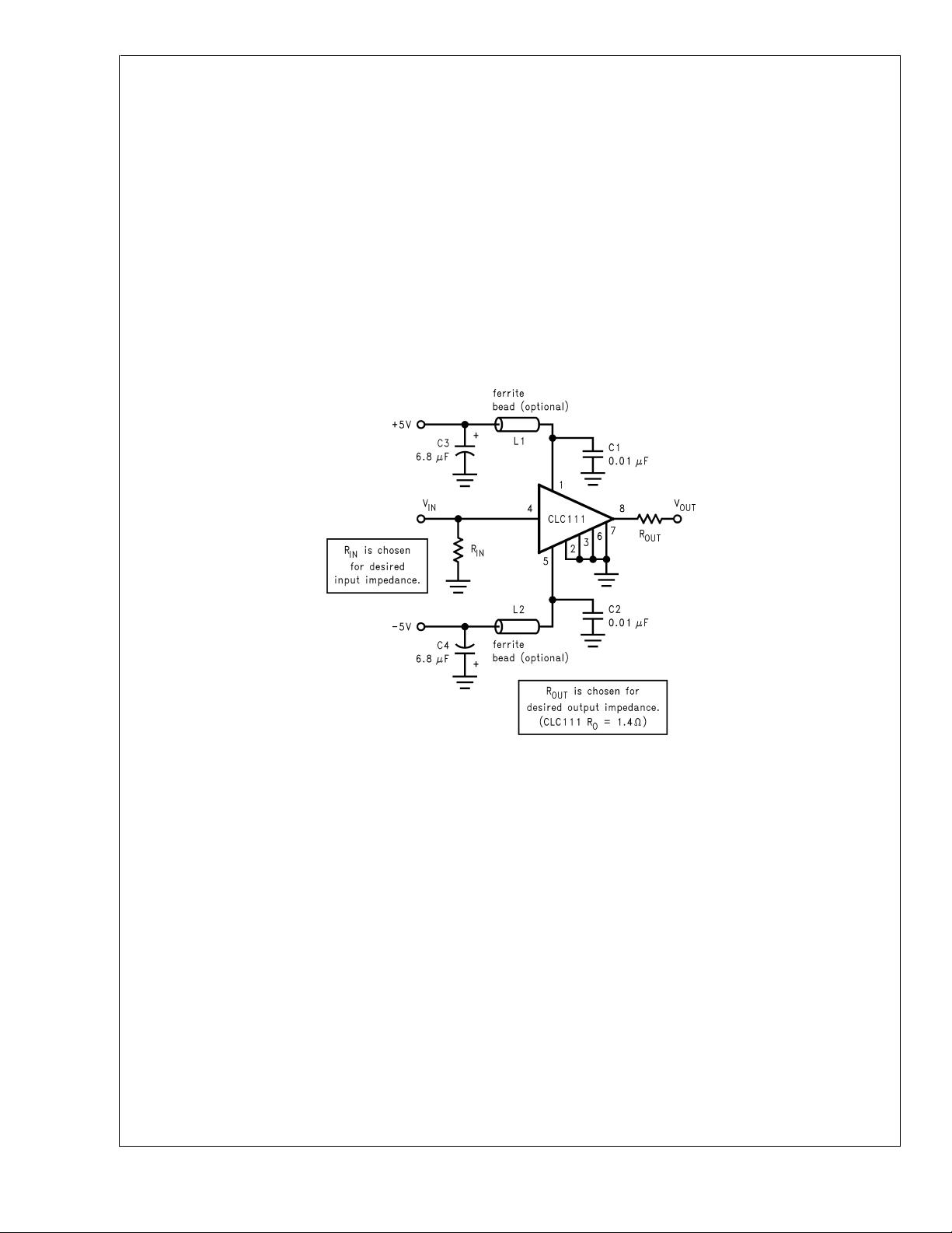
Printed Circuit Layout and Supply Bypassing
As with any high frequency device, a good PCB layout is
required for optimum performance. This is especially
important for a device as fast as the CLC111.
To minimize capacitive feedthrough, pins 2, 3, 6, and 7
should be connected to the ground plane, as shown in
Figure 1
transmission lines with the appropriate termination resistors
±
5V
very near the CLC111. On a 0.065 inch epoxy PCB material,
a 50 transmission line (commonly called stripline) can be
constructed by using a trace width of 0.01” over a complete
ground plane.
Figure 1
The ferrite beads are optional and are recommended only
where additional isolation is needed from high frequency
(
. Input and output traces should be laid out as
shows recommended power supply bypassing.
>
400MHz) resonances in the power supply.
FIGURE 1. Recommended Circuit & Evaluation Board Schematic
Parasitic or load capacitance directly on the output of the
CLC111 will introduce additional phase shift in the device.
This phase shift can decrease phase margin and increase
frequency response peaking. A small series resistor before
the capacitance effectively decouples this effect. The graphs
in this data sheetillustrate the required resistorvalueand the
resulting performance vs. capacitance.
Precision buffed resistors (PRP8351 series from Precision
Resistive Products), which have low parasitic reactances,
were used to develop the data sheet specifications.
Precision carbon composition resistors or standard
www.national.com 8
DS012720-21
spirally-trimmed RN55D metal file resistors will work, though
they will cause a slight degradation of AC performance due
to their reactive nature at high frequencies.
Evaluation Boards
Evaluation boards are available from National as part
numbers CLC730012 (DIP) and CLC730045 (SOIC). This
board was used in the characterization of the device and
provides optimal performance. Designers are encouraged to
copy these printedcircuit board layouts for their applications.

Physical Dimensions inches (millimeters) unless otherwise noted
8-Pin SOIC
NS Package Number M08A
CLC111
www.national.com9
Physical Dimensions inches (millimeters) unless otherwise noted (Continued)
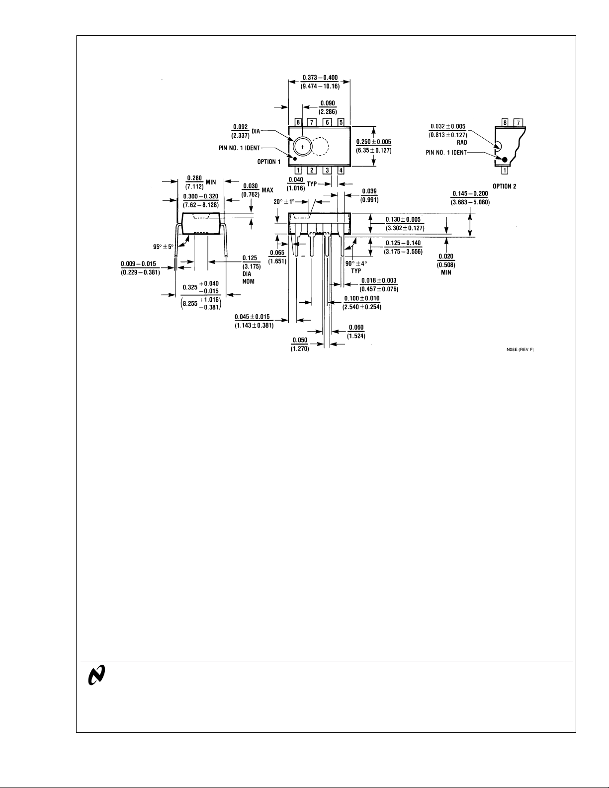
8-Pin MDIP
NS Package Number N08E
CLC111 Ultra High Slew Rate, Closed Loop Buffer
LIFE SUPPORT POLICY
NATIONAL’S PRODUCTS ARE NOT AUTHORIZED FOR USE AS CRITICAL COMPONENTS IN LIFE SUPPORT
DEVICES OR SYSTEMS WITHOUT THE EXPRESS WRITTEN APPROVAL OF THE PRESIDENT AND GENERAL
COUNSEL OF NATIONAL SEMICONDUCTOR CORPORATION. As used herein:
1. Life support devices or systems are devices or
systems which, (a) are intended for surgical implant
into the body, or (b) support or sustain life, and
whose failure to perform when properly used in
accordance with instructions for use provided in the
labeling, can be reasonably expected to result in a
significant injury to the user.
2. A critical component is any component of a life
support device or system whose failure to perform
can be reasonably expected to cause the failure of
the life support device or system, or to affect its
safety or effectiveness.
National Semiconductor
Corporation
Americas
Tel: 1-800-272-9959
Fax: 1-800-737-7018
Email: support@nsc.com
www.national.com
National does not assume any responsibility for use of any circuitry described, no circuit patent licenses are implied and National reserves the right at any time without notice to change said circuitry and specifications.
National Semiconductor
Europe
Fax: +49 (0) 180-530 85 86
Email: europe.support@nsc.com
Deutsch Tel: +49 (0) 69 9508 6208
English Tel: +44 (0) 870 24 0 2171
Français Tel: +33 (0) 1 41 91 8790
National Semiconductor
Asia Pacific Customer
Response Group
Tel: 65-2544466
Fax: 65-2504466
Email: ap.support@nsc.com
National Semiconductor
Japan Ltd.
Tel: 81-3-5639-7560
Fax: 81-3-5639-7507
 Loading...