

CLC031A
SMPTE 292M/259M Digital Video Deserializer /
Descrambler with Video and Ancillary Data FIFOs
General Description
The CLC031A SMPTE 292M / 259M Digital Video
Deserializer/Descrambler with Video and Ancillary Data
FIFOs is a monolithic integrated circuit that deserializes and
decodes SMPTE 292M, 1.485Gbps (or 1.483Gbps) serial
component video data, to 20-bit parallel data with a synchronized parallel word-rate clock. It also deserializes and decodes SMPTE 259M, 270Mbps, 360Mbps and
SMPTE 344M (proposed) 540Mbps serial component video
data, to 10-bit parallel data. Functions performed by the
CLC031A include: clock/data recovery from the serial data,
serial-to-parallel data conversion, SMPTE standard data decoding, NRZI-to-NRZ conversion, parallel data clock generation, word framing, CRC and EDH data checking and handling, Ancillary Data extraction and automatic video format
determination. The parallel video output features a variabledepth FIFO which can be adjusted to delay the output data
up to 4 parallel data clock periods. Ancillary Data may be
selectively extracted from the parallel data through the use
of masking and control bits in the configuration and control
registers and stored in the on-chip FIFO. Reverse LSB dithering is also implemented.
The unique multi-functional I/O port of the CLC031A provides external access to functions and data stored in the
configuration and control registers. This feature allows the
designer greater flexibility in tailoring the CLC031A to the
desired application. The CLC031A is auto-configured to a
default operating condition at power-on or after a reset command. Separate power pins for the PLL, deserializer and
other functional circuits improve power supply rejection and
noise performance.
The CLC031A has a unique Built-In Self-Test (BIST) and
video Test Pattern Generator (TPG). The BIST enables comprehensive testing of the device by the user. The BIST uses
the TPG as input data and includes SD and HD component
video test patterns, reference black, PLL and EQ pathologicals and a 75% saturation, 8 vertical colour bar pattern, for
all implemented rasters. The colour bar pattern has optional
transition coding at changes in the chroma and luma bar
data. The TPG data is output via the parallel data port.
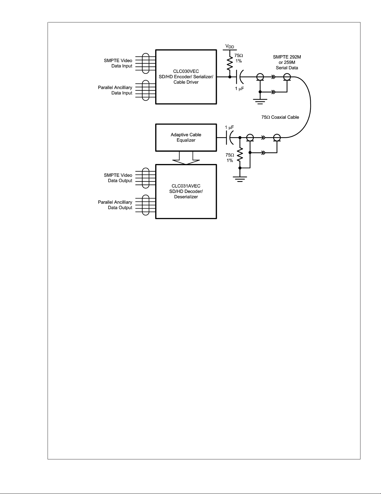
The CLC030, SMPTE 292M / 259M Digital Video Serializer
with Ancillary Data FIFO and Integrated Cable Driver, is the
ideal complement to the CLC031A.
The CLC031A’s internal circuitry is powered from +2.5 Volts
and the I/O circuitry from a +3.3 Volt supply. Power dissipation is typically 850mW. The device is packaged in a 64-pin
TQFP.
Features
n SDTV/HDTV serial digital video standard compliant
n Supports 270 Mbps, 360 Mbps, 540 Mbps, 1.483 Gbps
and 1.485 Gbps serial video data rates with
auto-detection
n LSB de-dithering option
n Uses low-cost 27MHz crystal or clock oscillator
reference
n Fast VCO lock time:
n Built-in self-test (BIST) and video test pattern generator
(TPG)*
n Automatic EDH/CRC word and flag processing
n Ancillary Data FIFO with extensive packet handling
options
n Adjustable, 4-deep parallel output video data FIFO
n Flexible control and configuration I/O port
n LVCMOS compatible control inputs and clock and data
outputs
n LVDS and ECL-compatible, differential, serial inputs
n 3.3V I/O power supply and 2.5V logic power supply
operation
n Low power: typically 850mW
n 64-pin TQFP package
n Commercial temperature range 0˚C to +70˚C
* Patent applications made or pending.
<
500 µs at 1.485 Gbps
Applications
n SDTV/HDTV serial-to-parallel digital video interfaces for:
— Video editing equipment
— VTRs
— Standards converters
— Digital video routers and switchers
— Digital video processing and editing equipment
— Video test pattern generators and digital video test
equipment
— Video signal generators
September 2004
CLC031A SMPTE 292M/259M Digital Video Deserializer / Descrambler with Video and Ancillary
Data FIFOs
Ordering Information
Order Number Package Type NS Package Number
CLC031AVEC 64-Pin TQFP VEC-64A
© 2004 National Semiconductor Corporation DS200201 www.national.com
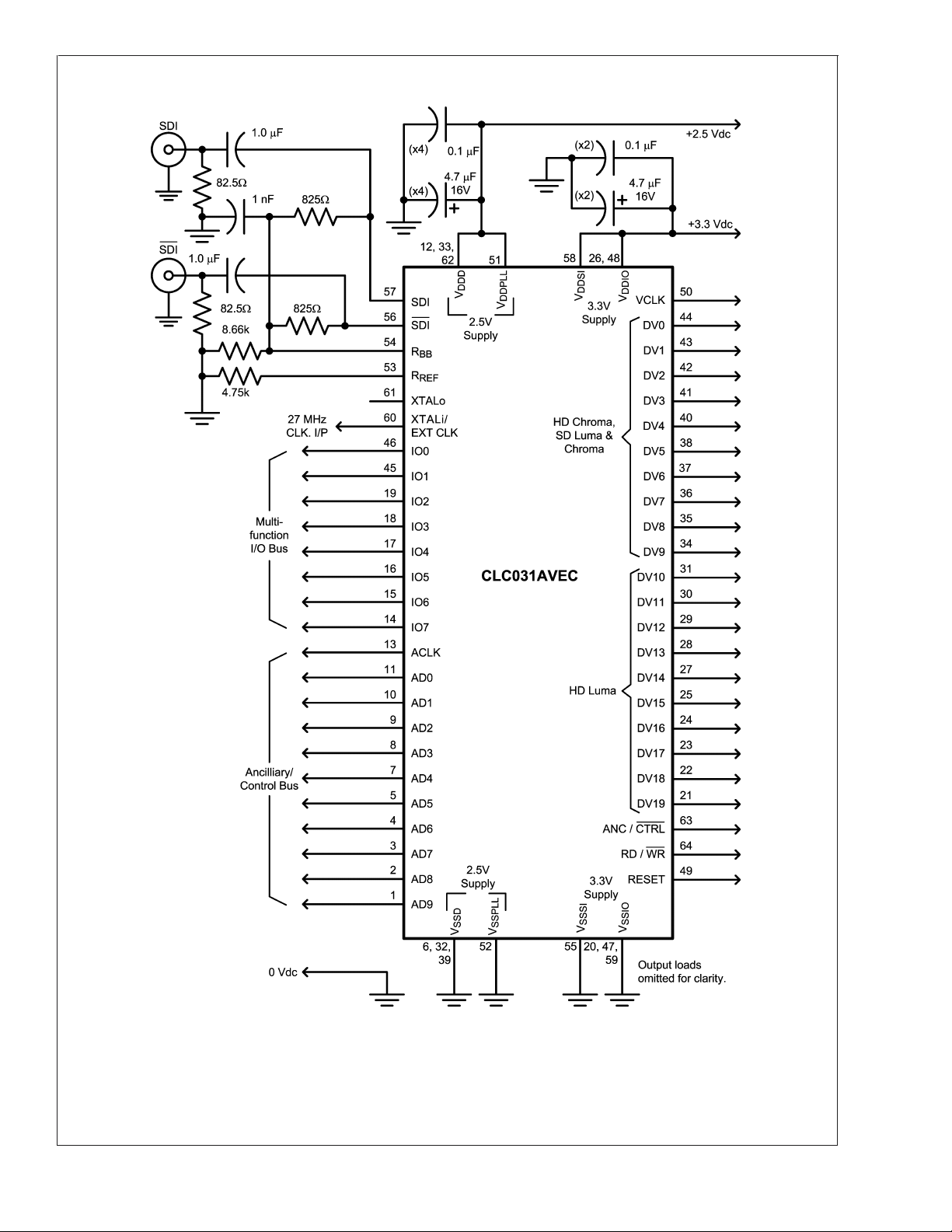
Typical Application
CLC031A
20020101
www.national.com 2
Block Diagram
CLC031A
20020102
www.national.com3
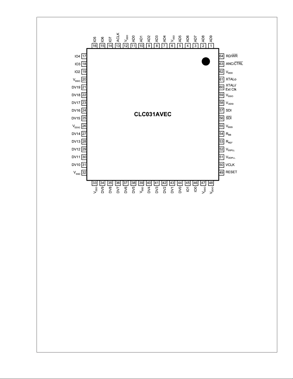
Connection Diagram
CLC031A
64-Pin TQFP
Order Number CLC031AVEC
See NS Package Number VEC-64A
20020103
www.national.com 4

CLC031A
Absolute Maximum Ratings (Note 1)
It is anticipated that this device will not be offered in
a military qualified version. If Military/Aerospace speci-
fied devices are required, please contact the National
Semiconductor Sales Office / Distributors for availability
and specifications.
CMOS I/O Supply Voltage
(V
DDIO–VSSIO
SDI Supply Voltage
(V
DDSI–VSSSI
Digital Logic Supply Voltage
(V
DDD–VSSD
PLL Supply Voltage
(V
DDPLL–VSSPLL
CMOS Input Voltage
(Vi):
CMOS Output Voltage
(Vo):
): 4.0V
): 4.0V
): 3.0V
): 3.0V
V
−0.15V to
SSIO
+0.15V
V
DDIO
V
−0.15V to
SSIO
+0.15V
V
DDIO
CMOS Input Current (single input):
Vi=V
Vi=V
CMOS Output Source/Sink Current:
I
Output Current: +300 µA
BB
I
Output Current: +300 µA
REF
SDI Input Voltage
(Vi):
−0.15V: −5 mA
SSIO
+0.15V: +5 mA
DDIO
V
SSSI
V
±
−0.15V to
+0.15V
DDSI
6mA
Package Thermal Resistance
@
θ
0 LFM Airflow 40.1˚C/W
JA
@
θ
500 LFM Airflow 24.5˚C/W
JA
θ
JC
5.23˚C/W
Storage Temp. Range: −65˚C to +150˚C
Junction Temperature: +150˚C
Lead Temperature (Soldering 4
Sec): +260˚C
ESD Rating (HBM): 6.0 kV
ESD Rating (MM): 400 V
Recommended Operating Conditions
Symbol Parameter Conditions Reference Min Typ Max Units
V
V
V
V
T
DDIO
DDSD
DDD
DDPLL
A
CMOS I/O Supply Voltage V
SDI Supply Voltage V
Digital Logic Supply
Voltage
PLL Supply Voltage V
Operating Free Air
Temperature
DDIO−VSSIO
DDSI−VSSSI
V
DDD–VSSD
DDPLL–VSSPLL
3.150 3.300 3.450 V
2.375 2.500 2.625 V
0 +70 ˚C
Required Input Conditions
(Note 9)
Symbol Parameter Conditions Reference Min Typ Max Units
V
IN
t
r,tf
BR
V
CM(SDI)
V
IN(SDI)
V
IN(SDI)
tr,t
SDI
f
Input Voltage Range
Rise Time, Fall Time 10%–90% 1.0 1.5 3.0 ns
All LVCMOS
Inputs
SMPTE 259M, Level C
V
SSIO
V
DDIO
270
SMPTE 259M, Level D 360
Serial Input Data Rate
SMPTE 344M 540
SDI, SDI
M
SMPTE 292M 1,483
SMPTE 292M 1,485
Common Mode Voltage VIN= 125 mV
SDI Serial Input Voltage,
Single-ended
SDI Serial Input Voltage,
Differential
20%–80%, SMPTE 259M
Rise Time, Fall Time
Data Rates
20%–80%, SMPTE 292M
Data Rates
P-P
SDI, SDI
V
SSSI
+1.0V
125 800 880 mV
125 800 880 mV
0.4 1.0 1.5 ns
V
DDSI
−0.05V
270 ps
V
BPS
V
P-P
P-P
www.national.com5
Required Input Conditions (Continued)
Symbol Parameter Conditions Reference Min Typ Max Units
CLC031A
f
ACLK
DC
ACLK
tr,t
f
Ancillary / Control Data
Clock Frequency
Duty Cycle, Ancillary Clock 45 50 55 %
Ancillary / Control Clock
and Data Rise Time, Fall
10%–90% 1.0 1.5 3.0 ns
A
CLK
V
CLK
Time
t
S
t
H
R
REF
f
EXT CLK
f
XTAL
Setup Time, ADNto A
or IONto A
CLK
Edge
Hold Time, Rising Edge
to ADNor A
A
CLK
IO
N
Bias Supply Reference
Resistor
External Clock Frequency Ext Clk
Crystal Frequency Figure 6 XTALo, XTALi
Rising
CLK
CLK
3.0 1.5 ns
Control Data Input or
I/O Bus Input
to
IO
,ADN,A
N
CLK
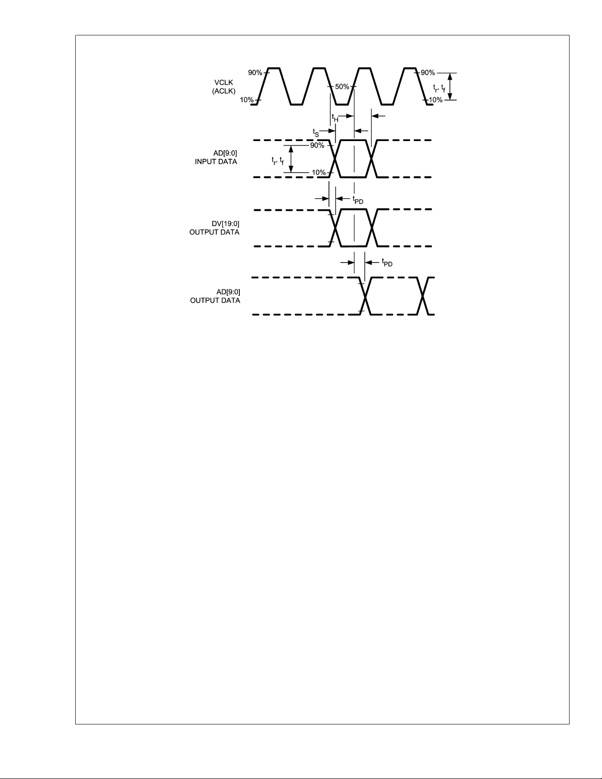
Timing Diagram
3.0 1.5 ns
Tolerance 1% 4.75k Ω
−100
ppm
27.0
+100
ppm
DC Electrical Characteristics
Over Supply Voltage and Operating Temperature ranges, unless otherwise specified (Notes 2, 3).
Symbol Parameter Conditions Reference Min Typ Max Units
V
V
I
I
V
V
V
V
V
I
V
I
I
I
I
IH
IL
IH
IL
OH
OL
OHV
OLP
SDI
SDI
TH
BB
REF
DD
DD
(3.3V)
(2.5V)
Input Voltage High Level
Input Voltage Low Level V
Input Current High Level VIH=V
Input Current Low Level VIL=V
(Note 8) +85 +150
DDIO
SSIO
All LVCMOS
Inputs
Output Voltage High Level IOH=−2mA
Output Voltage Low Level IOL=+2mA V
All LVCMOS
Outputs
Minimum Dynamic V
Maximum Dynamic V
OH
OL
IOH=−2mA
(Note 6)
IOL=+2mA
(Note 6)
Serial Data Input Voltage
Serial Data Input Current
SDI, SDI
Input Thereshold Over VCM range
Bias Supply Output
Current
Reference Output Current R
Power Supply Current,
3.3V Supply, Total
Power Supply Current,
2.5V Supply, Total
= 8.66kΩ 1% −220 −188
R
BB
= 4.75kΩ 1% −290 −262
REF
270M
1,485M
270M
1,485M
Data Rate
BPS
Data Rate 47.0 50.0
BPS
Data Rate
BPS
Data Rate 220 340
BPS
V
DDIO,VDDSI
V
DDD,VDDPLL
2.0 V
SSIO
DDIO
0.8
−1 −20
2.4 2.7 V
V
SSIO
+0.3
V
DDIO
SSIO
DDIO
V
SSIO
+0.5V
−0.5
V
SSIO
+0.4
125 800 880 mV
±
1
<
100 mV
±
10 µA
38.0 45.0
80 120
MHz
MHz
V
µA
V
P-P
µA
mA
mA
www.national.com 6
AC Electrical Characteristics
Over Supply Voltage and Operating Temperature ranges, unless otherwise specified (Note 3).
Symbol Parameter Conditions Reference Min Typ Max Units
Serial Video Data Inputs
SMPTE 259M, Level C
SMPTE 259M, Level D 360
BR
SDI
Serial Input Data Rate
SMPTE 344M 540
SMPTE 292M 1,483
SDI, SDI
0.4 1.0 1.5 pns
t
r,tf
Rise Time, Fall Time
SMPTE 292M 1,485
20%–80%, SMPTE 259M
Data Rates
20%–80%, SMPTE 292M
Data Rates
Parallel Video Data Outputs
f
VCLK
t
pd
DC
SMPTE 259M, 270M
Video Output Clock
Frequency
SMPTE 267M, 360M
SMPTE 344M, 540M
SMPTE 292M, 1,483M
SMPTE 292M, 1,485M
Propagation Delay, Video
Clock to Video Data Valid
V
Duty Cycle, Video Clock V
50%–50%
BPS
BPS
BPS
V
BPS
BPS
V
Timing Diagram
CLK
CLK
CLK
to DV
N
27MHz
t
JIT
Video Data Output Clock
Jitter
36MHz 1.4
54MHz 1.0
V
CLK
74.25MHz 0.5
Parallel Ancillary / Control Data Inputs, Multi-function Parallel Bus Inputs
f
ACLK
DC
t
r,tf
t
S
t
H
A
Ancillary / Control Data
Clock Frequency
Duty Cycle, Ancillary Data
Clock
Output Rise Time, Fall
Time
Setup Time, ADNto A
or IONto A
CLK
CLK
Rising Edge
Hold Time, Rising Edge
A
IO
CLK
N
to ADNor A
CLK
to
ANC Data clock
(Note 7)
10%–90%
Control Data Input or I/O
Bus Input
A
CLK
,ADN,A
IO
N
CLK
Timing Diagram
45 50 55 %
1.0 1.5 3.0
3.0 1.5
3.0 1.5
Parallel Ancillary / Control Data Outputs
t
pd
t
pd
Propagation Delay, Clock
to Control Data
Propagation Delay, Clock
to Ancillary Data
50%–50%
to AD
A
CLK
N
Timing Diagram
Multi-function Parallel I/O Bus
t
r,tf
Rise Time, Fall Time 10%–90%
IO0–IO7
Timing Diagram
1.0 1.5 3.0 ns
PLL/CDR, Format Detect
t
LOCK
t
FORMAT
Note 1: “Absolute Maximum Ratings” are those parameter values beyond which the life and operation of the device cannot be guaranteed. The stating herein of
these maximums shall not be construed to imply that the device can or should be operated at or beyond these values. The table of “Electrical Characteristics”
specifies acceptable device operating conditions.
Lock Detect Time
Format Detect Time All Rates 20
SD Rates (Note 5) 0.32 1.0
270
M
270 ps
27.0
36.0
54.0
MHz
74.176
74.25
0.5 2.0 ns
50±5%
2.0
ns
V
CLK
MHz
8.5
11.5
CLC031A
BPS
P-P
ns
ns
msHD Rates (Note 5) 0.26 1.0
www.national.com7
AC Electrical Characteristics (Continued)
Note 2: Current flow into device pins is defined as positive. Current flow out of device pins is defined as negative. All voltages are referenced to V
V
=0V.
SSSI
CLC031A
Note 3: Typical values are stated for V
Note 4: Spec. is guaranteed by design.
Note 5: Measured from rising-edge of first SDI cycle until Lock Detect bit goes high (true). Lock time includes CDR phase acquisition time plus PLL lock time.
Note 6: V
simultaneous output switching conditions. V
conditions.
Note 7: When used to clock control data into or from the CLC031A, the duty cycle restriction does not apply.
Note 8: I
Note 9: Required Input Conditions are the electrical signal conditions or component values which shall be supplied by the circuit in which this device is used in order
for it to produce the specified DC and AC electrical output characteristics.
Note 10: Functional and certain other parametric tests utilize a CLC030 as the input source to the SDI inputs of the CLC031A. The CLC030 is DC coupled to the
inputs of the CLC031A. Typical V
and V
OHV
includes static current required by input pull-down devices.
IH
are measured with respect to reference ground. V
OLP
DDIO=VDDSI
= 800 mV, VCM= 2.9 V.
IN
= +3.3V, V
is the lowest output HIGH voltage or output droop that may occur under dynamic simultaneous output switching
OHV
DDD=VDDPLL
= +2.5V and TA= +25˚C.
is the peak output LOW voltage or ground bounce that may occur under dynamic
OLP
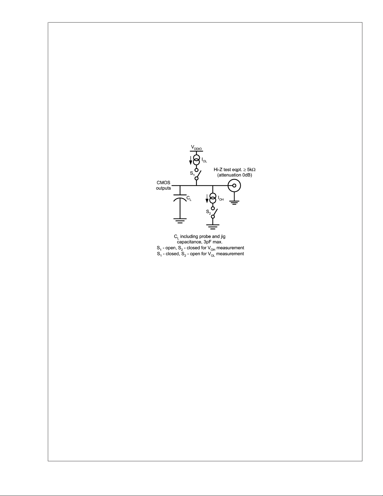
Test Loads
SSIO=VSSD
=
20020104
www.national.com 8
Test Circuit
CLC031A
20020107
www.national.com9
Timing Diagram
CLC031A
20020108
Device Operation
INTRODUCTION
The CLC031A SMPTE 292M/259M Digital Video
Deserializer/Decoder is used in digital video signal origination and destination equipment: cameras, video tape recorders, telecines, editors, standards converters, video test and
other equipment. It decodes and converts serial SDTV or
HDTV component digital video signals into parallel format.
The CLC031A decoder/deserializer processes serial digital
video (SDV) signals conforming to SMPTE 259M, SMPTE
344M (proposed) or SMPTE 292M and operates at serial
data rates of 270 Mbps, 360 Mbps, 540 Mbps, 1.483 Gbps
and 1.485 Gbps. Corresponding parallel output data rates
are 27.0 MHz, 36.0 MHz, 54.0 MHz, 74.176MHz and
74.25 MHz.
The CLC031A accepts ECL or LVDS serial data input sig-
nals. Outputs signals are compatible with LVCMOS logic
devices.
Note: In the following explanations, these logical equivalences are observed: ON
≡
and OFF
Disabled≡Reset≡False≡Logic_0.
≡
Enabled≡Set≡True≡Logic_1
VIDEO DATA PATH
The Serial Data Inputs (SDI) accept serial video data at
SMPTE 259M standard definition, SMPTE 344M (proposed)
or SMPTE 292M high-definition data rates. These inputs
accept standard ECL or LVDS signal levels and may be used
single-ended or differentially. Inputs may be DC or AC
coupled, as required, to devices and circuits supplying the
data. Recommended operating conditions and all input DC
and AC voltage and current specifications shall be observed
when designing the input coupling circuits.
For convenience, a reference bias source, pin name R
REF
sets the reference current available from the input bias
source, pin name R
is 4.75kΩ, 1%. RBBis provided so that the SDI inputs
R
REF
. The recommended nominal value of
BB
may be supplied DC bias voltage via external resistors when
the inputs are AC-coupled. The bias source should be
loaded with a resistance to the V
current available at R
input biasing scheme using R
is 200µA. Figure 1 shows a typical
BB
BB
supply. The source
SS
and R
REF
.
,
www.national.com 10

Device Operation (Continued)
20020106
FIGURE 1. Optional Input Biasing Scheme
The SMPTE descrambler receives NRZI serial data, converts it to NRZ, then decodes it to either 10-bit standard
definition or 20-bit high definition parallel video data using
the reverse polynomial X
respective standard: SMPTE 259M, SMPTE 344M (proposed) or SMPTE 292M. The data reception bit order is
LSB-first. All data processing is done at the parallel rate.
The CLC031A incorporates circuitry that implements a
method for handling data that has been subjected to LSB
dithering. When so enabled, data from the de-scrambler is
routed for de-dithering. The De-Dither Enable bit in the
VIDEO INFO 0 control register enables this function. Dedithering of data present in the vertical blanking interval can
be selectively enabled by use of the V De-Dither Enable bit
in the VIDEO INFO 0 control register. The initial condition of
De-Dither Enable and V De-Dither Enable is OFF.
The descrambler supplies signals to theTRS character de-
tector which identifies the presence of the valid video data.
The TRS character detector processes the timing reference signals which control raster framing. TRS (sync) characters are detected and the video is aligned on word boundaries. Data is re-synchronized with the parallel word-rate
9
+X4+ 1 as specified in the
clock. Interraction and operation of the character alignment
control signals and indicators Framing Mode, Framing En-
able and NSP (New Sync Position) is described later in this
datasheet.
The CLC031A implements TRS character LSB-clipping as
prescribed in ITU-R BT.601. LSB-clipping causes all TRS
characters with a value between 000h and 003h to be forced
to 000h and all TRS characters with a value between 3FCh
and 3FFh to be forced to 3FFh. Clipping is done after descrambling and de-dithering.
Once the PLL attains lock, the video format detector processes the received data to determine the raster characteristics (video data format) and configure the CLC031A to
handle it. This assures that the parallel output data will be
properly formatted, that the correct data rate is selected and
that Ancillary Data and CRC/EDH data are correctly detected and checked. Supported parallel data formats or subformats may belong to any one of several component standards: SMPTE 125M, SMPTE 267M, SMPTE 260M, 274M,
295M or 296M. Refer to Table 4 for the supported formats.
(See also the Section Application Information section for
handling of other raster formats or format extensions developed after this device was designed). The detected video
standard information is passed to the device control system
and saved in the control registers from whence it may be
read by the user.
The CLC031A may be configured to operate in a single video
format by loading the appropriate FORMAT SET[4:0] control
data into the FORMAT 0 control register. Also, the CLC031A
may be configured to handle only the standard-definition
data formats by setting the SD ONLY bit or only the highdefinition data formats by setting the HD ONLY bit in the
FORMAT 0 control register. When both bits are reset, the
default condition, the part automatically detects the data rate
and range.
Aligned and de-processed parallel data passes into a
variable-depth video FIFO prior to output. Video FIFO depth
from 0 to 4 registers is set by a 3-bit word written into the
VIDEO FIFO Depth[2:0] bits in the ANC 0 control register.
The video FIFO permits adjustment of the parallel video data
output timing or delay at a parallel word rate. The occurence
of corresponding TRS indicator bits, EAV, SAV and NSP, in
the control register corresponds to the input register position
of the FIFO. This positioning permits a look-ahead function
in which the alignment status of the video data can be
determined up to four parallel clock periods prior to the
appearance of that data at the parallel data output.
The parallel video data is output on DV[19:0]. The 20-bit
parallel video data is organized so that for HDTV data, the
upper-order 10 bits DV[19:10] are luminance (luma) information and the lower 10 bits DV[9:0] are colour difference
(chroma) information. SDTV data use the lower-order 10-bits
DV[9:0] for both luma and chroma information. (The SDTV
parallel data is also duplicated on DV[19:10]). V
parallel output word rate clock signal. The frequency of V
CLK
is the
CLK
is appropriate to either the HD or SD data being processed.
Data is valid between the falling edges of a V
cycle. Data
CLK
may be clocked into external devices on the rising-edge of
. The DV[19:0] and V
V
CLK
signals are LVCMOS-
CLK
compatible.
CLC031A
www.national.com11

Device Operation (Continued)
ANCILLARY/CONTROL DATA PATH
CLC031A
The 10-bit ancillary and Control Data Port AD[9:0] serves
two functions in the CLC031A. Ancillary Data from the An-
cillary Data FIFO is output from this port after its recovery
from the video data stream. The utilization and flow of Ancillary Data from the device is managed by a system of control
bits, masks and IDs stored in the control data registers. This
port also provides read/write access to contents of the configuration and control registers. The signals RD/WR, ANC/
CTRL and A
CONTROL DATA FUNCTIONS
Control data is input to and output from the CLC031A using
the lower-order 8 bits AD[7:0] of the ancillary/Control Data
Port. This control data initializes, monitors and controls operation of the CLC031A. The upper two bits AD[9:8] of the
port function as handshaking signals with the device accessing the port. When either a control register read or write
address is being written to the port, AD[9:8] must be driven
as 00b (0XXh, where XX are AD[7:0]). When control data is
being written to the port, AD[9:8] must be driven as 11b
(3XXh, where XX are AD[7:0]). When control data is being
read from the port, the CLC031A will output AD[9:8] as 10b
(2XXh, where XX are output data AD[7:0]) and may be
ignored by the monitoring system.
Note: After either a manual or power-on reset, A
toggled three (3) times to complete initiallization of the An-
cillary and Control Data Port.
The sequence of clock and control signals for reading control
data from the ancillary/control data port is shown in Figure 2.
Control data read mode is invoked by making the ANC/
CTRL input low and the RD/WR input high. The 8-bit ad-
dress of the control register set to be accessed is input to the
port on bits AD[7:0]. To identify the data as an address,
AD[9:8] must be driven as 00b. The complete address word
will be 0XXh, where 0 is AD[9:8] and XX are AD[7:0]. The
address is captured on the rising edge of A
control data is being read from the port, the CLC031A will
output AD[9:8] as 10b (2XXh, where XX are output data
AD[7:0]) and may be ignored by the monitoring system. Data
being output from the selected register is driven by the port
immediately following the rising edge of A
address signal is removed. For optimum system timing, the
signals driving the address to the port should be removed
control data flow through the port.
CLK
CLK
must be
CLK
. When
CLK
or when the
immediately after the address is clocked into the port and
before or simultaneously with the falling edge of A
CLK
at the
end of that address cycle. Output data remains stable until
the next rising edge of A
and may be written into external
CLK
devices at any time after the removal of the address signal.
This second clock resets the port from drive to receive and
readies the port for another access cycle.
Example: Read the Full-field Flags via the AD port.
1. Set ANC/CTRL to a logic-low.
2. Set RD/WR to a logic-high.
3. Present 001h to AD[9:0] as the register address.
4. Toggle A
CLK
.
5. Release the bus driving the AD port.
6. Read the data present on the AD port. The Full-field
Flags are bits AD[4:0].
7. Toggle A
to release the AD port.
CLK
Figure 3 shows the sequence of clock and control signals for
writing control data to the ancillary/control data port. The
control data write mode is similar to the read mode. Control data write mode is invoked by making the ANC/CTRL
input low and the RD/WR input low. The 8-bit address of the
control register set to be accessed is input to the port on bits
AD[7:0]. When a control register write address is being
written to the port, AD[9:8] must be driven as 00b (0XXh,
where XX areAD[7:0]). The address is captured on the rising
edge of A
edge of A
. The address data is removed on the falling
CLK
. Next, the control data is presented to the port
CLK
bits AD[7:0] and written into the selected register on the next
rising edge of A
. When control data is being written to the
CLK
port, AD[9:8] must be driven as 11b (3XXh, where XX are
AD[7:0]). Control data written into the registers may be read
out non-destructively in most cases.
Example: Setup (without enabling) the TPG Mode via the
AD port using the 1125 line, 30 frame, 74.25MHz, interlaced
component (SMPTE 274M) colour bars as test pattern. The
TPG may be enabled after setup using the Multi-function I/O
port or by the control registers.
1. Set ANC/CTRL to a logic-low.
2. Set RD/WR to a logic-low.
3. Present 00Dh to AD[9:0] as the Test 0 register address.
4. Toggle A
CLK
.
5. Present 027h to AD[9:0] as the register data.
6. Toggle A
CLK
.
www.national.com 12

Device Operation (Continued)
FIGURE 2. Control Data Read Timing (2 read and 1 write cycle shown)
CLC031A
20020109
FIGURE 3. Control Data Write Timing
Ancillary Data Functions
The CLC031A can recover Ancillary Data from the serial
data stream. This Ancillary Data and related control characters are defined in the relevant SMPTE standards and may
reside in the horizontal and vertical blanking intervals. The
data can consist of different types of message packets including audio data. The serial Ancillary Data space must be
formatted according to SMPTE 291M. The CLC031A sup-
ports Ancillary Data in the chrominance channel (C’r/
C’b) only for high-definition operation. Ancillary Data for
standard definition follows the requirements of SMPTE
125M.
The Ancillary Data FIFO is sized to handle a maximum
length ANC data Type 1 or Type 2 packet without the ANC
Flag, 259 words. Defined in SMPTE 291M, the packet con-
20020110
sists of the Ancillary Data Flag, a 3-word Data ID and Data
Count, 255 8- or 10-bit User Data Words and a Checksum.
The design of the CLC031A Ancillary Data FIFO also allows
storage of up to 8 shorter length messages with total length
not exceeding 259 words including all ID information. Ancil-
lary Data is copied from the data stream into the Ancillary
Data FIFO. The parallel Ancillary Data will still be present in
the parallel chroma output DV[9:0]. ancillary flag information
is not extracted into the FIFO.
Copying of ANC data from the video data into the FIFO is
controlled by the ANC Mask and ANC ID bits in the control
registers. A system of flags, ANC FIFO Empty, ANC FIFO
90% Full, ANC FIFO Full and ANC FIFO Overrun are used
to monitor FIFO status. The details and functions of these
and other control words are explained later in this datasheet.
www.national.com13

Device Operation (Continued)
Figure 4 shows the relationship of clock, data and control
CLC031A
signals for reading Ancillary Data from the port AD[9:0].In
Ancillary Data read mode, 10-bit Ancillary Data is routed
from the Ancillary Data FIFO and read from the port
AD[9:0] at a rate determined by A
Ancillary Data read (output) mode is invoked by making the
ANC/CTRL input high and the RD/WR input high. Ancillary
Data is clocked from the FIFO on the L-H transition of A
Data may be read from the port on rising edges of A
after the specified propagation delay, until the FIFO is emp-
.
CLK
FIGURE 4. Ancillary Data Read Timing
CLK
CLK
tied. Data may only be read from the port when in the
Ancillary Data mode. Ancillary Data cannot be written to the
port.
To conserve power when the Ancillary Data function is not
being used, the internal Ancillary Data FIFO clock is disabled. This clock must be enabled before Ancillary Data may
be replicated into the FIFO for output. This internal FIFO
clock is controlled by FIFO CLOCK ENABLE, bit-6 of the
ANC 5 register (address 17h). The default condition of FIFO
.
,
CLOCK ENABLE is OFF. After enabling the internal FIFO
clock by turning this bit ON, A
must be toggled three (3)
CLK
times to propagate the enable to the clock tree.
20020111
MULTI-FUNCTION I/O PORT
The multi-function I/O port can be configured to provide
immediate access to many control and indicator functions
that are stored within the CLC031A’s configuration and control registers. The individual pins comprising this port are
assigned as input or output for selected functions stored in
the control data registers.
The multi-function I/O port is configured by way of an 8x6-bit
register bank consisting of registers I/O pin 0 CONFIG
through I/O pin 7 CONFIG. The contents of these registers
determine whether the port bits function as inputs or outputs
and to which control function or indicator each port bit is
assigned. Port bits may be assigned to access different
functions and indicators or any or all port bits may be assigned to access the same function or indicator (output
mode only). The same indicator or function should not be
assigned to more than one port bit as an input. Controls and
indicators that are accessible by the port and their corresponding selection addresses are given in the I/O Pin Configuration Register Addresses, Table 6. Table 2 gives the
control register bit assignments.
Data resulting from device operation will be sent to the
selected I/O port bit. This same data is also stored in the
configuration and control registers. Mapping the control and
indicator functions in this manner means that device operation will be immediately reflected at the I/O port pins thereby
ensuring more reliable real-time operation of the device
within and by the host system.
When a multifunction I/O port bit is used as input to a control
register bit, data must be presented to the I/O port bit and
clocked into the register bit using A
as shown in Figure 5.
CLK
Port timing for bit write operations is the same as for the
ANC/CTRL port operation.
20020112
FIGURE 5. I/O Port Data Write Timing
Example: Program multi-function I/O port bit-0 as the CRC
Luma Error bit output.
1. Set ANC/CTRL to a logic-low.
2. Set RD/WR to a logic-low.
3. Present 00Fh to AD[9:0] as the I/O PIN 0 CONFIG
register address.
4. Toggle A
CLK
.
5. Present 310h to AD[9:0] as the register data.
6. Toggle A
CLK
.
EDH/CRC SYSTEM The CLC031A has EDH and CRC character generation
and checking circuitry. The EDH system functions as de-
scribed in SMPTE Recommended Practice RP-165. The
CRC system functions as specified in SMPTE 292M. The
EDH/CRC polynomial generators/checkers accept parallel data from the de-serializing system and generate the
EDH and CRC check words for comparison with those received in the data.
The EDH Enable bit in the control register enables the EDH
generation and checking system. Incoming SDTV data is
checked for errors and the EDH flags are updated automati-
www.national.com 14

Device Operation (Continued)
cally. EDH errors are reported in the EDH0, EDH1, and
EDH2 register sets of the configuration and control registers.
Updated or new EDH check words and flags may be generated and inserted in the data. EDH check words are generated using the polynomial X
RP165. Generation and automatic insertion of new or corrected EDH check words is controlled by EDH Force and
EDH Enable bits in the control registers. EDH check words
and status flags are inserted in the parallel data at the
correct positions in the Ancillary Data space and formatted
per SMPTE 291M. After a reset, the initial state of all EDH
and CRC check characters is 00h.
The SMPTE 292M high definition video standard employs
CRC (cyclic redundancy check codes) error checking instead of EDH. The CRC consists of two 18-bit words generated using the polynomial X
292M. One CRC is used for luminance and one for chrominance data. The CRCs appear in the data stream following
the EAV and line number characters. The CRCs are checked
and errors are reported in the EDH0, EDH1, and EDH2
register sets of the configuration and control registers.
PHASE-LOCKED LOOP / CLOCK-DATA RECOVERY SYSTEM
The phase-locked loop and clock-data recovery (PLL/
CDR) system generates all internal timing and data rate
clocks for the CLC031A. The PLL/CDR system consists of
five main functional blocks: 1) the input buffer which receives
the incoming data, 2) input data samplers which oversample
the data coming from the input buffer, 3) a PLL (VCO, divider
chain, phase-frequency detector and internal loop filter)
which generates sampling and other system clocks, 4) a
digital CDR system to recover the oversampled serial input
data from the samplers and the digital system control and 5)
a rate detect controller which sequences the PLL to find the
data rate.
Using an oversampling technique, the timing information
encoded in the serial data is extracted and used to synchronize the recovered clock and data. The parallel data rate and
other clock signals are derived from the regenerated serial
clock. The parallel data rate clock is 1/10th of the serial data
rate clock for standard definition or 1/20th of the serial data
clock frequency for high definition. The data interface between the CDR and the digital processing block uses 10-bit
data plus the required clocks.
The PLL is held in coarse frequency lock by an external
27MHz clock signal, EXT CLK, or by an external 27MHz
crystal and internal oscillator. Upon power-on, EXT CLK is
the default reference. The internal oscillator and an external
crystal may be used as the reference by setting the OSCEN
bit in the CDR register. The reference clock reduces lock
latency and enhances format and auto-rate detection robust-
16+X12+X6
18+X5+X4
+ 1 per SMPTE
+ 1 per SMPTE
ness. PLL acquisition, data phase alignment and format
detection time is 20ms or less at 1.485Mbps. The VCO has
separate V
DDPLL
and V
power supply feeds, pins 51
SSPLL
and 52, which may be supplied power via an external lowpass filter, if desired.
20020105
FIGURE 6. Crystal and Load Circuit
A 27MHz crystal and load circuit may be used to provide the
reference clock. A fundamental mode crystal with the following parameters is used: frequency 27MHz, frequency toler-
±
30ppm, load capacitance 18pF, maximum drive level
ance
100µW, equivalent series resistance
<
50Ω, operating temperature range 0˚C to 70˚C. Refer to Figure 6 for a typical
load circuit and connection information.
The CLC031A indicates that the PLL is locked to the incoming data rate and that the CDR has acquired a phase of the
serial data by setting the Lock Detect bit in the Video Info 0
control register. Indication of the standard being processed
is retained in the FORMAT[4:0] bits in the FORMAT 1 control data register. Format data from this register can be
programmed for output on the multi-function I/O port. The
power-on default assigns Lock Detect as I/O Port bit 4.
POWER SUPPLIES, POWER-ON-RESET AND RESET INPUT
The CLC031A requires two power supplies, 2.5V for the core
logic functions and 3.3V for the I/O functions. The supplies
must be applied to the device in proper sequence. The 3.3V
supply must be applied prior to or coincident with the 2.5V
supply. Application of the 2.5V supply must not precede the
3.3V supply. It is recommended that the 3.3V supply be
configured or designed so as to control application of the
2.5V supply in order to satisfy this sequencing requirement.
The CLC031A has an automatic, power-on-reset circuit.
Reset initializes the device and clears TRS detection circuitry, all latches, registers, counters and polynomial
generators/checkers and resets the EDH/CRC characters to
00h. An active-HIGH-true, manual reset input is available at
pin 49. The reset input has an internal pull-down device and
may be considered inactive when unconnected.
Important: When power is first applied to the device or
following a reset, the ancillary and Control Data Port must
be initialized to receive data. This is done by toggling A
CLK
three times.
CLC031A
www.national.com15

Device Operation (Continued)
TEST PATTERN GENERATOR (TPG) AND BUILT-IN
CLC031A
SELF-TEST (BIST)
The CLC031A includes an on-board, parallel video test pat-
tern generator (TPG). Four test pattern types are available
in both HD and SD formats, NTSC and PAL standards, and
4x3 and 16x9 raster sizes. The test patterns are: flat-field
black, PLL pathological, equalizer (EQ) pathological and a
75%, 8-colour vertical bar pattern. The pathologicals follow
recommendations contained in SMPTE RP 178-1996 regarding the test data used. The colour bar pattern has optional bandwidth limiting coding in the chroma and luma data
transitions between bars. The VPG FILTER ENABLE bit in
the VIDEO INFO 0 control register enables the colour bar
filter function. The test pattern data is available at the video
data outputs, DV[19:0] with a corresponding parallel rate
clock, VCLK, appropriate to the particular standard and
format selected.
The TPG also functions as a built-in self-test (BIST) which
can be used to verify device functionality. The BIST function
performs a comprehensive go/no-go test of the device. The
test may be run using any of the HD colour bar patterns or
one of two SD patterns, either the 270 Mb/s NTSC colour bar
or the PAL PLL pathological, as the test data pattern. Data is
input from the digital processing block, processed through
the device and tested for errors using either the EDH system
for SD or the CRC system for HD. Clock signals from the
CDR block supply timing for the test data. The CDR must be
supplied a 27MHz reference clock via the XTALi/Ext Clk
input (or using the internal oscillator and crystal) during the
TPG or BIST function. A go/no-go indication is logged in the
Pass/Fail bit of the TEST 0 control register set. This bit may
be assigned as an output on the multifunction I/O port.
TPG and BIST operation is initiated by loading the code for
the desired test pattern into the Test Pattern Select[5:0] bits
and by setting the TPG Enable bit of the TEST 0 register.
Note that when attempting to use the TPG or BIST immediately after the device has been reset or powered on, the TPG
defaults to the 270Mbps SD rate. The device must be configured for the desired test pattern by loading the appropriate
code in to the TEST 0 register. If HD operation is desired,
selection of the desired HD test pattern is sufficient to enable
the device to configure itself to run at the correct rate and
generate valid data. Table 5 gives the available test patterns
and codes.
The Pass/Fail bit in the control register gives the device test
status indication. If no errors have been detected, this bit will
be set to logic-1 approximately 2 field intervals after TPG
Enable is set. If errors have been detected in the internal
circuitry of the CLC031A, Pass/Fail will remain reset to a
logic-0. TPG or BIST operation is stopped by resetting the
TPG Enable bit. Parallel output data is present at the
DV[19:0] outputs during TPG or BIST operation.
Example: Enable the TPG Mode to use the NTSC 270Mbps
colour bars as the BIST and TPG pattern. Enable TPG
operation using the I/O port.
1. Set ANC/CTRL to a logic-low.
2. Set RD/WR to a logic-low.
3. Present 00Dh to AD[9:0] as the TEST 0 register address.
4. Toggle A
CLK
.
5. Present 343h to AD[9:0] as the register data (525 line,
30 frame, 27MHz, NTSC 4x3, colour bars (SMPTE
125M)).
6. Toggle A
CLK
.
7. The PASS/FAIL indicator, TEST 0 register, Bit 7, should
be read for the result of the test. Alternatively, this bit
may be mapped to a convenient bit of the Multi-function
I/O bus. The test pattern data and clock is available at
the DV[19:0] and V
CLK
outputs.
CONFIGURATION AND CONTROL REGISTERS
The configuration and control registers store data which
determines the operational modes of the CLC031A or which
result from its operation. Many of these registers may be
assigned as external I/O functions which are then available
on the multi-function I/O bus. These functions are summarized in Table 1 and detailed in Table 2. The power-on default
condition for the multi-function I/O port is indicated in Table 1
and detailed in Table 6.
www.national.com 16

Device Operation (Continued)
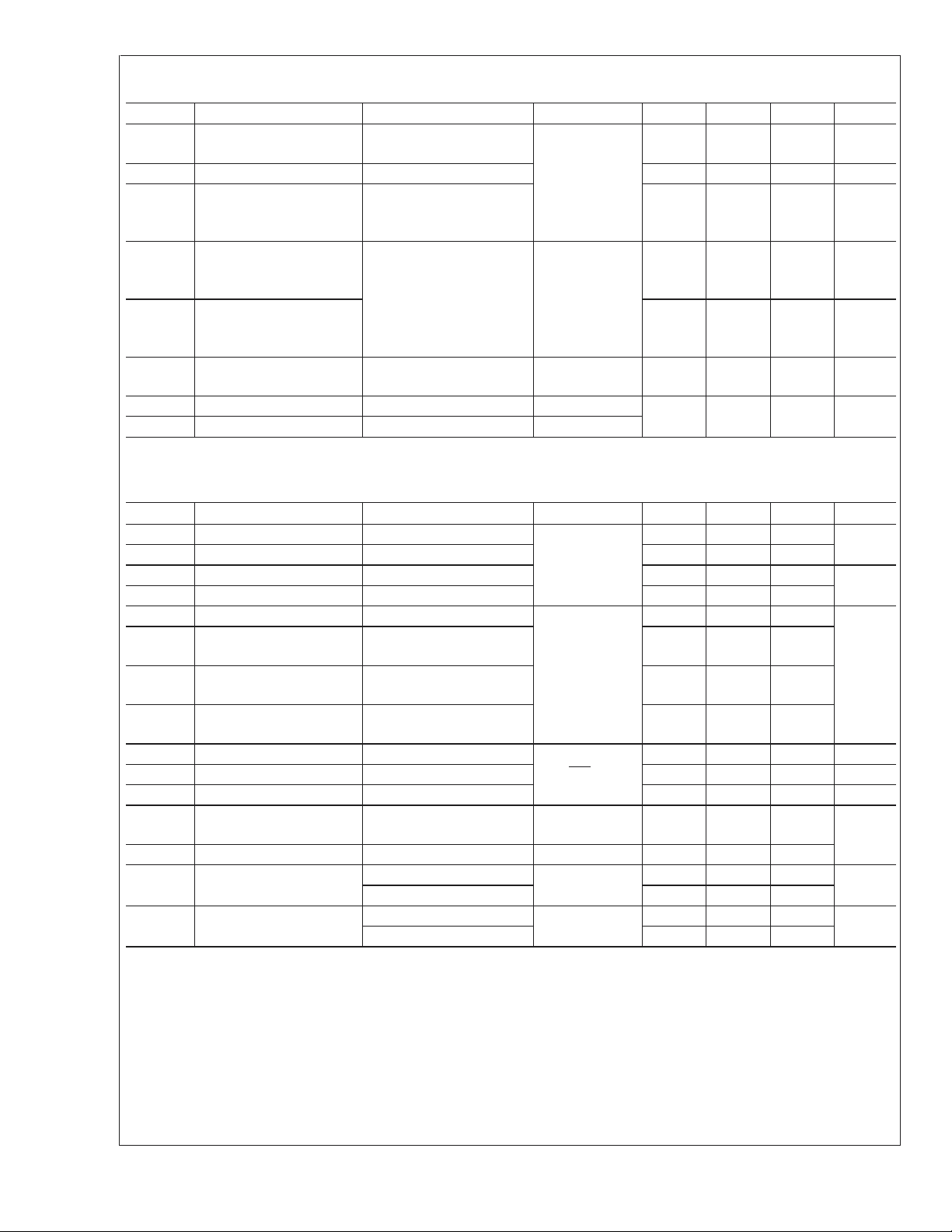
TABLE 1. Configuration and Control Data Register Summary
Register Function Bits Read or Write Initial Condition
EDH and CRC Operations
CRC Error (SD/HD) 1 R Reset Output (Note 11) I/O 5
CRC Error Luma 1 R Reset Output
CRC Error Chroma 1 R Reset Output
CRC Replace 1 R/W OFF No (Note 13)
Full-Field Flags 5 R Reset No
Active Picture Flags 5 R Reset No
ANC Flags 5 R Reset No
EDH Force 1 R/W OFF Input
EDH Enable 1 R/W ON Input
F/F Flag Error 1 R Reset Output
A/P Flag Error 1 R Reset Output
ANC Flag Error 1 R Reset Output
Ancillary Data Operations
ANC Checksum Force 1 R/W OFF Input
ANC Checksum Error 1 R Reset Output
ANC FIFO Empty 1 R Set Output (Note 11) I/O 6
ANC FIFO 90% Full 1 R Reset Output
ANC FIFO Full 1 R Reset Output
ANC FIFO Overrun 1 R Reset Output
ANC ID 16 R/W 0000h No
ANC Mask 16 R/W FFFFh No
MSG Track 1 R/W OFF No
MSG Flush Static 1 R/W OFF No
FIFO Flush Static 1 R/W OFF No
Full MSG Available 1 R OFF Output
Short MSG Detect 1 R OFF Output
FIFO Clock Enable 1 R/W OFF No
FIFO Extract Enable 1 R/W OFF Input
Video FIFO Operation
Video FIFO Depth 3 R/W 000b No
Video Format Operations
Format Set 5 R/W 00000B No
SD Only 1 R/W OFF No
HD Only 1 R/W OFF No
Format 5 R Output Format [4] (Note 11)
H 1 R Output (Note 11) I/O 2
V 1 R Output (Note 11) I/O 1
F 1 R Output (Note 11) I/O 0
Framing Mode 1 R/W ON No
Framing Enable 1 R/W ON Input
New Sync Position (NSP) 1 R Output
SAV 1 R Output
EAV 1 R Output (Note 11) I/O 7
De-scramble Enable 1 R/W ON No
NRZI Enable 1 R/W ON No
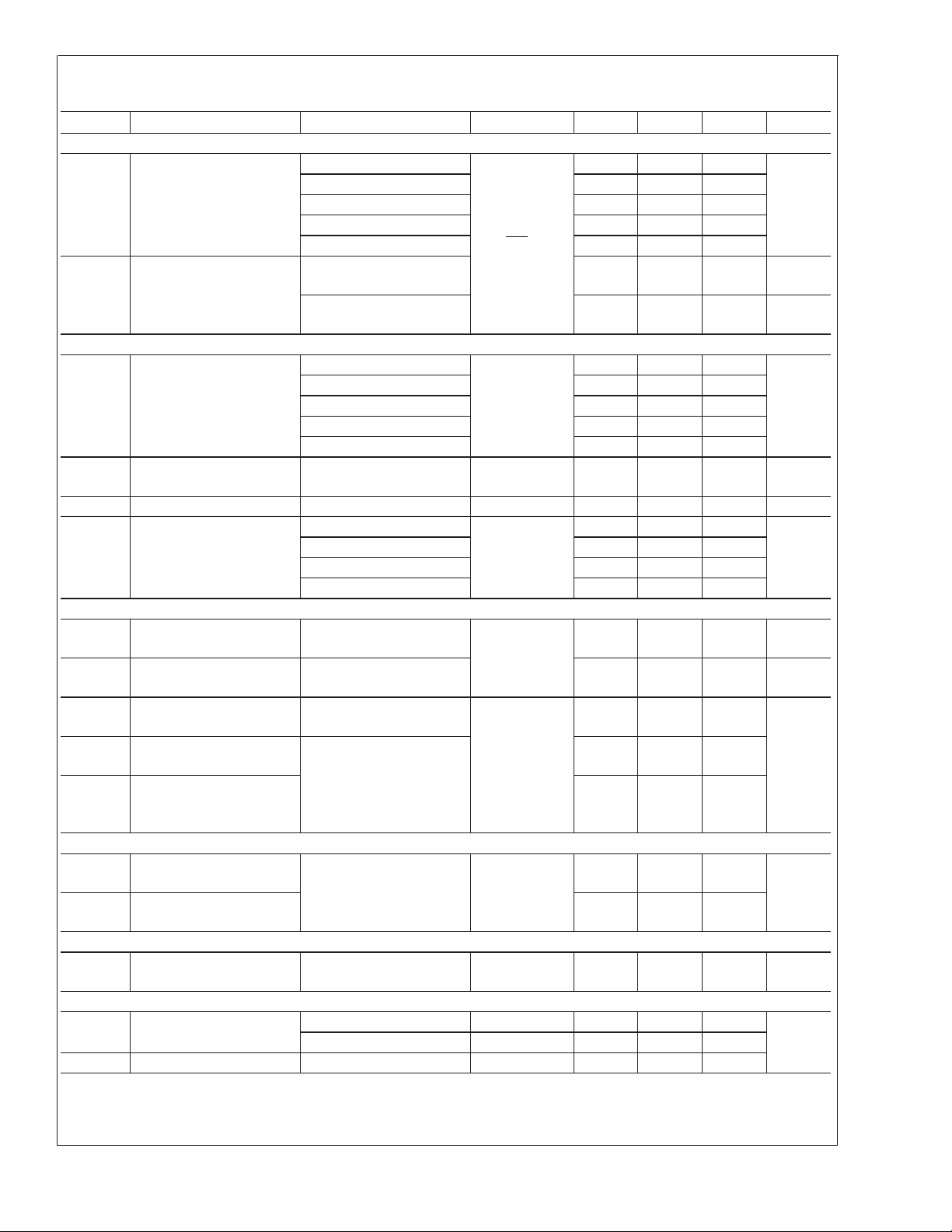
Available on
I/O Bus
Notes
I/O 3
CLC031A
www.national.com17

Device Operation (Continued)
CLC031A
Register Function Bits Read or Write Initial Condition
LSB Clipping Enable 1 R/W ON No
Sync Detect Enable 1 R/W ON No
De-Dither Enable 1 R/W OFF Input
Vert. De-Dither Enable 1 R/W OFF Input
Lock Detect 1 R Output (Note 11) I/O 4
Unscrambled
Video Data Out
TPG and BIST Operations
Test Pattern Select 6 R/W 000000b Input 525/27 MHz/Black
TPG Enable 1 R/W OFF Input
Pass/Fail 1 R Output
VPG Filter Enable 1 R/W OFF Input
Reference Clock Operations
Reference Clock 2 R/W 00b No EXT CLK Enabled
External Vclk 1 R/W OFF No (Note 13)
Multifunction I/O Bus Operations
I/O Bus Pin Config. 48 R/W See Table 6 No
Note 11: Connected to multifunction I/O port at power-on.
Note 12: ON = SET = logic-1, OFF = RESET = logic-0 (positive logic).
Note 13: Special or restricted functionality. Refer to text for details.
TABLE 1. Configuration and Control Data Register Summary (Continued)
Available on
I/O Bus
1 R/W OFF No (Note 13)
Notes
TABLE 2. Control Register Bit Assignments
Bit 7 Bit 6 Bit 5 Bit 4 Bit 3 Bit 2 Bit 1 Bit 0
EDH 0 (register address 01h)
CRC ERROR EDH FORCE EDH ENABLE F/F UES F/F IDA F/F IDH F/F EDA F/F EDH
EDH 1 (register address 02h)
CRC
REPLACE
EDH 2 (register address 03h)
F/F FLAG
ERROR
ANC 0 (register address 04h)
VIDEO
FIFO-DEPTH(2)
ANC 1 (register address 05h)
ANC ID(7) ANC ID(6) ANC ID(5) ANC ID(4) ANC ID(3) ANC ID(2) ANC ID(1) ANC ID(0)
ANC 2 (register address 06h)
ANC ID(15) ANC ID(14) ANC ID(13) ANC ID(12) ANC ID(11) ANC ID(10) ANC ID(9) ANC ID(8)
ANC 3 (register address 07h)
ANC MASK(7) ANC MASK(6) ANC MASK(5)
ANC 4 (register address 08h)
ANC
MASK(15)
ANC 5 (register address 17h)
FIFO
EXTRACT
ENABLE
CRC ERROR
LUMA
A/P FLAG
ERROR
VIDEO
FIFO-DEPTH(1)
ANC MASK(14) ANC MASK(13)
FIFO CLOCK
ENABLE
CRC ERROR
CHROMA
ANC FLAG
ERROR
VIDEO
FIFO-DEPTH(0)
FULL MSG
AVAILABLE
A/P UES A/P IDA A/P IDH A/P EDA A/P EDH
ANC UES ANC IDA ANC IDH ANC EDA ANC EDH
ANC FIFO
OVERRUN
ANC
MASK(4)
ANC
MASK(12)
reserved
ANC FIFO
EMPTY
ANC
MASK(3)
ANC
MASK(11)
FIFO FLUSH
STATIC
ANC FIFO
FULL
ANC
MASK(2)
ANC
MASK(10)
reserved
ANC CHECKSUM ERROR
ANC
MASK(1)
ANC
MASK(9)
MSG FLUSH
STATIC
ANC CHECK-
SUM FORCE
ANC
MASK(0)
ANC
MASK(8)
MSG TRACK
www.national.com 18

Device Operation (Continued)
TABLE 2. Control Register Bit Assignments (Continued)
Bit 7 Bit 6 Bit 5 Bit 4 Bit 3 Bit 2 Bit 1 Bit 0
ANC 6 (register address 18h)
ANC FIFO
90% FULL
FORMAT 0 (register address 0Bh)
FRAMING
MODE
FORMAT 1 (register address 0Ch)
F V H FORMAT(4) FORMAT(3) FORMAT(2) FORMAT(1) FORMAT(0)
TEST 0 (register address 0Dh)
PASS/FAIL TPG ENABLE
VIDEO INFO 0 (register address 0Eh)
DE-DITHER
ENABLE
VIDEO CONTROL 0 (register address 55h)
reserved
REFERENCE CLOCK (register address 67h)
reserved reserved reserved reserved reserved INT_OSC EN CLK EN
MULTI-FUNCTION I/O BUS PIN CONFIGURATION
I/O PIN 0 CONFIG (register address 0Fh)
reserved reserved PIN 0 SEL[5] PIN 0 SEL[4] PIN 0 SEL[3] PIN 0 SEL[2] PIN 0 SEL[1] PIN 0 SEL[0]
I/O PIN 1 CONFIG (register address 10h)
reserved reserved PIN 1 SEL[5] PIN 1 SEL[4] PIN 1 SEL[3] PIN 1 SEL[2] PIN 1 SEL[1] PIN 1 SEL[0]
I/O PIN 2 CONFIG (register address 11h)
reserved reserved PIN 2 SEL[5] PIN 2 SEL[4] PIN 2 SEL[3] PIN 2 SEL[2] PIN 2 SEL[1] PIN 2 SEL[0]
I/O PIN 3 CONFIG (register address 12h)
reserved reserved PIN 3 SEL[5] PIN 3 SEL[4] PIN 3 SEL[3] PIN 3 SEL[2] PIN 3 SEL[1] PIN 3 SEL[0]
I/O PIN 4 CONFIG (register address 13h)
reserved reserved PIN 4 SEL[5] PIN 4 SEL[4] PIN 4 SEL[3] PIN 4 SEL[2] PIN 4 SEL[1] PIN 4 SEL[0]
I/P PIN 5 CONFIG (register address 14h)
reserved reserved PIN 5 SEL[5] PIN 5 SEL[4] PIN 5 SEL[3] PIN 5 SEL[2] PIN 5 SEL[1] PIN 5 SEL[0]
I/O PIN 6 CONFIG (register address 15h)
reserved reserved PIN 6 SEL[5] PIN 6 SEL[4] PIN 6 SEL[3] PIN 6 SEL[2] PIN 6 SEL[1] PIN 6 SEL[0]
I/O PIN 7 CONFIG (register address 16h)
reserved reserved PIN 7 SEL[5] PIN 7 SEL[4] PIN 7 SEL[3] PIN 7 SEL[2] PIN 7 SEL[1] PIN 7 SEL[0]
SHORT MSG
DETECT
SD ONLY HD ONLY
VERT.
DE-DITHER
ENABLE
EXTERNAL
V
CLK
ANC PARITY
MASK
TEST
PATTERN
SELECT(5)
VPG FILTER
ENABLE
SYNC DETECT
ENABLE
reserved reserved reserved reserved VANC
FORMAT
SET(4)
TEST
PATTERN
SELECT(4)
LOCK
DETECT
LSB CLIP
ENABLE
FORMAT
SET(3)
TEST
PATTERN
SELECT(3)
EAV SAV NSP
reserved
FORMAT
SET(2)
TEST
PATTERN
SELECT(2)
NRZI
ENABLE
FORMAT
SET(1)
TEST
PATTERN
SELECT(1)
DE-Scramble
ENABLE
FORMAT
SET(0)
TEST
PATTERN
SELECT(0)
FRAMING
ENABLE
reserved
reserved
CLC031A
www.national.com19

Device Operation (Continued)
CLC031A
EDH 0 (register 01h)
The EDH Full-Field flags F/F UES, F/F IDA, F/F IDH, F/F
EDA andF/F EDH are defined in SMPTE RP 165. The flags
are updated automatically when the EDH function is enabled
and data is being received.
The EDH ENABLE bit, when set, enables operation of the
EDH generator function during SD operation. The default
condition of this bit is set (ON).
The EDH FORCE bit, when set, causes updated EDH packets to be inserted in the parallel output data regardless of the
previous condition of EDH checkwords and flags in the input
serial data. This function may be used in situations where
video content has been edited thus making the previous
EDH information invalid. The default condition of this bit is
reset (OFF).
The CRC ERROR bit indicates that errors in either the EDH
checksums (SD) or CRC checkwords (HD) were detected in
the serial input data. This bit is a combined function which
indicates the presence of either EDH errors during SD operation or CRC errors during HD operation.
EDH 1 (register 02h)
The EDH Active Picture flags A/P UES, A/P IDA, A/P IDH,
A/P EDA andA/P EDH are defined in SMPTE RP 165. The
flags are updated automatically when the EDH function is
enabled and data is being received.
TABLE 3. Control Register Addresses
Register Name
EDH 0 01
EDH 1 02
EDH 2 03
ANC 0 04
ANC 1 05
ANC 2 06
ANC 3 07
ANC 4 08
ANC 5 17
ANC 6 18
FORMAT 0 0B
FORMAT 1 0C
TEST 0 0D
VIDEO INFO 0 0E
I/O PIN 0 CONFIG 0F
I/O PIN 1 CONFIG 10
I/O PIN 2 CONFIG 11
I/O PIN 3 CONFIG 12
I/O PIN 4 CONFIG 13
I/O PIN 5 CONFIG 14
I/O PIN 6 CONFIG 15
I/O PIN 7 CONFIG 16
VIDEO CONTROL 0 55
VIDEO CONTROL 1 56
REFERENCE CLOCK 67
Address
Hexadecimal
Specific types of CRC errors in incoming HD serial data are
reported in the CRC ERROR LUMA and CRC ERROR
CHROMA bits.
The CRC REPLACE bit, when set, causes the CRCs in the
incoming data to be replaced with CRCs calculated by the
CLC031A. The bit is normally reset (OFF).
EDH 2 (register 03h)
The EDH Ancillary Data flags ANC UES, ANC IDA, ANC
IDH, ANC EDA andANC EDH are defined in SMPTE RP
165. The flags are updated automatically when the EDH
function is enabled and data is being received.
The status of EDH flag errors in incoming SD serial data are
reported in the ffFlagError, apFlagError and ancFlagError
bits. Each of these bits is the logical-OR of the corresponding EDH and EDA flags.
ANC 0 (Address 04h)
The V FIFO Depth[2:0] bits control the depth of the video
FIFO which preceeds the parallel output data drivers. The
depth can be set from 0 to 4 stages by writing the corresponding binary code into these bits. For example: to set the
Video FIFO depth at two registers, load 11010XXXXXb into
the ANC 0 control register (where X represents the other
functional bits of this register).
Note: When changing some but not all bits in a register and
to retain unchanged other data previously stored in the
register, read the register’s contents and logically-OR this
with the new data. Then write the modified data back into the
register.
Flags for ANC FIFO EMPTY, ANC FIFO 90% FULL, ANC
FIFO FULL and ANC FIFO OVERRUN are available in the
configuration and control register set. These flags can also
be assigned as outputs on the multi-function I/O port. ANC
FIFO EMPTY when set indicates that the FIFO contains no
data. ANC FIFO 90% FULL indicates when the FIFO is at
90% of capacity. Since it is virtually impossible for the host
processor to begin extracting data from the FIFO after it has
been flagged as full without the possibility of an overrun
condition occurring, ANC FIFO 90% FULL is used as an
advanced command to the host to begin extracting data from
the FIFO. To be used properly, ANC FIFO 90% FULL should
be assigned as an output on the multi-function I/O port and
monitored by the host system. Otherwise, inadvertent loss of
ancillary packet data could occur. ANC FIFO FULL when set
indicates that the FIFO registers are completely filled with
data.
The ANC FIFO OVERRUN flag indicates that an attempt to
write data into a full FIFO has occurred. ANC FIFO OVER-
RUN can be reset by reading the bit’s status via the ancillary/
Control port. If an overrun occurrs, the status of the FIFO
message tracking will be invalidated. In this event, the FIFO
should be flushed to reset the message tracking pointers.
Any messages then in the FIFO will be lost.
The ANC Checksum Force bit, under certain conditions,
enables the overwriting of Ancillary Data checksums received in the data. Calculation and insertion of new Ancillary
Data checksums is controlled by the ANC Checksum Force
bit. If a checksum error is detected (calculated and received
checksums do not match) and the ANC Checksum Force
bit is set, the ANC Checksum Error bit is set and a new
checksum is inserted in the Ancillary Data replacing the
previous one. If a checksum error is detected and the ANC
Checksum Force bit is not set, the checksum mismatch is
www.national.com 20

Device Operation (Continued)
reported via the ANC Checksum Error bit. ANC Checksum
Error is available as an output on the multifunction I/O port.
ANC 1 AND 2 (Addresses 05h and 06h)
The extraction of Ancillary Data packets from video data into
the FIFO is controlled by the ANC MASK[15:0] and ANC
ID[15:0] bits in the control registers. The ANC ID[7:0] register normally is set to a valid 8-bit code used for component
Ancillary Data packet DID identification as specified in
SMPTE 291M-1998. Similarly, ANC ID[15:8] normally is set
to a valid 8-bit code used for component Ancillary Data
packet SDID/DBN identification.
ANC 3 AND 4 (Addresses 07h and 08h)
The ANC MASK[7:0] is an 8-bit word that can be used to
selectively control extraction of packets with specific DIDs
(or DID ranges) into the FIFO. When the ANC MASK[7:0] is
set to FFh, packets with any DID can be extracted into the
FIFO. When any bit or bits of the ANC MASK[7:0] are set to
a logic-1, the corresponding bit or bits of the ANC ID[7:0] are
a don’t-care when matching DIDs of packets being extracted. When the ANC MASK[7:0] is set to 00h, the ANC
DID of incoming packets must match exactly, bit-for-bit the
ANC ID[7:0] set in the control register for the packets to be
extracted into the FIFO. The initial value of the ANC
MASK[7:0] is FFh and the ANC ID[7:0] is 00h.
Similarly, ANC MASK[15:8] is an 8-bit word that can be
used to selectively control extraction of packets with specific
SDID/DBN (or SDID/DBN ranges) into the FIFO. Operation
and use of these bits is the same as for ANC MASK[7:0]
previously discussed.
ANC 5 (Address 17h)
The FIFO EXTRACT ENABLE bit in the control registers
enables the device to extract or copy Ancillary Data from the
video data stream and place it in the ANC FIFO. From there
data may be output via the parallel ancillary port. Data
extraction is enabled when this bit is set to a logic-1. This bit
can be used to delay automatic extraction and therefore the
output of parallel Ancillary Data. FIFO EXTRACT ENABLE
should be asserted during an SAV or EAV to avoid timing
problems with Ancillary Data extraction. Access to data in the
FIFO is controlled by the RD/WR, ANC/CTRL and A
control signals.
To conserve power when the Ancillary Data function is not
being used, the internal Ancillary Data FIFO clock is disabled. This clock must be enabled before Ancillary Data may
be replicated into the FIFO for output. FIFO CLOCK EN-
ABLE, bit-6 of the ANC 5 register (address 17h), when set,
enables this clock to propagate to the FIFO. The default
condition of FIFO CLOCK ENABLE is OFF. After enabling
the internal FIFO clock by turning this bit ON, A
CLK
toggled three (3) times to propagate the enable to the clock
tree. A
should remain running at all times when the ANC
CLK
FIFO is in use. Otherwise, message tracking and related
functions will not operate correctly.
The CLC031A can keep track of up to 8 ANC data packets in
the ANC FIFO. Incoming packet length versus available
space in the FIFO is also tracked. The MSG TRACK bit in
the control registers, when set, enables tracking of packets
in the FIFO. Other functions for control of packet traffic in the
CLK
must be
CLC031A
FIFO are FIFO FLUSH STAT and MSG FLUSH STAT.Ifthe
user wishes to handle more than 8 messages, the MSG
TRACK bit should be turned off (reset). The operation FIFO
FLUSH STAT will no longer work and the function FULL
MSG AVAILABLE will no longer be a reliable indicator that
messages are available in the FIFO. The user may still
effectively use the FIFO by monitoring the states of ANC
FIFO EMPTY, ANC FIFO FULL, ANC FIFO 90%FULL and
ANC FIFO OVERRUN.
Setting the FIFO FLUSH STAT bit to a logic-1 flushes the
FIFO. FIFO FLUSH STAT may not be set while the FIFO is
being accessed (Read or Write). FIFO FLUSH STAT is
automatically reset after this operation is complete.
When MSG FLUSH STAT is set to a logic-1, the oldest
message packet in the FIFO is flushed when data is not
being written to the FIFO. MSG FLUSH STAT is automati-
cally reset after this operation is complete.
The FULL MSG AVAILABLE bit in the control registers,
when set, notifies the host system that complete packets
reside in the Ancillary Data FIFO. When this bit is not set, the
messages in the FIFO are incomplete or partial. This function is not affected by MSG TRACK. The FULL MSG AVAIL-
ABLE function is most useful when mapped to the multifunction I/O port as an output.
ANC 6 (Address 18h)
The ANC FIFO 90% FULL flag bit indicates when the ANC
FIFO is 90% full. This bit may be mapped to the multifunction I/O port. The purpose of this flag is to provide a
signal which gives the host system time to begin reading
from the FIFO before it has the chance to overflow. This was
done because it is virtually impossible to monitor the FIFO
FULL flag and begin extracting from the FIFO before an
overrun condition occurs.
The SHORT MSG DETECT flag bit indicates when short
ANC messages have been detected. i.e. An ANC header
was detected before the last full message was recovered.
This bit may be mapped to the multi-function I/O port.
The ANC PARITY MASK bit when set disables parity checking for DID and SDID words in the ANC data packet. When
reset, parity checking is enabled; and, if a parity error occurs,
the packet will not be extracted.
The VANC bit, when set, enables extraction of ANC data
present in the vertical blanking interval (both active video
and horizontal blanking portions of the line).
FORMAT 0 (Address 0Bh)
The CLC031A may be set to process a single video format
by writing the appropriate data into the FORMAT 0 register.
The Format Set[4:0] bits confine the CLC031A to recognize
and process only one of the fourteen specified type of SD or
HD formats defined by a particular SMPTE specification. The
Format Set[4:0] bits may not be used to confine device
operation to a range of standards. The available formats and
codes are detailed in Table 4. Generally speaking, the For-
mat Set[4:0] codes indicate or group the formats as follows:
Format Set[4] is set for the HD data formats, reset for SD
data formats. Format Set[3] is set for PAL data formats (with
the exception of the SMPTE 274M 24-frame progressive
format), reset for NTSC data formats. Format Set[2:0] further sub-divide the standards as given in the table.
www.national.com21

Device Operation (Continued)
CLC031A
Format
Code
[4,3,2,1,0]
00001 SDTV, 54 RP 174 60I 525 507/487* 3432 2880
00010 SDTV, 36 SMPTE 267 60I 525 507/487* 2288 1920
00011 SDTV, 27 SMPTE 125 60I 525 507/487* 1716 1440
01001 SDTV, 54 ITU-R BT 601.5 50I 625 577 3456 2880
01010 SDTV, 36 ITU-R BT 601.5 50I 625 577 2304 1920
01011 SDTV, 27 ITU-R BT 601.5 50I 625 577 1728 1440
10001 HDTV, 74.25 SMPTE 260 30I 1125 1035 2200 1920
10010 HDTV, 74.25 SMPTE 274 30I 1125 1080 2200 1920
10011 HDTV, 74.25 SMPTE 274 30P 1125 1080 2200 1920
11001 HDTV, 74.25 SMPTE 274 25I 1125 1080 2640 1920
11010 HDTV, 74.25 SMPTE 274 25P 1125 1080 2640 1920
11100 HDTV, 74.25 SMPTE 295 25I 1250 1080 2376 1920
11101 HDTV, 74.25 SMPTE 274 24P 1125 1080 2750 1920
10100 HDTV, 74.25 SMPTE 296 (1, 2) 60P 750 720 1650 1280
The HD Only bit when set to a logic-1 locks the CLC031A
into the high definition data range and frequency. In systems
designed to handle only high definition signals, enabling HD
Only reduces the time required for the CLC031A to establish
frequency lock and determine the HD format being processed.
The SD Only bit when set to a logic-1 locks the CLC031A
into the standard definition data ranges and frequencies. In
systems designed to handle only standard definition signals,
enabling SD Only reduces the time required for the
CLC031A to establish frequency lock and determine the
format being processed. When SD Only and HD Only are
set to logic-0, the device operates in SD/HD mode.
The Framing Mode bit in the Format 0 register and Fram-
ing Enable in the Video Info 0 register combine with Framing Enable to control the manner in which the CLC031A
aligns framing. When Framing Mode and Framing Enable
are both reset, the CLC031A aligns on the first valid TRS
character. If another TRS occurs that is not on a word
boundary, the NSP bit is set until the next TRS that is on a
word boundary occurs. When Framing Mode is set to a
logic-1, the CLC031A operates similarly to the CLC011 when
NSP is tied to FE. An alternative configuration that operates
identically can be achieved with the CLC031A by mapping
NSP as an output and Framing Enable as an input on the
Multifunction I/O bus and externally connecting them. In this
case Framing Mode should be reset to a logic-0. When
Framing Mode is reset and Framing Enable is set, the
CLC031A realigns on every valid TRS. The initial state of
Framing Mode is set following a reset or at power-on.
FORMAT 1 (Address 0Ch)
The CLC031A automatically determines the format of the
incoming serial data. The result of this operation is stored in
the FORMAT 1 register. The Format[4:0] bits identify which
Format Spec.
TABLE 4. Video Raster Format Parameters
Frame
Rate
Lines Active Lines Samples
of the many possible video data standards that the CLC031A
can process is being received. These format codes follow
the same arrangement as for the Format Set[4:0] bits.
These formats and codes are given in Table 4. Bit Format[4]
when set indicates that HD data is being processed. When
reset, SD data is indicated. Format[3] when set indicates
that PAL data is being processed. When reset NTSC data is
being processed. Format[2:0] correspond with one of the
sub-standards given in the table. Note that the CLC031A
does not distinguish or log the data rate differences between
HD data at 74.25Mhz and 74.25MHz/1.001.
The H, V, and F bits correspond to input TRS data bits 6, 7
and 8, respectively. The meaning and function of this data is
the same for both standard definition (SMPTE 125M) and
high definition (SMPTE 292M luminance and colour difference) video data. Polarity is logic-1 equals HIGH-true. These
bits are registered for the duration of the applicable field.
TEST 0 REGISTER (Address 0Dh)
The Test Pattern Select bits determine which test pattern is
output when the Test Pattern Generator (TPG) mode or the
Built-in Self-Test (BIST) mode is enabled. Table 5 gives the
codes corresponding to the various test patterns. All HD
colour bar test patterns are inherently BIST data. BIST test
patterns for SD are: NTSC, 27MHz, 4x3 Colour Bars and
PAL, 27MHz, 4x3 PLL Pathological.
The TPG Enable bit when set to a logic-1 enables the Test
Pattern Generator function and built-in self-test (BIST).
The Pass/Fail bit indicates the result of the built-in self-test.
This bit is a logic-1 for a pass condition.
Active
Samples
www.national.com 22

Device Operation (Continued)
TABLE 5. Test Pattern Selection Codes
Test Pattern Select Word Bits
Video Raster Standard
1125 Line, 74.25 MHz, 30 Frame Interlaced Component (SMPTE 260M)
Ref. Black 1 0 0000
PLL Path. 1 0 0001
EQ Path. 1 0 0010
Colour Bars 1 0 0011
1125 Line, 74.25 MHz, 30 Frame Interlaced Component (SMPTE 274M)
Ref. Black 1 0 0100
PLL Path. 1 0 0101
EQ Path. 1 0 0110
Colour Bars 1 0 0111
1125 Line, 74.25 MHz, 25 Frame Interlaced Component (SMPTE 274M)
Ref. Black 1 0 1000
PLL Path. 1 0 1001
EQ Path. 1 0 1010
Colour Bars 1 0 1011
1125 Line, 74.25 MHz, 25 Frame Interlaced Component (SMPTE 295M)
Ref. Black 1 0 1100
PLL Path. 1 0 1101
EQ Path. 1 0 1110
Colour Bars 1 0 1111
1125 Line, 74.25 MHz, 30 Frame Progressive Component (SMPTE 274M)
Ref. Black 1 1 0000
PLL Path. 1 1 0001
EQ Path. 1 1 0010
Colour Bars 1 1 0011
1125 Line, 74.25 MHz, 25 Frame Progressive Component (SMPTE 274M)
Ref. Black 1 1 0100
PLL Path. 1 1 0101
EQ Path. 1 1 0110
Colour Bars 1 1 0111
1125 Line, 74.25 MHz, 24 Frame Progressive Component (SMPTE 274M)
Ref. Black 1 1 1000
PLL Path. 1 1 1001
EQ Path. 1 1 1010
Colour Bars 1 1 1011
750 Line, 74.25 MHz, 60 Frame Progressive Component (SMPTE 296M)
Ref. Black 1 1 1100
PLL Path. 1 1 1101
EQ Path. 1 1 1110
Colour Bars 1 1 1111
>
Bit 5 Bit 4 Bit 3 Bit 2 Bit 1 Bit 0
1=HD 1=Progressive
0=Interlaced
0=SD 1=PAL
0=NTSC
CLC031A
00=Black
01=PLL Path.
10=EQ Path.
11=Colour Bars
www.national.com23

Device Operation (Continued)
CLC031A
Test Pattern Select Word Bits
525 Line, 30 Frame, 27 MHz, NTSC 4x3 (SMPTE 125M)
Ref. Black 0 0 0000
PLL Path. 0 0 0001
EQ Path. 0 0 0010
Colour Bars (SD BIST) 0 0 0011
625 Line, 25 Frame, 27 MHz, PAL 4x3 (ITU-T BT.601)
Ref. Black 0 1 0000
PLL Path. (SD BIST) 0 1 0001
EQ Path. 0 1 0010
Colour Bars 0 1 0011
525 Line, 30 Frame, 36 MHz, NTSC 16x9 (SMPTE 125M)
Ref. Black 0 0 0100
PLL Path. 0 0 0101
EQ Path. 0 0 0110
Colour Bars 0 0 0111
625 Line, 25 Frame, 36 MHz, PAL 16x9 (ITU-T BT.601)
Ref. Black 0 1 0100
PLL Path. 0 1 0101
EQ Path. 0 1 0110
Colour Bars 0 1 0111
525 Line, 30 Frame, 54 MHz (NTSC)
Ref. Black 0 0 1000
PLL Path. 0 0 1001
EQ Path. 0 0 1010
Colour Bars 0 0 1011
625 Line, 25 Frame, 54 MHz (PAL)
Ref. Black 0 1 1000
PLL Path. 0 1 1001
EQ Path. 0 1 1010
Colour Bars 0 1 1011
Note: BIST test patterns for SD are: NTSC 4x3 Colour Bars and PAL 4x3 PLL Pathological.
TABLE 5. Test Pattern Selection Codes (Continued)
>
Bit 5 Bit 4 Bit 3 Bit 2 Bit 1 Bit 0
VIDEO INFO 0 REGISTER (Address 0Eh)
Re-synchronization of the parallel video output data with the
parallel rate clock is controlled by the functions Framing
Enable, Framing Mode and NSP. For operating details
about these control bits, refer to the preceeding section
about Format Registers 0 and 1 and the Format Mode bit.
Framing Enable may be assigned as an input on the multifunction I/O port.
The NSP (New Sync Position) bit indicates that a new or
out-of-place TRS character has been detected in the input
data. This bit is set to a logic-1 and remains set for at least
one horizontal line period or unless re-activated by a subsequent new or out-of-place TRS. It is reset by an EAV TRS
character.
The EAV (end of active video) and SAV (start of active video)
bits track the occurrence of the corresponding TRS characters.
The Lock Detect is a logic-1 when the loop is locked and the
CDR has acquired a phase of the incoming serial data. This
www.national.com 24
bit may be programmed as an output on the multi-function
I/O bus. This bit is mapped to I/O port bit 4 in the default
condition.
The VPG Filter Enable bit when set enables operation of the
Video Pattern Generator filter. Operation of this filter causes
the insertion of transition codes in the chroma and luma data
of colour bar test patterns where these patterns change from
one bar to the next. This filter reduces the magnitude of
out-of-band frequency products which are produced by
abrupt transitions in the chroma and luma data when fed to
D-to-A converters and picture monitors.
The CLC031A incorporates circuitry that implements a
method for handling data that has been subjected to LSB
dithering. Data from the de-scrambler is routed for dedithering. Control of this circuitry is via the De-Dither Enable
bit in the VIDEO INFO 0 control register. Recovery of data
that has been dithered during the vertical blanking interval
can be selectively enabled by use of the V De-Dither Enable
bit in the VIDEO INFO 0 control register. The initial condition
of De-Dither Enable and V De-Dither Enable is OFF.

Device Operation (Continued)
VIDEO CONTROL 0 (register address 55h)
The EXTERNAL V
which enables use of an external VCXO as a substitute for
the internally generated V
within the CLC031A which provides phase-frequency detection and control voltage output for the VCXO. An external
loop filter and voltage amplifier are required to interface the
control voltage output to the VCXO frequency control input.
When this function is used, the R
changed from the bias supply output to the control voltage
output of the phase-frequency detector. The V
changes function, becoming the input for the VCXO signal.
Use of this function and required external support circuitry is
explained in the Section Application Information section.
The SYNC DETECT ENABLE bit, when set, enables detection of TRS characters. This bit is normally set (ON).
The LSB CLIP ENABLE bit, when set, causes the two LSBs
of TRS characters to be set to 00b as described in ITU-R
BT.601. This function is normally set (ON).
The NRZI ENABLE bit, when set, enables data to be converted from NRZI to NRZ. This bit is normally set (ON).
The DE-SCRAMBLE ENABLE bit, when set, enables descrambling of the incoming data according to requirements
of SMPTE 259M or SMPTE 292M. This bit is normally set
(ON).
CAUTION: The default state of this register is 36h. If any of
the normal operating features of the descrambler are turned
off, this register’s default data must be restored to resume
normal device operation.
REFERENCE CLOCK REGISTER (Address 67h)
The Reference Clock register controls operation of the CDR
reference clock source. The CLKEN bit when reset to a
logic-0 enables the oscillator signal to be used by the
bit is a special application function
CLK
. Additional circuitry is enabled
CLK
output function is
BB
CLK
output
CLC031A as a reference. The default state of this bit at
power-on is enabled. In general, this function and bit should
not be disabled. The INT_OSC EN bit enables the internal
crystal oscillator amplifier. By default this bit is a logic-0 and
is therefore inactive at power-on. The device expects an
external 27MHz reference reference clock source to be connected to the XTALi/Ext Clk pin and activated at power-on.
I/O PIN 0 THROUGH 7 CONFIGURATION REGISTERS (Addresses 0Fh through 16h)
The I/O Pin Configuration Registers are used to map
individual bits of the multi-function I/O port to selected bits of
the Configuration and Control Registers. Table 6 gives the
pin select codes for the Configuration and Control register
functions that may be mapped to the port. Pin[n] Select [5]
controls whether the port pin is input or output. The port pin
will be an input when this bit is set and an output when reset.
Input-only functions may not be configured as outputs and
vice versa. The remaining five Pin[n] Select [4:0] bits identify the particular Control Register bit to be mapped.
Example: Program, via the AD port, I/O port bit 0 as output
for the CRC Luma Error bit in the control registers.
1. Set ANC/CTRL to a logic-low.
2. Set RD/WR to a logic-low.
3. Present 00Fh to AD[9:0] as the I/O PIN 0 CONFIG
register address.
4. Toggle A
CLK
.
5. Present 310h to AD[9:0] as the register data, the bit
address of the CRC Luma Error bit in the control registers.
6. Toggle A
CLK
.
CLC031A
www.national.com25

Device Operation (Continued)
CLC031A
Register Bit
reserved 000000 00 O/P
FF Flag Error 000001 01 O/P
AP Flag Error 000010 02 O/P
ANC Flag Error 000011 03 O/P
CRC Error (SD/HD) 000100 04 O/PI/OPort Bit 5
ANC FIFO 90% FULL 000111 07 O/P
SHORT MSG DETECT 001000 08 O/P
FULL MSG AVAIL 001001 09 O/P
SAV 001101 0D O/P
EAV 001110 0E O/PI/OPort Bit 7
NSP 001111 0F O/P
CRC Luma Error 010000 10 O/P
CRC Chroma Error 010001 11 O/P
F 010010 12 O/PI/OPort Bit 0
V 010011 13 O/PI/OPort Bit 1
H 010100 14 O/PI/OPort Bit 2
Format[0] 010101 15 O/P
Format[1] 010110 16 O/P
Format[2] 010111 17 O/P
Format[3] 011000 18 O/P
Format[4] 011001 19 O/PI/OPort Bit 3 (SD/HD)
FIFO Full 011010 1A O/P
FIFO Empty 011011 1B O/PI/OPort Bit 6
Lock Detect 011100 1C O/PI/OPort Bit 4
Pass/Fail 011101 1DO/P
FIFO Overrun 011110 1E O/P
ANC Chksum Error 011111 1F O/P
EDH Force 100000 20 I/P
Test Pattern Select[0] 100001 21 I/P
Test Pattern Select[1] 100010 22 I/P
Test Pattern Select[2] 100011 23 I/P
Test Pattern Select[3] 100100 24 I/P
Test Pattern Select[4] 100101 25 I/P
Test Pattern Select[5] 100110 26 I/P
EDH Enable 100111 27 I/P
TPG Enable 101000 28 I/P
VPG Filter Enable 1011002C I/P
De-Dither Enable 101101 2D I/P
Framing Enable 101110 2E I/P
FIFO Extract Enable 101111 2F I/P
TABLE 6. Control Register Bit, Pin[n] SEL[5:0] Codes for I/O Port Pin Mapping
Pin[n] SEL[5:0] Codes
[5] [4] [3] [2] [1] [0] HEX
Addresses 05h and 06h are reserved
Addresses 0Ah through 0Ch are reserved
Addresses 29h through 2Bh are reserved
I/P or
O/P
Power-On Status
www.national.com 26

Pin Descriptions
Pin Name Description
1 AD9 Ancillary Data Output, Control Data Input
2 AD8 Ancillary Data Output, Control Data Input
3 AD7 Ancillary Data Output, Control Data Input
4 AD6 Ancillary Data Output, Control Data Input
5 AD5 Ancillary Data Output, Control Data Input
6V
SSD
7 AD4 Ancillary Data Output, Control Data Input
8 AD3 Ancillary Data Output, Control Data Input
9 AD2 Ancillary Data Output, Control Data Input
10 AD1 Ancillary Data Output, Control Data Input
11 AD0 Ancillary Data Output, Control Data Input
12 V
13 A
DDD
CLK
14 IO7 Multi-Function I/O Port
15 IO6 Multi-Function I/O Port
16 IO5 Multi-Function I/O Port
17 IO4 Multi-Function I/O Port
18 IO3 Multi-Function I/O Port
19 IO2 Multi-Function I/O Port
20 V
SSIO
21 DV19 Parallel Video Output (HD=Luma)
22 DV18 Parallel Video Output (HD=Luma)
23 DV17 Parallel Video Output (HD=Luma)
24 DV16 Parallel Video Output (HD=Luma)
25 DV15 Parallel Video Output (HD=Luma)
26 V
DDIO
27 DV14 Parallel Video Output (HD=Luma)
28 DV13 Parallel Video Output (HD=Luma)
29 DV12 Parallel Video Output (HD=Luma)
30 DV11 Parallel Video Output (HD=Luma)
31 DV10 Parallel Video Output (HD=Luma)
32 V
33 V
SSD
DDD
34 DV9 Parallel Video Output (HD=Chroma, SD=Luma & Chroma)
35 DV8 Parallel Video Output (HD=Chroma, SD=Luma & Chroma)
36 DV7 Parallel Video Output (HD=Chroma, SD=Luma & Chroma)
37 DV6 Parallel Video Output (HD=Chroma, SD=Luma & Chroma)
38 DV5 Parallel Video Output (HD=Chroma, SD=Luma & Chroma)
39 V
SSD
40 DV4 Parallel Video Output (HD=Chroma, SD=Luma & Chroma)
41 DV3 Parallel Video Output (HD=Chroma, SD=Luma & Chroma)
42 DV2 Parallel Video Output (HD=Chroma, SD=Luma & Chroma)
43 DV1 Parallel Video Output (HD=Chroma, SD=Luma & Chroma)
44 DV0 Parallel Video Output (HD=Chroma, SD=Luma & Chroma)
45 IO1 Multi-Function I/O Port
46 IO0 Multi-Function I/O Port
47 V
48 V
SSIO
DDIO
49 RESET Manual Reset Input (High True)
Negative Power Supply Input (2.5V supply, Digital Logic)
Positive Power Supply Input (2.5V supply, Digital Logic)
ancillary/Control Clock Input
Negative Power Supply Input (3.3V supply, I/O)
Positive Power Supply Input (3.3V supply, I/O)
Negative Power Supply Input (2.5V supply, Digital Logic)
Positive Power Supply Input (2.5V supply, Digital Logic)
Negative Power Supply Input (2.5V supply, Digital Logic)
Negative Power Supply Input (3.3V supply, I/O)
Positive Power Supply Input (3.3V supply, I/O)
CLC031A
www.national.com27

Pin Descriptions (Continued)
CLC031A
Pin Name Description
50 V
51 V
52 V
53 R
54 R
55 V
CLK
DDPLL
SSPLL
REF
BB
SSSI
56 SDI
Parallel Video Data Clock Output
Positive Power Supply Input (2.5V supply, PLL)
Negative Power Supply Input (2.5V supply, PLL)
Current Reference Resistor
SDI Bias Supply Resistor
Negative Power Supply Input (3.3V supply, Serial Input)
Serial Data Complement Input
57 SDI Serial Data True Input
58 V
59 V
DDSI
SSIO
Positive Power Supply Input (3.3V supply, Serial Input)
Negative Power Supply Input (3.3V supply, I/O)
60 XTALi/EXT CLK Crystal or External 27MHz Clock Input
61 XTALo Crystal (Oscillator Output)
62 V
DDD
63 ANC/CTRL
64 RD/WR
Note: All LVCMOS inputs have internal pull-down devices except VCLK and ACLK.
Positive Power Supply Input (2.5V supply, Digital Logic)
ancillary/Control Data Port Function Control Input
ancillary/Control Data Port Read/Write Control Input
Application Information
A typical application circuit for the CLC031A is shown in the
Application Circuit diagram. This circuit demonstrates the
capabilities of the CLC031A and allows its evaluation in a
native configuration. An assembled demonstration board is
available, part number SD131EVK. The board may be ordered through any of National’s sales offices. Complete
circuit board layouts and schematics for the SD131EVK are
available on National’s WEB site. For latest availability information, please see: www.national.com/appinfo/interface.
PCB LAYOUT AND POWER SYSTEM BYPASS RECOMMENDATIONS
Circuit board layout and stack-up for the CLC031A should be
designed to provide noise-free power to the device. Good
layout practice also will separate high frequency or highlevel inputs and outputs from low-level inputs to minimize
unwanted stray noise pickup, feedback and interference.
Power system performance may be greatly improved by
using thin dielectrics (4 to 10 mils) for power/ground sandwiches. This increases the intrinsic capacitance of the PCB
power system which improves power supply filtering, especially at high frequencies, and makes the value and placement of external bypass capacitors less critical. External
bypass capacitors should include both RF ceramic and tantalum electrolytic types. RF capacitors may use values in the
range 0.01 µF to 0.1 µF. Tantalum capacitors may be in the
range 2.2 µF to 10 µF. Voltage rating for tantalum capacitors
should be at least 5X the power supply voltage being used.
It is recommended practice to use two vias at each power pin
of the CLC031A as well as all RF bypass capacitor terminals.
Dual vias reduce the interconnect inductance by up to half,
thereby extending the effective frequency range of the bypass components.
The outer layers of the PCB may be flooded with additional
(ground) plane. These planes will improve shielding and
V
SS
isolation as well as increase the intrinsic capacitance of the
power supply plane system. Naturally, to be effective, these
planes must be tied to the V
quent intervals with vias. Frequent via placement also improves signal integrity on signal transmission lines by pro-
power supply plane at fre-
SS
viding short paths for image currents which reduces signal
distortion. The planes should be pulled back from all transmission lines and component mounting pads a distance
equal to the width of the widest transmission line or the
thickness of the dielectric separating the transmission line
from the internal power or ground plane(s) whichever is
greater. Doing so minimizes effects on transmission line
impedances and reduces unwanted parasitic capacitances
at component mounting pads.
In especially noisy power supply environments, such as is
often the case when using switching power supplies, separate filtering may be used at the CLC031A’s PLL and serial
input power pins. The CLC031A was designed for this situation. The I/O, digital section, PLL and serial input power
supply feeds are independent (see pinout description table
and pinout drawing for details). Supply filtering may take the
form of L-section or pi-section, L-C filters in series with these
inputs. Such filters are available in a single package
V
DD
from several manufacturers. Device power supplies must be
either sequenced as described in Section POWER SUP-
PLIES, POWER-ON-RESET AND RESET INPUT and ideally should be applied simultaneously as from a common
source.
MAINTAINING OUTPUT DATA INTEGRITY
The way in which the TRS and other video data characters
are specified and are therefore output in parallel form can
result in the simultaneous switching of many of the
CLC031A’s CMOS outputs. Such switching can lead to the
production of output high level droop or low level ground
bounce. Given in the specifications, V
LOW voltage or ground bounce and V
is the peak output
OLP
is the lowest
OHV
output HIGH voltage or output droop that may occur under
dynamic simultaneous output switching conditions. V
and V
are measured with respect to reference ground.
OLP
OHV
Careful attention to PCB layout, power pin connections to
the power planes and timing of the output data clocking can
reduce these effects. Consideration must also be given to
the timing allocated to external circuits which sample the
outputs.
The effects of simultaneous output switching on output levels
may be minimized by adopting good PCB layout and data
www.national.com 28

Application Information (Continued)
output timing practices, especially critical at HD data rates.
The power pins feeding the I/O should have low inductance
connections to the power and ground planes. It is recommended that these connections use at least two vias per
power or ground pin. Short interconnecting traces consistent
with good layout practices and soldering rules must be used.
Sampling or clocking of data by external devices should be
so timed as to take maximum advantage of the steady-state
portion of the parallel output data interval. The CLC031A is
designed so that video data will be stable at the positivegoing transition of V
to the data transition intervals associated with the negativegoing clock edge. The specified propagation delay and clock
to data timing parameters must be observed. When data is
being sampled from the video data port together with the
ANC port and/or I/O port, it is recommended that the sampling clocks be synchronized with the video clock, V
minimize possible effects from ground bounce or output
droop on sampled signal levels.
PROCESSING NON-SUPPORTED RASTER FORMATS
The number and type of HD raster formats has proliferated
since the CLC031A was designed. Though not specifically
capable of fully or automatically processing these new formats, the CLC031A may still be capable of deserializing
them. The user is encouraged to experiment with processing
these formats, keeping in mind that the CLC031A has not
been tested to handle formats other than those detailed in
Table 4. Therefore, the results from attempts to process
non-supported formats is not guaranteed. The following
guidelines concerning device setup are provided to aid the
user in configuring the CLC031A to attempt limited processing of these other raster formats.
. Data should not be sampled close
CLK
CLK
,to
In general, the device is configured to defeat its automatic
format detection function and to limit operation to a general
HD format. (The user should consult Table 4 for guidance on
the format groups similar to the non-supported one to be
processed). Since most non-supported formats are in the
HD group, the CLC031A should be configured to operate in
HD-ONLY mode by setting bit-5 of the FORMAT 0 register
(address 0Bh). Also, the device should be further configured
by loading the FORMAT SET[4:0] bits of this register with the
general HD sub-format code. The complete data word for
this general HD sub-format code with HD-ONLY bit set is
33Fh. Since this format differs from those in the table, the
EAV/SAV indicators are disabled. Without these indicators,
line numbering and CRC processing are disabled and ANC
data extraction will not function. Output video chroma and
luma data will be word-aligned. Post-processing of the parallel data output from the CLC031A will be needed to implement CRC checking or line number tracking.
USING EXTERNAL VCXO FOR VCLK
The EXTERNAL V
bit of VIDEO CONTROL 0 (register
CLK
address 55h) is a special application function which enables
use of an external VCXO as a substitute for the internally
generated V
. Additional circuitry is enabled within the
CLK
CLC031A which provides phase-frequency detection and
control voltage output for the VCXO. An external loop filter
and voltage amplifier are required to interface the control
voltage output to the VCXO frequency control input. When
this function is used, the R
output function is changed
BB
from the bias supply output to the control voltage output of
the phase-frequency detector. The V
output changes
CLK
function, becoming the input for the VCXO signal.
Figure 7 shows an example using dual VCXOs for V
CLK
handle both standard and high definition video.
CLC031A
to
www.national.com29

Application Information (Continued)
CLC031A
FIGURE 7. Using Dual VCXOs for VCLK Example
The control voltage output from R
is externally filtered by
BB
the loop filter consisting of a 22.1kΩ resistor in series with a
10nF capacitor, combined in parallel with a 100pF capacitor.
This gives a loop bandwidth of 1.5kHz. Since the control
voltage is limited to around 2.1V, it requires a level shifter to
get the entire pull range on the VCXO. National’s LMC7101
is recommended with 100kΩ and 182kΩ resistors as shown
in Figure 7 to provide a gain of 1.55, sufficient to drive a 3.3V
VCXO.
Recommended VCXOs from SaRonix (141 Jefferson Drive,
Menlo Park, CA 94025, USA) include the ST1308AAB-74.25
for high definition and the ST1307BAB-27.00 for standard
definition. Dual VCXOs require some supporting logic to
select the appropriate VCXO. This requires the use of For-
mat[4] (SD/HD) and Lock Detect, which are mapped at
power-on to I/O Port Bit 3 and I/O Port Bit 4, respectively.
20020114
These two signals pass through an AND gate (Fairchild
Semiconductor’s NC7SZ08 or similar). Its output is high
when both Lock Detect and Format[4] are high, which indicates a valid high-definition signal is present. The VCXOs
are buffered to control the transition times and to allow easy
selection. The output of the AND gate is used to control the
Output Enable (OE) function of the buffers. The 74.25MHz
VCXO is buffered with the NC7SZ126 with the AND gate
output connected to the OE pin of the NC7SZ126, and the
27.00MHz VCXO is buffered with the NC7SZ125 with the
AND gate output connected to the OE pin of the NC7SZ125.
This circuit uses the 27.00MHz VCXO as default and enables the 74.25MHz VCXO when a valid high-definition signal is present. The outputs from the buffers are daisychained together and sent to the CLC031A’s V
CLK
in addition
to other devices, such as the CLC030 serializer.
www.national.com 30

Physical Dimensions inches (millimeters)
unless otherwise noted
CLC031A SMPTE 292M/259M Digital Video Deserializer / Descrambler with Video and Ancillary
Data FIFOs
64-Pin TQPF
Order Number CLC031AVEC
NS Package Number VEC-64A
LIFE SUPPORT POLICY
NATIONAL’S PRODUCTS ARE NOT AUTHORIZED FOR USE AS CRITICAL COMPONENTS IN LIFE SUPPORT
DEVICES OR SYSTEMS WITHOUT THE EXPRESS WRITTEN APPROVAL OF THE PRESIDENT AND GENERAL
COUNSEL OF NATIONAL SEMICONDUCTOR CORPORATION. As used herein:
1. Life support devices or systems are devices or
systems which, (a) are intended for surgical implant
into the body, or (b) support or sustain life, and
whose failure to perform when properly used in
accordance with instructions for use provided in the
2. A critical component is any component of a life
support device or system whose failure to perform
can be reasonably expected to cause the failure of
the life support device or system, or to affect its
safety or effectiveness.
labeling, can be reasonably expected to result in a
significant injury to the user.
BANNED SUBSTANCE COMPLIANCE
National Semiconductor certifies that the products and packing materials meet the provisions of the Customer Products
Stewardship Specification (CSP-9-111C2) and the Banned Substances and Materials of Interest Specification
(CSP-9-111S2) and contain no ‘‘Banned Substances’’ as defined in CSP-9-111S2.
National Semiconductor
Americas Customer
Support Center
Email: new.feedback@nsc.com
Tel: 1-800-272-9959
www.national.com
National does not assume any responsibility for use of any circuitry described, no circuit patent licenses are implied and National reserves the right at any time without notice to change said circuitry and specifications.
National Semiconductor
Europe Customer Support Center
Fax: +49 (0) 180-530 85 86
Email: europe.support@nsc.com
Deutsch Tel: +49 (0) 69 9508 6208
English Tel: +44 (0) 870 24 0 2171
Français Tel: +33 (0) 1 41 91 8790
National Semiconductor
Asia Pacific Customer
Support Center
Email: ap.support@nsc.com
National Semiconductor
Japan Customer Support Center
Fax: 81-3-5639-7507
Email: jpn.feedback@nsc.com
Tel: 81-3-5639-7560
 Loading...