


March 6, 2008
ADC12DS080
Dual 12-Bit, 80 MSPS A/D Converter with Serial LVDS
Outputs
ADC12DS080 Dual 12-Bit, 80 MSPS A/D Converter with Serial LVDS Outputs
General Description
The ADC12DS080 is a high-performance CMOS analog-todigital converter capable of converting two analog input signals into 12-bit digital words at rates up to 80 Mega Samples
Per Second (MSPS). The digital outputs are serialized and
provided on differential LVDS signal pairs. This converter uses a differential, pipelined architecture with digital error correction and an on-chip sample-and-hold circuit to minimize
power consumption and the external component count, while
providing excellent dynamic performance. The ADC12DS080
may be operated from a single +3.0V or 3.3V power supply.
A power-down feature reduces the power consumption to
very low levels while still allowing fast wake-up time to full
operation. The differential inputs accept a 2V full scale differential input swing. A stable 1.2V internal voltage reference is
provided, or the ADC12DS080 can be operated with an external 1.2V reference. The selectable duty cycle stabilizer
maintains performance over a wide range of clock duty cycles. A serial interface allows access to the internal registers
for full control of the ADC12DS080's functionality. The ADC12DS080 is available in a 60-lead LLP package and operates over the industrial temperature range of −40°C to +85°C
Connection Diagram
Features
Clock Duty Cycle Stabilizer
■
Single +3.0 or 3.3V supply operation
■
Serial LVDS Outputs
■
Serial Control Interface
■
Overrange outputs
■
60-pin LLP package, (9x9x0.8mm, 0.5mm pin-pitch)
■
Key Specifications
Resolution 12 Bits
■
Conversion Rate 80 MSPS
■
SNR (fIN = 170 MHz) 70 dBFS (typ)
■
SFDR (fIN = 170 MHz) 81 dBFS (typ)
■
Full Power Bandwidth 1 GHz (typ)
■
Power Consumption 800 mW (typ)
■
Applications
High IF Sampling Receivers
■
Wireless Base Station Receivers
■
Test and Measurement Equipment
■
Communications Instrumentation
■
Portable Instrumentation
■
30049701
© 2008 National Semiconductor Corporation 300497 www.national.com
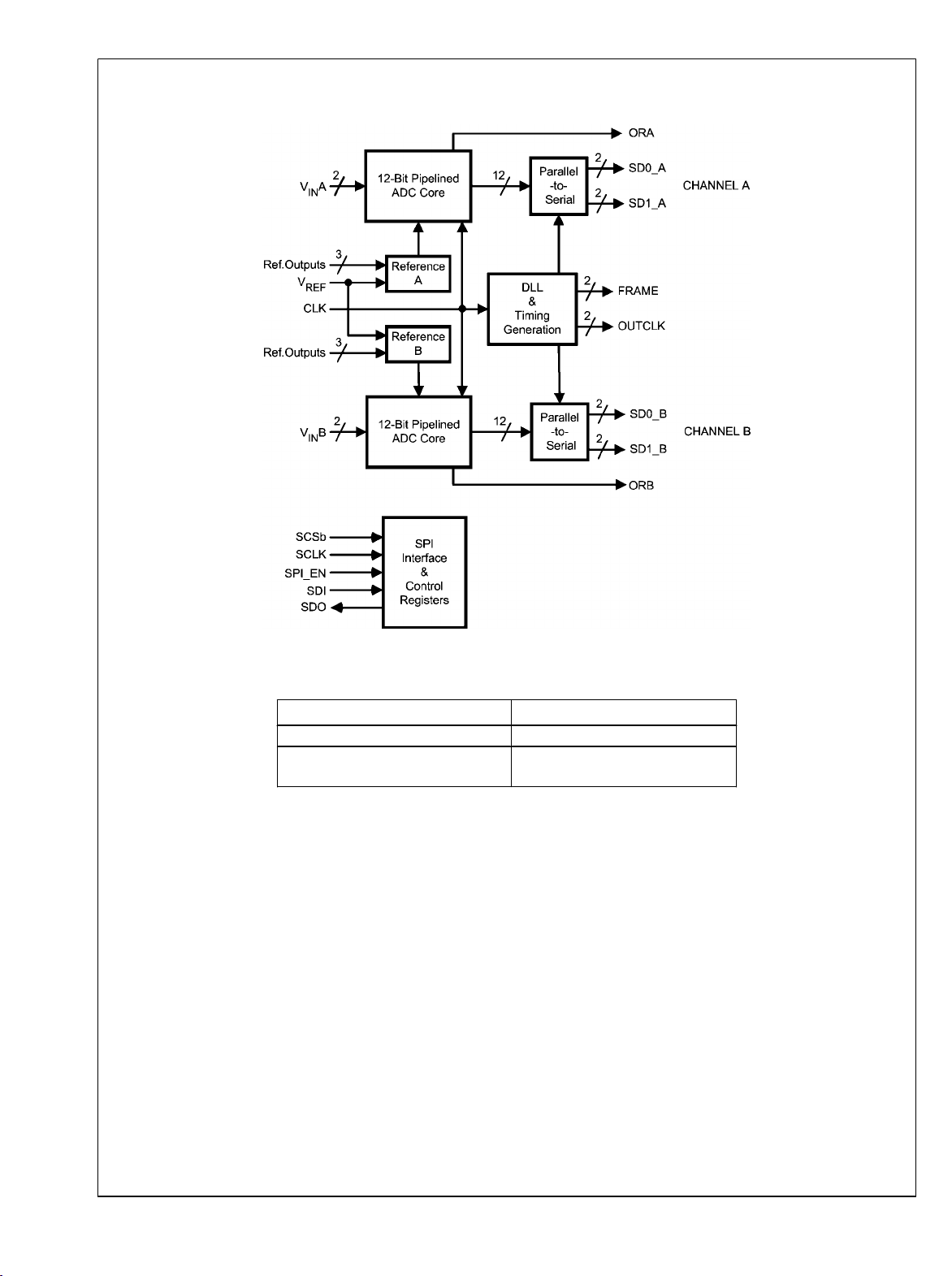
Block Diagram
ADC12DS080
Ordering Information
Industrial (−40°C ≤ TA ≤ +85°C)
30049702
Package
ADC12DS080CISQ 60 Pin LLP
ADC12DS080LFEB Evaluation Board for
Input Frequency < 70 MHz
www.national.com 2
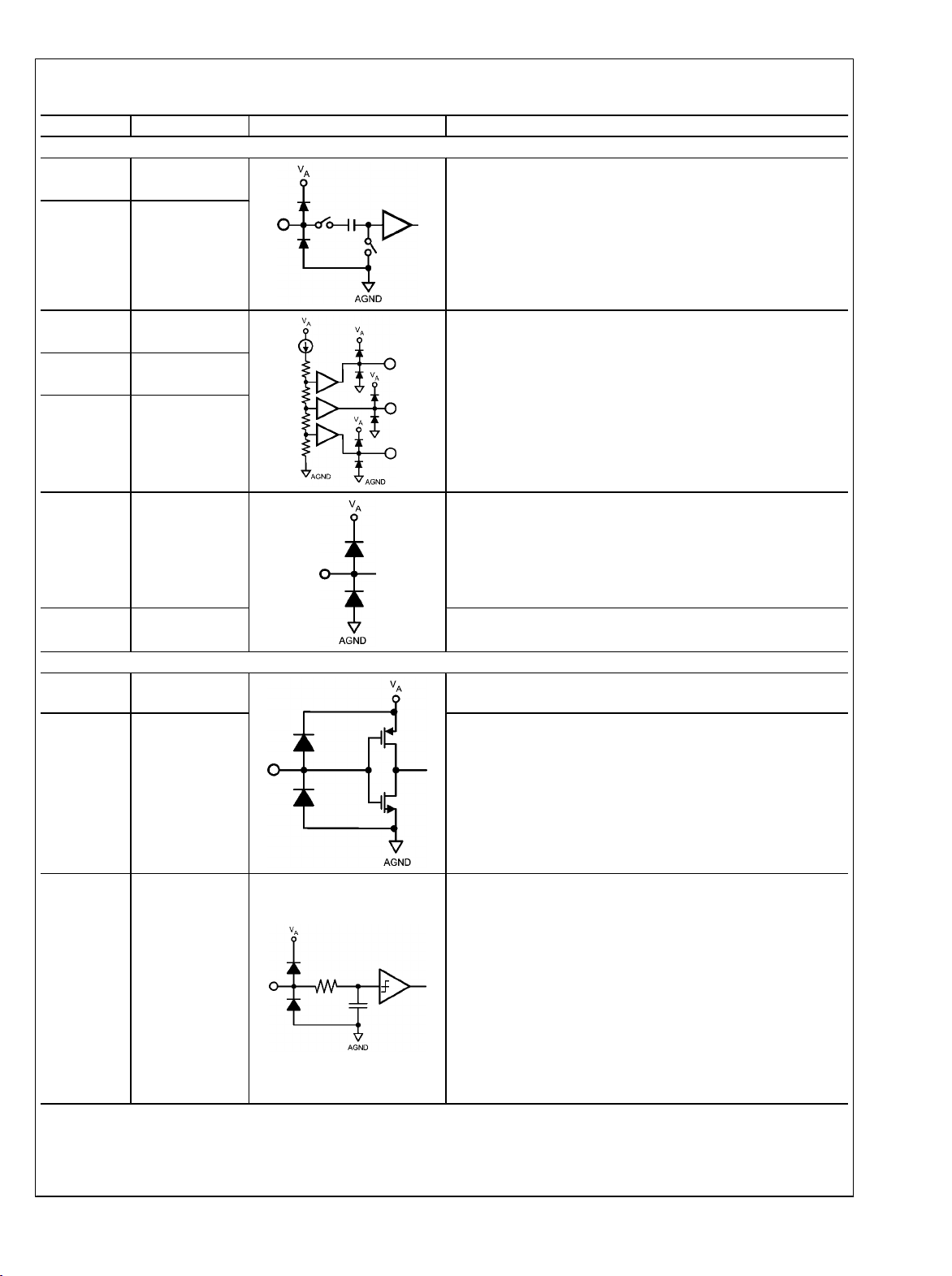
Pin Descriptions and Equivalent Circuits
Pin No. Symbol Equivalent Circuit Description
ANALOG I/O
3
13
2
14
VINA+
VINB+
VINAVINB-
Differential analog input pins. The differential full-scale input signal
level is 2V
with each input pin signal centered on a common
P-P
mode voltage, VCM.
ADC12DS080
5
11
7
9
6
10
59
29 LVDS_Bias
DIGITAL I/O
18 CLK
28 Reset_DLL
VRPA
VRPB
V
CMO
V
CMO
VRNA
VRNB
V
REF
These pins should each be bypassed to AGND with a low ESL
(equivalent series inductance) 0.1 µF capacitor placed very close
A
B
to the pin to minimize stray inductance. An 0201 size 0.1 µF
capacitor should be placed between VRP and VRN as close to the
pins as possible, and a 1 µF capacitor should be placed in parallel.
VRP and VRN should not be loaded. V
may be loaded to 1mA
CMO
for use as a temperature stable 1.5V reference.
It is recommended to use V
to provide the common mode
CMO
voltage, VCM, for the differential analog inputs.
Reference Voltage. This device provides an internally developed
1.2V reference. When using the internal reference, V
should be
REF
decoupled to AGND with a 0.1 µF and a 1µF, low equivalent series
inductance (ESL) capacitor.
This pin may be driven with an external 1.2V reference voltage.
This pin should not be used to source or sink current.
LVDS Driver Bias Resistor is applied from this pin to Analog
Ground. The nominal value is 3.6KΩ
The clock input pin.
The analog inputs are sampled on the rising edge of the clock input.
Reset_DLL input. This pin is normally low. If the input clock
frequency is changed abruptly, the internal timing circuits may
become unlocked. Cycle this pin high for 1 microsecond to re-lock
the DLL. The DLL will lock in several microseconds after
Reset_DLL is asserted.
19 OF/DCS
This is a four-state pin controlling the input clock mode and output
data format.
OF/DCS = VA, output data format is 2's complement without duty
cycle stabilization applied to the input clock
OF/DCS = AGND, output data format is offset binary, without duty
cycle stabilization applied to the input clock.
OF/DCS = (2/3)*VA, output data is 2's complement with duty cycle
stabilization applied to the input clock
OF/DCS = (1/3)*VA, output data is offset binary with duty cycle
stabilization applied to the input clock.
Note: This signal has no effect when SPI_EN is high and the SPI
interface is enabled.
3 www.national.com
Pin No. Symbol Equivalent Circuit Description
This is a two-state input controlling Power Down.
57
ADC12DS080
20
27 TEST
47 WAM
48 DLC
45
44
43
42
PD_A
PD_B
OUTCLK+
OUTCLK-
FRAME+
FRAME-
PD = VA, Power Down is enabled and power dissipation is reduced.
PD = AGND, Normal operation.
Note: This signal has no effect when SPI_EN is high and the SPI
interface is enabled.
Test Mode. When this signal is asserted high, a fixed test pattern
(101001100011 msb->lsb) is sourced at the data outputs.
With this signal deasserted low, the device is in normal operation
mode.
Note: This signal has no effect when SPI_EN is high and the SPI
interface is enabled.
Word Alignment Mode.
In single-lane mode this pin must be set to logic-0.
In dual-lane mode only, when this signal is at logic-0 the serial data
words are offset by half-word. With this signal at logic-1 the serial
data words are aligned with each other.
Note: This signal has no effect when SPI_EN is high and the SPI
interface is enabled.
Dual-Lane Configuration. The dual-lane mode is selected when
this signal is at logic-0. With this signal at logic-1, all data is sourced
on a single lane (SD1_x) for each channel.
Note: This signal has no effect when SPI_EN is high and the SPI
interface is enabled.
Serial Clock. This pair of differential LVDS signals provides the
serial clock that is synchronous with the Serial Data outputs. A bit
of serial data is provided on each of the active serial data outputs
with each falling and rising edge of this clock. This differential
output is always enabled while the device is powered up. In powerdown mode this output is held in logic-low state. A 100-ohm
termination resistor must always be used between this pair of
signals at the far end of the transmission line.
Serial Data Frame. This pair of differential LVDS signals transitions
at the serial data word boundaries. The SD1_A+/- and SD1_B+/output words always begin with the rising edge of the Frame signal.
The falling edge of the Frame signal defines the start of the serial
data word presented on the SD0_A+/- and SD0_B+/- signal pairs
in the Dual-Lane mode. This differential output is always enabled
while the device is powered up. In power-down mode this output is
held in logic-low state. A 100-ohm termination resistor must always
be used between this pair of signals at the far end of the
transmission line.
www.national.com 4

Pin No. Symbol Equivalent Circuit Description
Serial Data Output 1 for Channel A. This is a differential LVDS pair
of signals that carries channel A ADC’s output in serialized form.
The serial data is provided synchronous with the OUTCLK output.
In Single-Lane mode each sample’s output is provided in
38
37
34
33
36
35
32
31
56 SPI_EN
55 SCSb
52 SCLK
54 SDI
SD1_A+
SD1_A-
SD1_B+
SD1_B-
SD0_A+
SD0_A-
SD0_B+
SD0_B-
succession. In Dual-Lane mode every other sample output is
provided on this output. This differential output is always enabled
while the device is powered up. In power-down mode this output
holds the last logic state. A 100-ohm termination resistor must
always be used between this pair of signals at the far end of the
transmission line.
Serial Data Output 1 for Channel B. This is a differential LVDS pair
of signals that carries channel B ADC’s output in serialized form.
The serial data is provided synchronous with the OUTCLK output.
In Single-Lane mode each sample’s output is provided in
succession. In Dual-Lane mode every other sample output is
provided on this output. This differential output is always enabled
while the device is powered up. In power-down mode this output
holds the last logic state. A 100-ohm termination resistor must
always be used between this pair of signals at the far end of the
transmission line.
Serial Data Output 0 for Channel A. This is a differential LVDS pair
of signals that carries channel A ADC’s alternating samples’ output
in serialized form in Dual-Lane mode. The serial data is provided
synchronous with the OUTCLK output. In Single-Lane mode this
differential output is held in high impedance state. This differential
output is always enabled while the device is powered up. In power-
down mode this output holds the last logic state. A 100-ohm
termination resistor must always be used between this pair of
signals at the far end of the transmission line.
Serial Data Output 0 for Channel B. This is a differential LVDS pair
of signals that carries channel B ADC’s alternating samples’ output
in serialized form in Dual-Lane mode. The serial data is provided
synchronous with the OUTCLK output. In Single-Lane mode this
differential output is held in high impedance state. This differential
output is always enabled while the device is powered up. In power-
down mode this output holds the last logic state. A 100-ohm
termination resistor must always be used between this pair of
signals at the far end of the transmission line.
SPI Enable: The SPI interface is enabled when this signal is
asserted high. In this case the direct control pins have no effect.
When this signal is deasserted, the SPI interface is disabled and
the direct control pins are enabled.
Serial Chip Select: While this signal is asserted SCLK is used to
accept serial data present on the SDI input and to source serial
data on the SDO output. When this signal is deasserted, the SDI
input is ignored and the SDO output is in tri-state mode.
Serial Clock: Serial data are shifted into and out of the device
synchronous with this clock signal.
Serial Data-In: Serial data are shifted into the device on this pin
while SCSb signal is asserted.
ADC12DS080
5 www.national.com

Pin No. Symbol Equivalent Circuit Description
Serial Data-Out: Serial data are shifted out of the device on this pin
53 SDO
while SCSb signal is asserted. This output is in tri-state mode when
SCSb is deasserted.
ADC12DS080
46
30
ORA
ORB
Overrange. These CMOS outputs are asserted logic-high when
their respective channel’s data output is out-of-range in either high
or low direction.
DLL_Lock Output. When the internal DLL is locked to the input
CLK, this pin outputs a logic high. If the input CLK is changed
24 DLL_Lock
abruptly, the internal DLL may become unlocked and this pin will
output a logic low. Cycle Reset_DLL (pin 28) to re-lock the DLL to
the input CLK.
ANALOG POWER
8, 16, 17, 58,
60
1, 4, 12, 15,
Exposed Pad
V
A
AGND The ground return for the analog supply.
Positive analog supply pins. These pins should be connected to a
quiet source and be bypassed to AGND with 0.1 µF capacitors
located close to the power pins.
DIGITAL POWER
Positive driver supply pin for the output drivers. This pin should be
26, 40, 50
V
DR
connected to a quiet voltage source and be bypassed to DRGND
with a 0.1 µF capacitor located close to the power pin.
The ground return for the digital output driver supply. This pins
25, 39, 51 DRGND
should be connected to the system digital ground, but not be
connected in close proximity to the ADC's AGND pins.
www.national.com 6

ADC12DS080
Absolute Maximum Ratings (Notes 1, 3)
If Military/Aerospace specified devices are required,
please contact the National Semiconductor Sales Office/
Distributors for availability and specifications.
Supply Voltage (VA, VDR) −0.3V to 4.2V
Voltage on Any Pin
(Not to exceed 4.2V)
Input Current at Any Pin other
than Supply Pins (Note 4)
−0.3V to (VA +0.3V)
±5 mA
Operating Ratings (Notes 1, 3)
Operating Temperature
Supply Voltage (VA=VDR) +2.7V to +3.6V
Clock Duty Cycle
(DCS Enabled) 30/70 %
(DCS disabled) 45/55 %
V
CM
|AGND-DRGND|
−40°C ≤ TA ≤ +85°C
1.4V to 1.6V
≤100mV
Package Input Current (Note 4) ±50 mA
Max Junction Temp (TJ) +150°C
Thermal Resistance (θJA)
30°C/W
ESD Rating
Human Body Model (Note 6) 2500V
Machine Model (Note 6) 250V
Storage Temperature −65°C to +150°C
Soldering process must comply with National
Semiconductor's Reflow Temperature Profile
specifications. Refer to www.national.com/packaging.
(Note 7)
Converter Electrical Characteristics
Unless otherwise specified, the following specifications apply: AGND = DRGND = 0V, VA = VDR = +3.0V, Internal V
f
= 80 MHz, VCM = V
CLK
, CL = 5 pF/pin. Typical values are for TA = 25°C. Boldface limits apply for T
CMO
≤ TA ≤ T
MIN
limits apply for TA = 25°C (Notes 8, 9)
Symbol Parameter Conditions
Typical
(Note 10)
Limits
STATIC CONVERTER CHARACTERISTICS
Resolution with No Missing Codes 12 Bits (min)
INL Integral Non Linearity
DNL Differential Non Linearity
±0.5
±0.25
1.5 LSB (max)
-1.5 LSB (min)
0.5 LSB (max)
-0.5 LSB (min)
PGE Positive Gain Error 0.1 ±1 %FS (max)
NGE Negative Gain Error 0.1 ±1 %FS (max)
V
OFF
Offset Error
0.2 ±0.65 %FS (max)
Under Range Output Code 0 0
Over Range Output Code 4095 4095
REFERENCE AND ANALOG INPUT CHARACTERISTICS
V
CMO
V
CM
C
IN
V
REF
TC V
V
RP
V
RN
Common Mode Output Voltage 1.5
Analog Input Common Mode Voltage 1.5
VIN Input Capacitance (each pin to GND)
(Note 11)
Internal Reference Voltage 1.18
Internal Reference Voltage Tempco
REF
Internal Reference Top 2.0 V
Internal Reference Bottom 1.0 V
Internal Reference Accuracy
EXT
V
REF
External Reference Voltage 1.2
VIN = 1.5 Vdc
± 0.5 V
−40°C ≤ TA ≤ +85°C
(VRP-VRN)
(CLK LOW) 8.5 pF
(CLK HIGH) 3.5 pF
18 ppm/°C
0.97
1.4
1.6
1.4
1.6
1.15
1.21
0.89
1.06
1.176
1.224
= +1.2V,
REF
MAX
(Limits)
V (min)
V (max)
V (min)
V (max)
V (min)
V (max)
V (min)
V (max)
V (min)
V (max)
. All other
Units
7 www.national.com
Dynamic Converter Electrical Characteristics
Unless otherwise specified, the following specifications apply: AGND = DRGND = 0V, VA = VDR = +3.0V, Internal V
f
= 80 MHz, VCM = V
CLK
other limits apply for TA = 25°C (Notes 8, 9)
ADC12DS080
Symbol Parameter Conditions
DYNAMIC CONVERTER CHARACTERISTICS, AIN = -1dBFS
FPBW Full Power Bandwidth -1 dBFS Input, −3 dB Corner 1.0 GHz
SNR Signal-to-Noise Ratio
SFDR Spurious Free Dynamic Range
ENOB Effective Number of Bits
THD Total Harmonic Disortion
H2 Second Harmonic Distortion
H3 Third Harmonic Distortion
SINAD Signal-to-Noise and Distortion Ratio
IMD Intermodulation Distortion
, CL = 5 pF/pin, . Typical values are for TA = 25°C. Boldface limits apply for T
CMO
Typical
(Note 10)
fIN = 10 MHz
fIN = 70 MHz
fIN = 170 MHz
fIN = 10 MHz
fIN = 70 MHz
fIN = 170 MHz
fIN = 10 MHz
fIN = 70 MHz
fIN = 170 MHz
fIN = 10 MHz
fIN = 70 MHz
fIN = 170 MHz
fIN = 10 MHz
fIN = 70 MHz
fIN = 170 MHz
fIN = 10 MHz
fIN = 70 MHz
fIN = 170 MHz
fIN = 10 MHz
fIN = 70 MHz
fIN = 170 MHz
fIN=19.5 and 20.5MHz,
each -7dBFS
71 dBFS
70.5 dBFS
70 68.5 dBFS
88 dBFS
85 dBFS
81 76.5 dBFS
11.5 Bits
11.4 Bits
11.3 10.9 Bits
−86 dBFS
−85 dBFS
−80 -75 dBFS
−90 dBFS
−88 dBFS
−83 -76.5 dBFS
−88 dBFS
−85 dBFS
−81 -76.5 dBFS
70.8 dBFS
70.3 dBFS
69.6 67.6 dBFS
-84 dBFS
MIN
Limits
≤ TA ≤ T
= +1.2V,
REF
(Limits)
(Note 2)
MAX
Units
. All
Logic and Power Supply Electrical Characteristics
Unless otherwise specified, the following specifications apply: AGND = DRGND = 0V, VA = VDR = +3.0V, Internal V
f
= 80 MHz, VCM = V
CLK
limits apply for TA = 25°C (Notes 8, 9)
Symbol Parameter Conditions
DIGITAL INPUT CHARACTERISTICS (CLK, PD_A,PD_B,SCSb,SPI_EN,SCLK,SDI,TEST,WAM,DLC)
V
V
I
IN(1)
I
IN(0)
C
IN(1)
IN(0)
IN
Logical “1” Input Voltage
Logical “0” Input Voltage
Logical “1” Input Current
Logical “0” Input Current VIN = 0V
Digital Input Capacitance 5 pF
DIGITAL OUTPUT CHARACTERISTICS (ORA,ORB,SDO,DLL_Lock)
V
OUT(1)
V
OUT(0)
+I
SC
−I
SC
www.national.com 8
Logical “1” Output Voltage
Logical “0” Output Voltage
Output Short Circuit Source Current V
Output Short Circuit Sink Current
, CL = 5 pF/pin. Typical values are for TA = 25°C. Boldface limits apply for T
CMO
VD = 3.6V
VD = 3.0V
VIN = 3.3V
I
= −0.5 mA
OUT
I
= 1.6 mA
OUT
= 0V
OUT
V
= V
OUT
DR
MIN
Typical
(Note 10)
2.0 V (min)
0.8 V (max)
10
−10 µA
1.2 V (min)
0.4 V (max)
−10
10 mA
≤ TA ≤ T
REF
MAX
Limits
µA
= +1.2V,
. All other
Units
(Limits)
mA

ADC12DS080
Symbol Parameter Conditions
C
OUT
Digital Output Capacitance 5 pF
Typical
(Note 10)
Limits
POWER SUPPLY CHARACTERISTICS
I
A
I
DR
Analog Supply Current
Digital Output Supply Current
Full Operation 204 230 mA (max)
Full Operation 62 70 mA
Power Consumption 800 900 mW (max)
Power Down Power Consumption Clock disabled 30 mW
Timing and AC Characteristics
Unless otherwise specified, the following specifications apply: AGND = DRGND = 0V, VA = VDR = +3.0V, Internal V
f
= 80 MHz, VCM = V
CLK
amplitude. Boldface limits apply for T
Symb Parameter Conditions
Maximum Clock Frequency
Minimum Clock Frequency
, CL = 5 pF/pin. Typical values are for TA = 25°C. Timing measurements are taken at 50% of the signal
CMO
≤ TA ≤ T
MIN
. All other limits apply for TA = 25°C (Notes 8, 9)
MAX
In Single-Lane Mode
In Dual-Lane Mode
In Single-Lane Mode
In Dual-Lane Mode
Typical
(Note 10)
Limits
Single-Lane Mode
t
CONV
Conversion Latency
Dual-Lane, Offset Mode
Dual-Lane, Word Aligned Mode
t
AD
t
AJ
Aperture Delay 0.6 ns
Aperture Jitter 0.1
65
80
25
52.5
7.5
8
9
REF
MHz (max)
Clock Cycles
Units
(Limits)
= +1.2V,
Units
(Limits)
MHz (min)
ps rms
Serial Control Interface Timing and AC Characteristics
Unless otherwise specified, the following specifications apply: AGND = DRGND = 0V, VA = VDR = +3.0V, Internal V
f
= 80 MHz, VCM = V
CLK
amplitude. Boldface limits apply for T
Symb Parameter Conditions
f
SCLK
t
PH
t
PL
t
SU
t
H
t
ODZ
t
OZD
t
OD
t
CSS
t
CSH
t
IAG
Serial Clock Frequency
SCLK Pulse Width - High % of SCLK Period
SCLK Pulse Width - Low % of SCLK Period
SDI Setup Time 5 ns (min)
SDI Hold Time 5 ns (min)
SDO Driven-to-Tri-State Time 40 50 ns (max)
SDO Tri-State-to-Driven Time 15 20 ns (max)
SDO Output Delay Time 15 20 ns (max)
SCSb Setup Time 5 10 ns (min)
SCSb Hold Time 5 10 ns (min)
Inter-Access Gap
, CL = 5 pF/pin. Typical values are for TA = 25°C. Timing measurements are taken at 50% of the signal
CMO
≤ TA ≤ T
MIN
. All other limits apply for TA = 25°C (Notes 8, 9)
MAX
f
= f
CLK
/10
SCLK
Minimum time SCSb must be deasserted
between accesses
Typical
(Note 10)
Limits
8 MHz (max)
3
40
60
40
60
= +1.2V,
REF
Units
(Limits)
% (min)
% (max)
% (min)
% (max)
Cycles of
SCLK
9 www.national.com

LVDS Electrical Characteristics
Unless otherwise specified, the following specifications apply: AGND = DRGND = 0V, VA = VDR = +3.0V, Internal V
f
= 80 MHz, VCM = V
CLK
amplitude. Boldface limits apply for T
ADC12DS080
Symbol Parameter Conditions
LVDS DC CHARACTERISTICS
V
OD
delta
V
OD
V
OS
delta V
Output Differential Voltage
(SDO+) - (SDO-)
Output Differential Voltage Unbalance
Offset Voltage
Offset Voltage Unbalance
OS
IOS Output Short Circuit Current
LVDS OUTPUT TIMING AND SWITCHING CHARACTERISTICS
t
DP
t
HO
t
SUO
t
FP
t
FDC
t
DFS
t
ODOR
Output Data Bit Period Dual-Lane Mode 2.08 ns
Output Data Edge to Output Clock Edge
Hold Time(Note 12)
Output Data Edge to Output Clock Edge
Set-Up Time(Note 12)
Frame Period Dual-Lane Mode 25 ns
Frame Clock Duty Cycle(Note 12) 50
Data Edge to Frame Edge Skew 50% to 50% 15 ps
Output Delay of OR output
, CL = 5 pF/pin. Typical values are for TA = 25°C. Timing measurements are taken at 50% of the signal
CMO
≤ TA ≤ T
MIN
. All other limits apply for TA = 25°C (Notes 8, 9)
MAX
Typical
(Note 10)
RL = 100Ω
RL = 100Ω
RL = 100Ω
RL = 100Ω
DO = 0V, VIN = 1.1V,
350
±25 mV (max)
1.25
±25 mV (max)
-10 mA (max)
Dual-Lane Mode 990 550 ps (min)
Dual-Lane Mode 1100 600 ps (min)
From rising edge of CLK to ORA/ORB
valid
4 ns
Limits
250
450
1.125
1.375
45
55
= +1.2V,
REF
mV (max)
Units
(Limits)
mV (min)
V (min)
V (max)
% (min)
% (max)
Note 1: Absolute Maximum Ratings indicate limits beyond which damage to the device may occur. Operating Ratings indicate conditions for which the device is
guaranteed to be functional, but do not guarantee specific performance limits. For guaranteed specifications and test conditions, see the Electrical Characteristics.
The guaranteed specifications apply only for the test conditions listed. Some performance characteristics may degrade when the device is not operated under
the listed test conditions. Operation of the device beyond the maximum Operating Ratings is not recommended.
Note 2: This parameter is specified in units of dBFS - indicating the value that would be attained with a full-scale input signal.
Note 3: All voltages are measured with respect to GND = AGND = DRGND = 0V, unless otherwise specified.
Note 4: When the input voltage at any pin exceeds the power supplies (that is, VIN < AGND, or VIN > VA), the current at that pin should be limited to ±5 mA. The
±50 mA maximum package input current rating limits the number of pins that can safely exceed the power supplies with an input current of ±5 mA to 10.
Note 5: The maximum allowable power dissipation is dictated by T
can be calculated using the formula P
operated in a severe fault condition (e.g. when input or output pins are driven beyond the power supply voltages, or the power supply polarity is reversed). Such
conditions should always be avoided.
Note 6: Human Body Model is 100 pF discharged through a 1.5 kΩ resistor. Machine Model is 220 pF discharged through 0 Ω
Note 7: Reflow temperature profiles are different for lead-free and non-lead-free packages.
Note 8: The inputs are protected as shown below. Input voltage magnitudes above VA or below GND will not damage this device, provided current is limited per
D,max
= (T
- TA )/θJA. The values for maximum power dissipation listed above will be reached only when the device is
J,max
, the junction-to-ambient thermal resistance, (θJA), and the ambient temperature, (TA), and
J,max
(Note 4). However, errors in the A/D conversion can occur if the input goes above 2.6V or below GND as described in the Operating Ratings section.
30049711
Note 9: With a full scale differential input of 2V
Note 10: Typical figures are at TA = 25°C and represent most likely parametric norms at the time of product characterization. The typical specifications are not
guaranteed.
Note 11: The input capacitance is the sum of the package/pin capacitance and the sample and hold circuit capacitance.
Note 12: This parameter is guaranteed by design and/or characterization and is not tested in production.
, the 12-bit LSB is 488 µV.
P-P
www.national.com 10

ADC12DS080
Specification Definitions
APERTURE DELAY is the time after the falling edge of the
clock to when the input signal is acquired or held for conversion.
APERTURE JITTER (APERTURE UNCERTAINTY) is the
variation in aperture delay from sample to sample. Aperture
jitter manifests itself as noise in the output.
CLOCK DUTY CYCLE is the ratio of the time during one cycle
that a repetitive digital waveform is high to the total time of
one period. The specification here refers to the ADC clock
input signal.
COMMON MODE VOLTAGE (VCM) is the common DC voltage applied to both input terminals of the ADC.
CONVERSION LATENCY is the number of clock cycles between initiation of conversion and when that data is presented
to the output driver stage. Data for any given sample is available at the output pins the Pipeline Delay plus the Output
Delay after the sample is taken. New data is available at every
clock cycle, but the data lags the conversion by the pipeline
delay.
CROSSTALK is coupling of energy from one channel into the
other channel.
DIFFERENTIAL NON-LINEARITY (DNL) is the measure of
the maximum deviation from the ideal step size of 1 LSB.
EFFECTIVE NUMBER OF BITS (ENOB, or EFFECTIVE
BITS) is another method of specifying Signal-to-Noise and
Distortion Ratio or SINAD. ENOB is defined as (SINAD -
1.76) / 6.02 and says that the converter is equivalent to a
perfect ADC of this (ENOB) number of bits.
FULL POWER BANDWIDTH is a measure of the frequency
at which the reconstructed output fundamental drops 3 dB
below its low frequency value for a full scale input.
GAIN ERROR is the deviation from the ideal slope of the
transfer function. It can be calculated as:
Gain Error = Positive Full Scale Error − Negative Full Scale
Error
It can also be expressed as Positive Gain Error and Negative
Gain Error, which are calculated as:
PGE = Positive Full Scale Error - Offset Error
NGE = Offset Error - Negative Full Scale Error
INTEGRAL NON LINEARITY (INL) is a measure of the deviation of each individual code from a best fit straight line. The
deviation of any given code from this straight line is measured
from the center of that code value.
INTERMODULATION DISTORTION (IMD) is the creation of
additional spectral components as a result of two sinusoidal
frequencies being applied to the ADC input at the same time.
It is defined as the ratio of the power in the intermodulation
products to the total power in the original frequencies. IMD is
usually expressed in dBFS.
LSB (LEAST SIGNIFICANT BIT) is the bit that has the smallest value or weight of all bits. This value is VFS/2n, where
“VFS” is the full scale input voltage and “n” is the ADC resolution in bits.
LVDS Differential Output Voltage (VOD) is the absolute value of the difference between the differential output pair voltages (VD+ and VD-), each measured with respect to ground.
MISSING CODES are those output codes that will never appear at the ADC outputs. The ADC is guaranteed not to have
any missing codes.
MSB (MOST SIGNIFICANT BIT) is the bit that has the largest
value or weight. Its value is one half of full scale.
NEGATIVE FULL SCALE ERROR is the difference between
the actual first code transition and its ideal value of ½ LSB
above negative full scale.
OFFSET ERROR is the difference between the two input
voltages [(VIN+) – (VIN-)] required to cause a transition from
code 2047 to 2048.
OUTPUT DELAY is the time delay after the falling edge of the
clock before the data update is presented at the output pins.
PIPELINE DELAY (LATENCY) See CONVERSION LATENCY.
POSITIVE FULL SCALE ERROR is the difference between
the actual last code transition and its ideal value of 1½ LSB
below positive full scale.
POWER SUPPLY REJECTION RATIO (PSRR) is a measure
of how well the ADC rejects a change in the power supply
voltage. PSRR is the ratio of the Full-Scale output of the ADC
with the supply at the minimum DC supply limit to the FullScale output of the ADC with the supply at the maximum DC
supply limit, expressed in dB.
SIGNAL TO NOISE RATIO (SNR) is the ratio, expressed in
dB, of the rms value of the input signal to the rms value of the
sum of all other spectral components below one-half the sampling frequency, not including harmonics or DC.
SIGNAL TO NOISE PLUS DISTORTION (S/N+D or
SINAD) Is the ratio, expressed in dB, of the rms value of the
input signal to the rms value of all of the other spectral components below half the clock frequency, including harmonics
but excluding d.c.
SPURIOUS FREE DYNAMIC RANGE (SFDR) is the difference, expressed in dB, between the rms values of the input
signal and the peak spurious signal, where a spurious signal
is any signal present in the output spectrum that is not present
at the input.
TOTAL HARMONIC DISTORTION (THD) is the ratio, expressed in dB, of the rms total of the first six harmonic levels
at the output to the level of the fundamental at the output. THD
is calculated as
where f1 is the RMS power of the fundamental (output) frequency and f2 through f7 are the RMS power of the first six
harmonic frequencies in the output spectrum.
SECOND HARMONIC DISTORTION (2ND HARM) is the difference expressed in dB, between the RMS power in the input
frequency at the output and the power in its 2nd harmonic
level at the output.
THIRD HARMONIC DISTORTION (3RD HARM) is the difference, expressed in dB, between the RMS power in the
input frequency at the output and the power in its 3rd harmonic
level at the output.
11 www.national.com

Timing Diagrams
ADC12DS080
Serial Output Data Timing
FIGURE 1.
30049714
FIGURE 2. Serial Output Data Format in Single-Lane Mode
www.national.com 12
30049717

ADC12DS080
FIGURE 3. Serial Output Data Format in Dual-Lane Mode
13 www.national.com
30049718

Transfer Characteristic
ADC12DS080
FIGURE 4. Transfer Characteristic
30049710
www.national.com 14
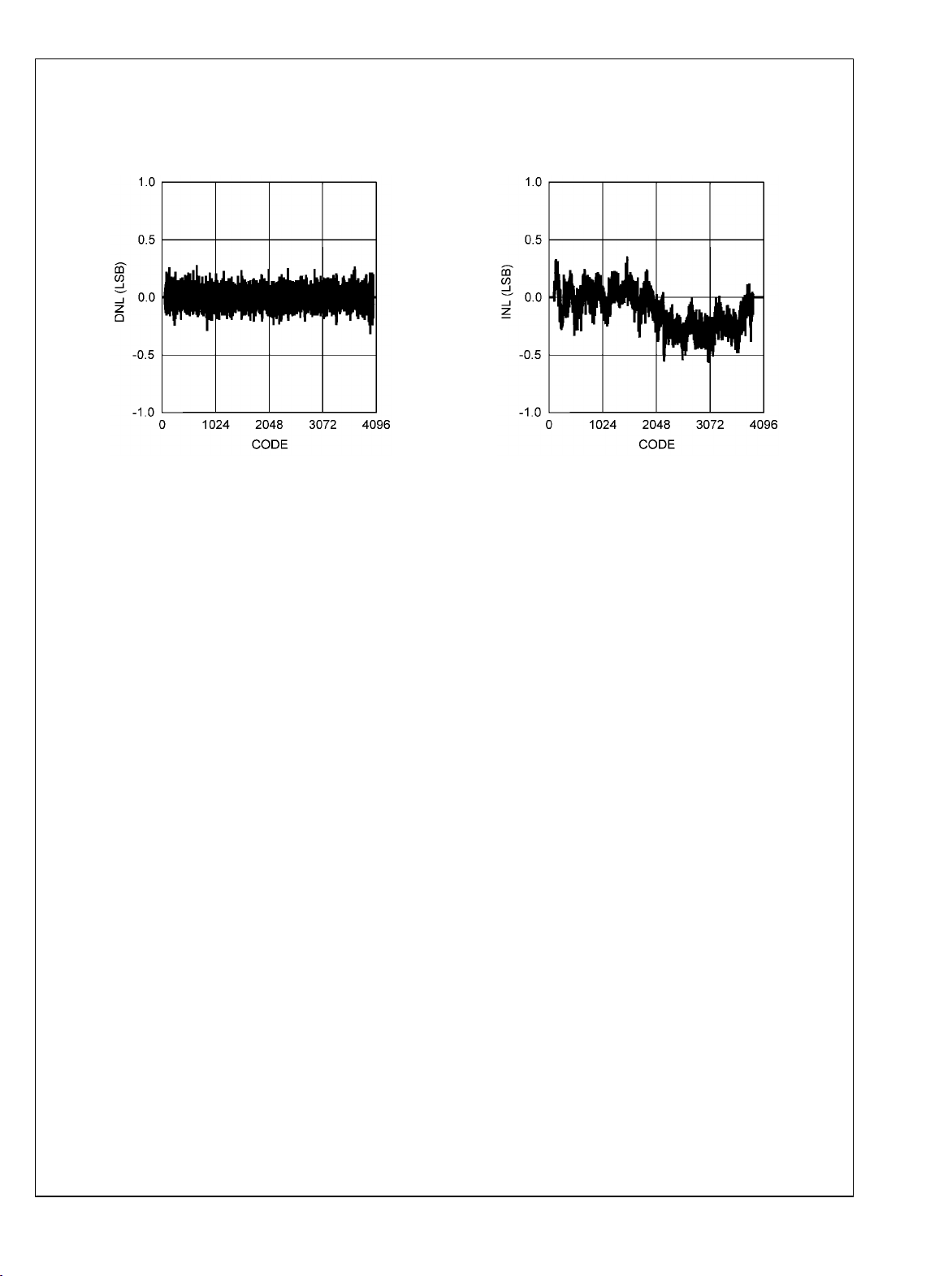
Typical Performance Characteristics DNL, INL Unless otherwise specified, the following
specifications apply: AGND = DRGND = 0V, VA = VDR = +3.0V, Internal V
disabled, VCM = V
, TA = 25°C.
CMO
= +1.2V, f
REF
= 80 MHz, 50% Duty Cycle, DCS
CLK
ADC12DS080
DNL
30049741
INL
30049742
15 www.national.com

Typical Performance Characteristics Unless otherwise specified, the following specifications apply:
AGND = DRGND = 0V, VA = VDR = +3.0V, Internal V
fIN = 10 MHz, TA = 25°C.
= +1.2V, f
REF
= 80 MHz, 50% Duty Cycle, DCS disabled, VCM = V
CLK
CMO
,
ADC12DS080
SNR, SINAD, SFDR vs. Clock Duty Cycle
SNR, SINAD, SFDR vs. V
A
30049751
Distortion vs. V
A
30049752
Distortion vs. Clock Duty Cycle
30049757
SNR, SINAD, SFDR vs. Clock Duty Cycle, DCS Enabled
30049759
www.national.com 16
30049758
Distortion vs. Clock Duty Cycle, DCS Enabled
30049760

ADC12DS080
Spectral Response @ 10 MHz Input
Spectral Response @ 170 MHz Input
30049768
Spectral Response @ 70 MHz Input
30049769
IMD, fIN1 = 20 MHz, fIN2 = 21 MHz
30049770
30049771
17 www.national.com

Functional Description
Operating on a single +3.3V supply, the ADC12DS080 digitizes two differential analog input signals to 12 bits, using a
differential pipelined architecture with error correction circuitry
and an on-chip sample-and-hold circuit to ensure maximum
ADC12DS080
performance. The user has the choice of using an internal
1.2V stable reference, or using an external 1.2V reference.
Any external reference is buffered on-chip to ease the task of
driving that pin. Duty cycle stabilization and output data format
are selectable using the quad state function OF/DCS pin (pin
19). The output data can be set for offset binary or two's complement.
Applications Information
1.0 OPERATING CONDITIONS
We recommend that the following conditions be observed for
operation of the ADC12DS080:
2.7V ≤ VA ≤ 3.6V
2.7V ≤ VDR ≤ V
25 MHz ≤ f
CLK
1.2V internal reference
V
= 1.2V (for an external reference)
REF
VCM = 1.5V (from V
2.0 ANALOG INPUTS
2.1 Signal Inputs
A
≤ 105 MHz
CMO
)
For single frequency sine waves the full scale error in LSB
can be described as approximately
EFS = 4096 ( 1 - sin (90° + dev))
Where dev is the angular difference in degrees between the
two signals having a 180° relative phase relationship to each
other (see Figure 6). For single frequency inputs, angular errors result in a reduction of the effective full scale input. For
complex waveforms, however, angular errors will result in
distortion.
30049781
FIGURE 6. Angular Errors Between the Two Input Signals
Will Reduce the Output Level or Cause Distortion
It is recommended to drive the analog inputs with a source
impedance less than 100Ω. Matching the source impedance
for the differential inputs will improve even ordered harmonic
performance (particularly second harmonic).
Table 1 indicates the input to output relationship of the ADC12DS080.
2.1.1 Differential Analog Input Pins
The ADC12DS080 has a pair of analog signal input pins for
each of two channels. VIN+ and VIN− form a differential input
pair. The input signal, VIN, is defined as
VIN = (VIN+) – (VIN−)
Figure 5 shows the expected input signal range. Note that the
common mode input voltage, VCM, should be 1.5V. Using
V
(pins 7,9) for VCM will ensure the proper input common
CMO
mode level for the analog input signal. The positive peaks of
the individual input signals should each never exceed 2.6V.
Each analog input pin of the differential pair should have a
maximum peak-to-peak voltage of 1V, be 180° out of phase
with each other and be centered around VCM.The peak-topeak voltage swing at each analog input pin should not exceed the 1V or the output data will be clipped.
30049780
FIGURE 5. Expected Input Signal Range
www.national.com 18

TABLE 1. Input to Output Relationship
ADC12DS080
V
VCM − V
VCM − V
V
VCM + V
VCM + V
+
IN
/2 VCM + V
REF
/4 VCM + V
REF
CM
/4 VCM − V
REF
/2 VCM − V
REF
V
−
IN
/2
REF
/4
REF
V
CM
/4
REF
/2
REF
Binary Output 2’s Complement Output
0000 0000 0000 1000 0000 0000 Negative Full-Scale
0100 0000 0000 1100 0000 0000
1000 0000 0000 0000 0000 0000 Mid-Scale
1100 0000 0000 0100 0000 0000
1111 1111 1111 0111 1111 1111 Positive Full-Scale
2.1.2 Driving the Analog Inputs
The VIN+ and the VIN− inputs of the ADC12DS080 have an
internal sample-and-hold circuit which consists of an analog
switch followed by a switched-capacitor amplifier.
FIGURE 7. Low Input Frequency Transformer Drive Circuit
Figure 7 and Figure 8 show examples of single-ended to differential conversion circuits. The circuit in Figure 7 works well
for input frequencies up to approximately 70MHz, while the
circuit in Figure 8 works well above 70MHz.
30049782
FIGURE 8. High Input Frequency Transformer Drive Circuit
One short-coming of using a transformer to achieve the single-ended to differential conversion is that most RF transformers have poor low frequency performance. A differential
amplifier can be used to drive the analog inputs for low frequency applications. The amplifier must be fast enough to
settle from the charging glitches on the analog input resulting
from the sample-and-hold operation before the clock goes
high and the sample is passed to the ADC core.
2.1.3 Input Common Mode Voltage
The input common mode voltage, VCM, should be in the range
of 1.4V to 1.6V and be a value such that the peak excursions
of the analog signal do not go more negative than ground or
more positive than 2.6V. It is recommended to use V
7,9) as the input common mode voltage.
CMO
(pins
2.2 Reference Pins
The ADC12DS080 is designed to operate with an internal or
external 1.2V reference. The internal 1.2 Volt reference is the
default condition when no external reference input is applied
to the V
pin. If a voltage is applied to the V
REF
pin, then
REF
30049783
that voltage is used for the reference. The V
always be bypassed to ground with a 0.1 µF capacitor close
pin should
REF
to the reference input pin.
It is important that all grounds associated with the reference
voltage and the analog input signal make connection to the
ground plane at a single, quiet point to minimize the effects of
noise currents in the ground path.
The Reference Bypass Pins (VRP, V
nels A and B are made available for bypass purposes. These
, and VRN) for chan-
CMO
pins should each be bypassed to AGND with a low ESL
(equivalent series inductance) 1 µF capacitor placed very
close to the pin to minimize stray inductance. A 0.1 µF capacitor should be placed between VRP and VRN as close to
the pins as possible, and a 1 µF capacitor should be placed
in parallel. This configuration is shown in Figure 9. It is necessary to avoid reference oscillation, which could result in
reduced SFDR and/or SNR. V
use as a temperature stable 1.5V reference. The remaining
may be loaded to 1mA for
CMO
pins should not be loaded.
Smaller capacitor values than those specified will allow faster
recovery from the power down mode, but may result in de-
19 www.national.com

graded noise performance. Loading any of these pins, other
than V
may result in performance degradation.
CMO
The nominal voltages for the reference bypass pins are as
follows:
V
= 1.5 V
ADC12DS080
CMO
VRP = 2.0 V
VRN = 1.0 V
2.3 OF/DCS Pin
Duty cycle stabilization and output data format are selectable
using this quad state function pin. When enabled, duty cycle
stabilization can compensate for clock inputs with duty cycles
ranging from 30% to 70% and generate a stable internal clock,
improving the performance of the part. With OF/DCS = VA the
output data format is 2's complement and duty cycle stabilization is not used. With OF/DCS = AGND the output data
format is offset binary and duty cycle stabilization is not used.
With OF/DCS = (2/3)*VA the output data format is 2's complement and duty cycle stabilization is applied to the clock. If
OF/DCS is (1/3)*VA the output data format is offset binary and
duty cycle stabilization is applied to the clock. While the sense
of this pin may be changed "on the fly," doing this is not recommended as the output data could be erroneous for a few
clock cycles after this change is made.
Note: This signal has no effect when SPI_EN is high and the
serial control interface is enabled.
3.0 DIGITAL INPUTS
Digital CMOS compatible inputs consist of CLK, and PD_A,
PD_B, Reset_DLL, DLC, TEST, WAM, SPI_EN, SCSb,
SCLK, and SDI.
3.1 Clock Input
The CLK controls the timing of the sampling process. To
achieve the optimum noise performance, the clock input
should be driven with a stable, low jitter clock signal in the
range indicated in the Electrical Table. The clock input signal
should also have a short transition region. This can be
achieved by passing a low-jitter sinusoidal clock source
through a high speed buffer gate. The trace carrying the clock
signal should be as short as possible and should not cross
any other signal line, analog or digital, not even at 90°.
The clock signal also drives an internal state machine. If the
clock is interrupted, or its frequency is too low, the charge on
the internal capacitors can dissipate to the point where the
accuracy of the output data will degrade. This is what limits
the minimum sample rate.
The clock line should be terminated at its source in the characteristic impedance of that line. Take care to maintain a
constant clock line impedance throughout the length of the
line. Refer to Application Note AN-905 for information on setting characteristic impedance.
It is highly desirable that the the source driving the ADC clock
pins only drive that pin. However, if that source is used to drive
other devices, then each driven pin should be AC terminated
with a series RC to ground, such that the resistor value is
equal to the characteristic impedance of the clock line and the
capacitor value is
where tPD is the signal propagation rate down the clock line,
"L" is the line length and ZO is the characteristic impedance
of the clock line. This termination should be as close as pos-
sible to the ADC clock pin but beyond it as seen from the clock
source. Typical tPD is about 150 ps/inch (60 ps/cm) on FR-4
board material. The units of "L" and tPD should be the same
(inches or centimeters).
The duty cycle of the clock signal can affect the performance
of the A/D Converter. Because achieving a precise duty cycle
is difficult, the ADC12DS080 has a Duty Cycle Stabilizer.
3.2 Power-Down (PD_A and PD_B)
The PD_A and PD_B pins, when high, hold the respective
channel of the ADC12DS080 in a power-down mode to conserve power when that channel is not being used. The channels may be powered down individually or together. The data
in the pipeline is corrupted while in the power down mode.
The Power Down Mode Exit Cycle time is determined by the
value of the components on the reference bypass pins
( VRP, V
the Power Down mode and must be recharged by on-chip
and VRN ). These capacitors lose their charge in
CMO
circuitry before conversions can be accurate. Smaller capacitor values allow slightly faster recovery from the power down
mode, but can result in a reduction in SNR, SINAD and ENOB
performance.
Note: This signal has no effect when SPI_EN is high and the
serial control interface is enabled.
3.3 Reset_DLL
This pin is normally low. If the input clock frequency is
changed abruptly, the internal timing circuits may become
unlocked. Cycle this pin high for 1 microsecond to re-lock the
DLL. The DLL will lock in several microseconds after
Reset_DLL is asserted.
3.4 DLC
This pin sets the output data configuration. With this signal at
logic-1, all data is sourced on a single lane (SD1_x) for each
channel. When this signal is at logic-0, the data is sourced on
dual lanes (SD0_x and SD1_x) for each channel. This simplifies data capture at higher data rates.
Note: This signal has no effect when SPI_EN is high and the
SPI interface is enabled.
3.5 TEST
When this signal is asserted high, a fixed test pattern
(101001100011 msb->lsb) is sourced at the data outputs.
When low, the ADC is in normal operation. The user may
specify a custom test pattern via the serial control interface.
Note: This signal has no effect when SPI_EN is high and the
SPI interface is enabled.
3.6 WAM
In dual-lane mode only, when this signal is at logic-0 the serial
data words are offset by half-word. With this signal at logic-1
the serial data words are aligned with each other. In single
lane mode this pin must be set to logic-0.
Note: This signal has no effect when SPI_EN is high and the
SPI interface is enabled.
3.7 SPI_EN
The SPI interface is enabled when this signal is asserted high.
In this case the direct control pins (OF/DCS, PD_A, PD_B,
DLC, WAM, TEST) have no effect. When this signal is deasserted, the SPI interface is disabled and the direct control
pins are enabled.
www.national.com 20

ADC12DS080
3.8 SCSb, SDI, SCLK
These pins are part of the SPI interface. See Section 5.0 for
more information.
4.0 DIGITAL OUTPUTS
Digital outputs consist of six LVDS signal pairs (SD0_A,
SD1_A, SD0_B, SD1_B, OUTCLK, FRAME) and CMOS logic
outputs ORA, ORB, DLL_Lock, and SDO.
4.1 LVDS Outputs
The digital data for each channel is provided in a serial format.
Two modes of operation are available for the serial data format. Single-lane serial format (shown in Figure 2) uses one
set of differential data signals per channel. Dual-lane serial
format (shown in Figure 3) uses two sets of differential data
signals per channel in order to slow down the data and clock
frequency by a factor of 2. At slower rates of operation (typically below 65 MSPS) the single-lane mode may be the most
efficient to use. At higher rates the user may want to employ
the dual-lane scheme. In either case DDR-type clocking is
used. For each data channel, an overrange indication is also
provided. The OR signal is updated with each frame of data.
4.2 ORA, ORB
These CMOS outputs are asserted logic-high when their respective channel’s data output is out-of-range in either high
or low direction.
4.3 DLL_Lock
When the internal DLL is locked to the input CLK, this pin
outputs a logic high. If the input CLK is changed abruptly, the
internal DLL may become unlocked and this pin will output a
logic low. Cycle Reset_DLL to re-lock the DLL to the input
CLK.
4.4 SDO
This pin is part of the SPI interface. See Section 5.0 for more
information.
FIGURE 9. Application Circuit
5.0 Serial Control Interface
The ADC12DS080 has a serial interface that allows access
to the control registers. The serial interface is a generic 4-wire
synchronous interface that is compatible with SPI type interfaces that are used on many microcontrollers and DSP controllers.
30049785
The ADC's input clock must be running for the Serial Control
Interface to operate. It is enabled when the SPI_EN (pin 56)
signal is asserted high. In this case the direct control pins (OF/
DCS, PD_A, PD_B, DLC, WAM, TEST) have no effect. When
this signal is deasserted, the SPI interface is disabled and the
direct control pins are enabled.
21 www.national.com

Each serial interface access cycle is exactly 16 bits long. Fig-
ure 10 shows the access protocol used by this interface. Each
signal's function is described below. The Read Timing is
ADC12DS080
shown in Figure 11, while the Write Timing is shown in Figure
12
FIGURE 10. Serial Interface Protocol
SCLK: Used to register the input data (SDI) on the rising
edge; and to source the output data (SDO) on the falling edge.
User may disable clock and hold it in the low-state, as long as
clock pulse-width min spec is not violated when clock is enabled or disabled.
SCSb: Serial Interface Chip Select. Each assertion starts a
new register access - i.e., the SDATA field protocol is required. The user is required to deassert this signal after the
16th clock. If the SCSb is deasserted before the 16th clock,
no address or data write will occur. The rising edge captures
the address just shifted-in and, in the case of a write operation, writes the addressed register. There is a minimum pulsewidth requirement for the deasserted pulse - which is
specified in the Electrical Specifications section.
SDI: Serial Data. Must observe setup/hold requirements with
respect to the SCLK. Each cycle is 16-bits long.
30049719
R/Wb: A value of '1' indicates a read operation, while a
value of '0' indicates a write operation.
Reserved: Reserved for future use. Must be set to 0.
ADDR: Up to 3 registers can be addressed.
DATA: In a write operation the value in this field will be
written to the register addressed in this cycle
when SCSb is deasserted. In a read operation
this field is ignored.
SDO: This output is normally at TRI-STATE and is driven only
when SCSb is asserted. Upon SCSb assertion, contents of
the register addressed during the first byte are shifted out with
the second 8 SCLK falling edges. Upon power-up, the default
register address is 00h.
www.national.com 22

FIGURE 11. Read Timing
ADC12DS080
30049716
FIGURE 12. Write Timing
Device Control Register, Address 0h
7 6 5 4 3 2 1 0
OM DLC DCS OF WAM PD_A PD_B
Reset State : 08h
Bits (7:6) Operational Mode
0 0 Normal Operation.
0 1 Test Output mode. A fixed test pattern
(1010011000111msb->lsb) is sourced at the data
outputs.
1 0 Test Output mode. Data pattern defined by
user in registers 01h and 02h is sourced at data
outputs.
1 1 Reserved.
Bit 5 Data Lane Configuration. When this bit is set to '0',
the serial data interface is configured for dual-lane
mode where the data words are output on two data
outputs (SD1 and SD0) at half the rate of the
single-lane interface. When this bit is set to ‘1’,
serial data is output on the SD1 output only and
the SD0 outputs are held in a high-impedance
state
Bit 4 Duty Cycle Stabilizer. When this bit is set to '0' the
DCS is off. When this bit is set to ‘1’, the DCS is
on.
30049715
Bit 3 Output Data Format. When this bit is set to ‘1’ the
data output is in the “twos complement” form.
When this bit is set to ‘0’ the data output is in the
“offset binary” form.
Bit 2 Word Alignment Mode.
This bit must be set to '0' in the single-lane mode
of operation.
In dual-lane mode, when this bit is set to '0' the
serial data words are offset by half-word. This
gives the least latency through the device. When
this bit is set to '1' the serial data words are in
word-aligned mode. In this mode the serial data
on the SD1 lane is additionally delayed by one
CLK cycle. (Refer to Figure 3).
Bit 1 Power-Down Channel A. When this bit is set to '1',
Channel A is in power-down state and Normal
operation is suspended.
Bit 0 Power-Down Channel B. When this bit is set to '1',
Channel B is in power-down state and Normal
operation is suspended.
User Test Pattern Register 0, Address 1h
7 6 5 4 3 2 1 0
Reserved User Test Pattern (13:6)
23 www.national.com

Reset State : 00h
Bits (7:6) Reserved. Must be set to '0'.
Bits (5:0) User Test Pattern. Most-significant 6 bits of the
12-bit pattern that will be sourced out of the data
ADC12DS080
outputs in Test Output Mode.
User Test Pattern Register 1, Address 2h
7 6 5 4 3 2 1 0
User Test Pattern (5:0) Reserved
Reset State : 00h
Bits (7:2) User Test Pattern. Least-significant 6 bits of the
12-bit pattern that will be sourced out of the data
outputs in Test Output Mode.
Bits (1:0) Reserved. Must be set to '0'.
6.0 POWER SUPPLY CONSIDERATIONS
The power supply pins should be bypassed with a 0.1 µF capacitor and with a 100 pF ceramic chip capacitor close to each
power pin. Leadless chip capacitors are preferred because
they have low series inductance.
As is the case with all high-speed converters, the ADC12DS080 is sensitive to power supply noise. Accordingly,
the noise on the analog supply pin should be kept below 100
mV
.
P-P
No pin should ever have a voltage on it that is in excess of the
supply voltages, not even on a transient basis. Be especially
careful of this during power turn on and turn off.
7.0 LAYOUT AND GROUNDING
Proper grounding and proper routing of all signals are essential to ensure accurate conversion. Maintaining separate analog and digital areas of the board, with the ADC12DS080
between these areas, is required to achieve specified performance.
Capacitive coupling between the typically noisy digital circuitry and the sensitive analog circuitry can lead to poor performance. The solution is to keep the analog circuitry separated
from the digital circuitry, and to keep the clock line as short as
possible.
Since digital switching transients are composed largely of
high frequency components, total ground plane copper
weight will have little effect upon the logic-generated noise.
This is because of the skin effect. Total surface area is more
important than is total ground plane area.
Generally, analog and digital lines should cross each other at
90° to avoid crosstalk. To maximize accuracy in high speed,
high resolution systems, however, avoid crossing analog and
digital lines altogether. It is important to keep clock lines as
short as possible and isolated from ALL other lines, including
other digital lines. Even the generally accepted 90° crossing
should be avoided with the clock line as even a little coupling
can cause problems at high frequencies. This is because other lines can introduce jitter into the clock line, which can lead
to degradation of SNR. Also, the high speed clock can introduce noise into the analog chain.
Best performance at high frequencies and at high resolution
is obtained with a straight signal path. That is, the signal path
through all components should form a straight line wherever
possible.
Be especially careful with the layout of inductors and transformers. Mutual inductance can change the characteristics of
the circuit in which they are used. Inductors and transformers
should not be placed side by side, even with just a small part
of their bodies beside each other. For instance, place transformers for the analog input and the clock input at 90° to one
another to avoid magnetic coupling.
The analog input should be isolated from noisy signal traces
to avoid coupling of spurious signals into the input. Any external component (e.g., a filter capacitor) connected between
the converter's input pins and ground or to the reference input
pin and ground should be connected to a very clean point in
the ground plane.
All analog circuitry (input amplifiers, filters, reference components, etc.) should be placed in the analog area of the board.
All digital circuitry and dynamic I/O lines should be placed in
the digital area of the board. The ADC12DS080 should be
between these two areas. Furthermore, all components in the
reference circuitry and the input signal chain that are connected to ground should be connected together with short
traces and enter the ground plane at a single, quiet point. All
ground connections should have a low inductance path to
ground.
8.0 DYNAMIC PERFORMANCE
To achieve the best dynamic performance, the clock source
driving the CLK input must have a sharp transition region and
be free of jitter. Isolate the ADC clock from any digital circuitry
with buffers, as with the clock tree shown in Figure 13. The
gates used in the clock tree must be capable of operating at
frequencies much higher than those used if added jitter is to
be prevented.
As mentioned in Section 7.0 LAYOUT AND GROUNDING, it
is good practice to keep the ADC clock line as short as possible and to keep it well away from any other signals. Other
signals can introduce jitter into the clock signal, which can
lead to reduced SNR performance, and the clock can introduce noise into other lines. Even lines with 90° crossings have
capacitive coupling, so try to avoid even these 90° crossings
of the clock line.
30049786
FIGURE 13. Isolating the ADC Clock from other Circuitry
with a Clock Tree
www.national.com 24

Physical Dimensions inches (millimeters) unless otherwise noted
ADC12DS080
TOP View...............................SIDE View...............................BOTTOM View
60-Lead LLP Package
Ordering Numbers:
ADC12DS080CISQ
NS Package Number SQA60A
25 www.national.com

Notes
For more National Semiconductor product information and proven design tools, visit the following Web sites at:
Products Design Support
Amplifiers www.national.com/amplifiers WEBENCH www.national.com/webench
Audio www.national.com/audio Analog University www.national.com/AU
Clock Conditioners www.national.com/timing App Notes www.national.com/appnotes
Data Converters www.national.com/adc Distributors www.national.com/contacts
Displays www.national.com/displays Green Compliance www.national.com/quality/green
Ethernet www.national.com/ethernet Packaging www.national.com/packaging
Interface www.national.com/interface Quality and Reliability www.national.com/quality
LVDS www.national.com/lvds Reference Designs www.national.com/refdesigns
Power Management www.national.com/power Feedback www.national.com/feedback
Switching Regulators www.national.com/switchers
LDOs www.national.com/ldo
LED Lighting www.national.com/led
PowerWise www.national.com/powerwise
Serial Digital Interface (SDI) www.national.com/sdi
Temperature Sensors www.national.com/tempsensors
Wireless (PLL/VCO) www.national.com/wireless
THE CONTENTS OF THIS DOCUMENT ARE PROVIDED IN CONNECTION WITH NATIONAL SEMICONDUCTOR CORPORATION
(“NATIONAL”) PRODUCTS. NATIONAL MAKES NO REPRESENTATIONS OR WARRANTIES WITH RESPECT TO THE ACCURACY
OR COMPLETENESS OF THE CONTENTS OF THIS PUBLICATION AND RESERVES THE RIGHT TO MAKE CHANGES TO
SPECIFICATIONS AND PRODUCT DESCRIPTIONS AT ANY TIME WITHOUT NOTICE. NO LICENSE, WHETHER EXPRESS,
IMPLIED, ARISING BY ESTOPPEL OR OTHERWISE, TO ANY INTELLECTUAL PROPERTY RIGHTS IS GRANTED BY THIS
DOCUMENT.
TESTING AND OTHER QUALITY CONTROLS ARE USED TO THE EXTENT NATIONAL DEEMS NECESSARY TO SUPPORT
NATIONAL’S PRODUCT WARRANTY. EXCEPT WHERE MANDATED BY GOVERNMENT REQUIREMENTS, TESTING OF ALL
PARAMETERS OF EACH PRODUCT IS NOT NECESSARILY PERFORMED. NATIONAL ASSUMES NO LIABILITY FOR
APPLICATIONS ASSISTANCE OR BUYER PRODUCT DESIGN. BUYERS ARE RESPONSIBLE FOR THEIR PRODUCTS AND
APPLICATIONS USING NATIONAL COMPONENTS. PRIOR TO USING OR DISTRIBUTING ANY PRODUCTS THAT INCLUDE
NATIONAL COMPONENTS, BUYERS SHOULD PROVIDE ADEQUATE DESIGN, TESTING AND OPERATING SAFEGUARDS.
EXCEPT AS PROVIDED IN NATIONAL’S TERMS AND CONDITIONS OF SALE FOR SUCH PRODUCTS, NATIONAL ASSUMES NO
LIABILITY WHATSOEVER, AND NATIONAL DISCLAIMS ANY EXPRESS OR IMPLIED WARRANTY RELATING TO THE SALE
AND/OR USE OF NATIONAL PRODUCTS INCLUDING LIABILITY OR WARRANTIES RELATING TO FITNESS FOR A PARTICULAR
PURPOSE, MERCHANTABILITY, OR INFRINGEMENT OF ANY PATENT, COPYRIGHT OR OTHER INTELLECTUAL PROPERTY
RIGHT.
LIFE SUPPORT POLICY
NATIONAL’S PRODUCTS ARE NOT AUTHORIZED FOR USE AS CRITICAL COMPONENTS IN LIFE SUPPORT DEVICES OR
SYSTEMS WITHOUT THE EXPRESS PRIOR WRITTEN APPROVAL OF THE CHIEF EXECUTIVE OFFICER AND GENERAL
COUNSEL OF NATIONAL SEMICONDUCTOR CORPORATION. As used herein:
Life support devices or systems are devices which (a) are intended for surgical implant into the body, or (b) support or sustain life and
ADC12DS080 Dual 12-Bit, 80 MSPS A/D Converter with Serial LVDS Outputs
whose failure to perform when properly used in accordance with instructions for use provided in the labeling can be reasonably expected
to result in a significant injury to the user. A critical component is any component in a life support device or system whose failure to perform
can be reasonably expected to cause the failure of the life support device or system or to affect its safety or effectiveness.
National Semiconductor and the National Semiconductor logo are registered trademarks of National Semiconductor Corporation. All other
brand or product names may be trademarks or registered trademarks of their respective holders.
Copyright© 2008 National Semiconductor Corporation
For the most current product information visit us at www.national.com
www.national.com
National Semiconductor
Americas Technical
Support Center
Email:
new.feedback@nsc.com
Tel: 1-800-272-9959
National Semiconductor Europe
Technical Support Center
Email: europe.support@nsc.com
German Tel: +49 (0) 180 5010 771
English Tel: +44 (0) 870 850 4288
National Semiconductor Asia
Pacific Technical Support Center
Email: ap.support@nsc.com
National Semiconductor Japan
Technical Support Center
Email: jpn.feedback@nsc.com
 Loading...