

February 25, 2008
ADC122S655
Dual 12-Bit, 200 kSPS to 500 kSPS, Simultaneous Sampling
A/D Converter
ADC122S655 Dual 12-Bit, 200 kSPS to 500 kSPS, Simultaneous Sampling A/D Converter
General Description
The ADC122S655 is a dual 12-bit, 200 kSPS to 500 kSPS
simultaneous sampling Analog-to-Digital (A/D) converter.
The analog inputs on both channels are sampled simultaneously to preserve their relative phase information to each
other. The converter is based on a successive-approximation
register architecture where the differential nature of the analog inputs is maintained from the internal track-and-hold circuits throughout the A/D converter to provide excellent
common-mode signal rejection. The ADC122S655 features
an external reference that can be varied from 1.0V to VA.
The ADC122S655's serial data output is binary 2's complement and is compatible with several standards, such as
SPI™, QSPI™, MICROWIRE™, and many common DSP serial interfaces. The serial clock (SCLK) and chip select bar
) are shared by both channels.
(CS
Operating from a single 5V analog supply and a reference
voltage of 2.5V, the total power consumption while operating
at 500 kSPS is typically 11 mW. With the ADC122S655 operating in power-down mode, the power consumption reduces to 3 µW. The differential input, low power consumption,
and small size make the ADC122S655 ideal for direct connection to sensors in motor control applications.
Operation is guaranteed over the industrial temperature
range of −40°C to +105°C and clock rates of 6.4 MHz to 16
MHz. The ADC122S655 is available in a 10-lead MSOP package.
Features
True Simultaneous Sampling Differential Inputs
■
Guaranteed performance from 200 kSPS to 500 kSPS
■
External Reference
■
Wide Input Common-Mode Voltage Range
■
Single High-Speed Serial Data Output
■
Operating Temperature Range of −40°C to +105°C
■
SPI™/QSPI™/MICROWIRE™/DSP compatible Serial
■
Interface
Key Specifications
Conversion Rate 200 kSPS to 500 kSPS
■
INL ±1 LSB (max)
■
DNL ±0.95 LSB (max)
■
SNR 71 dBc (min)
■
THD -72 dBc (min)
■
ENOB 11.25 bits (min)
■
Power Consumption at 500 kSPS
■
Converting, VA = 5V, V
—
Power-Down, VA = 5V, V
—
= 2.5V 11 mW (typ)
REF
= 2.5V 3 µW (typ)
REF
Applications
Motor Control
■
Power Meters/Monitors
■
Multi-Axis Positioning Systems
■
Instrumentation and Control Systems
■
Data Acquisition Systems
■
Medical Instruments
■
Direct Sensor Interface
■
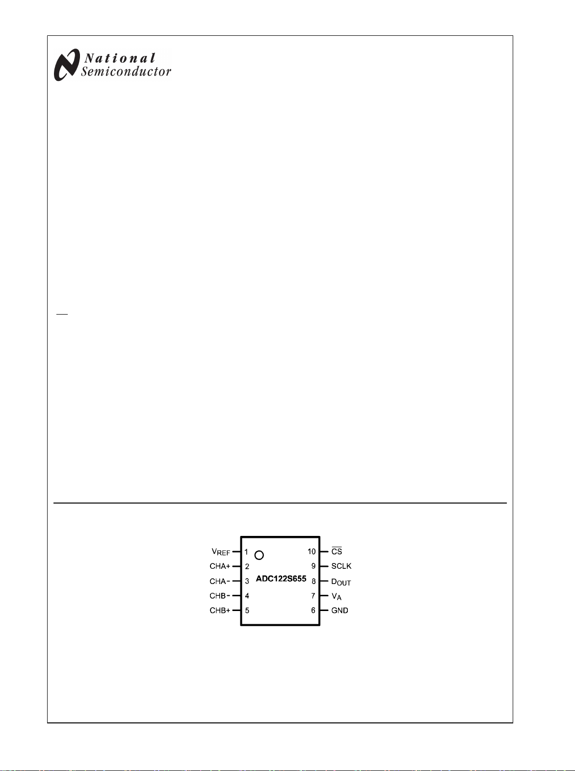
Connection Diagram
30051905
TRI-STATE® is a trademark of National Semiconductor Corporation.
MICROWIRE™ is a trademark of National Semiconductor Corporation.
QSPI™ and SPI™ are trademarks of Motorola, Inc.
© 2008 National Semiconductor Corporation 300519 www.national.com
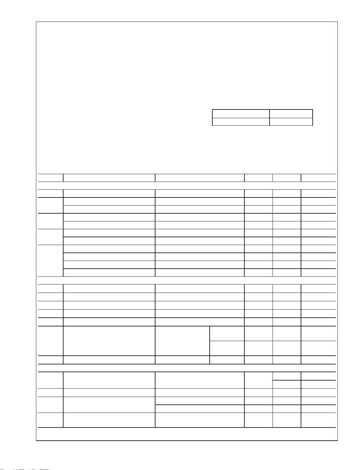
Ordering Information
Order Code Temperature Range Description Top Mark
ADC122S655CIMM −40°C to +105°C 10-Lead MSOP Package, 1000 Units Tape & Reel X96C
ADC122S655
ADC122S655CIMMX −40°C to +105°C 10-Lead MSOP Package, 3500 Units Tape & Reel X96C
ADC122S655EB Evaluation Board
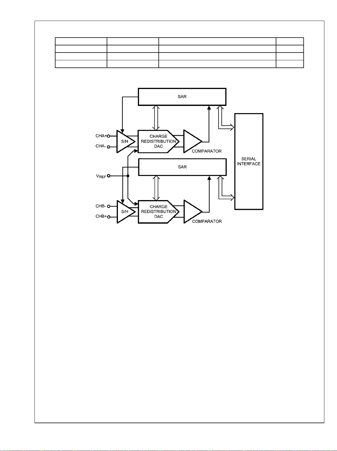
Block Diagram
30051902
www.national.com 2
Pin Descriptions and Equivalent Circuits
Pin No. Symbol Description
Voltage Reference Input. A voltage reference between 1V and VA must be applied to this
1
V
REF
input. V
µF. A bulk capacitor value of 1.0 µF to 10 µF in parallel with the 0.1 µF is recommended
for enhanced performance.
2 CHA+
3 CHA−
4 CHB−
5 CHB+
Non-Inverting Input for Channel A. CHA+ is the positive analog input for the differential
signal applied to Channel A.
Inverting Input for Channel A. CHA− is the negative analog input for the differential signal
applied to Channel A.
Inverting Input for Channel B. CHB− is the negative analog input for the differential signal
applied to Channel B.
Non-Inverting Input for Channel B. CHB+ is the positive analog input for the differential
signal applied to Channel B.
6 GND Ground. GND is the ground reference point for all signals applied to the ADC122S655.
Analog Power Supply input. A voltage source between 4.5V and 5.5V must be applied to
7
V
A
this input. VA must be decoupled to GND with a minimum ceramic capacitor value of 0.1
µF. A bulk capacitor value of 1.0 µF to 10 µF in parallel with the 0.1 µF is recommended
for enhanced performance.
Serial Data Output for Channel A and Channel B. The serial data output word is comprised
8
D
OUT
of 4 null bits, 12 data bits (ChA conversion result), 4 null bits, and 12 data bits (ChB
conversion result). During a conversion, the data is output on the falling edges of SCLK
and is valid on the rising edges.
9 SCLK Serial Clock. SCLK is used to control data transfer and serves as the conversion clock.
10 CS
Chip Select Bar. CS is active low. The ADC122S655 is actively converting when CS is
LOW and Power-Down Mode when CS is HIGH. A conversion begins on the fall of CS.
must be decoupled to GND with a minimum ceramic capacitor value of 0.1
REF
ADC122S655
3 www.national.com
Absolute Maximum Ratings (Notes 1, 2)
If Military/Aerospace specified devices are required,
please contact the National Semiconductor Sales Office/
Distributors for availability and specifications.
ADC122S655
Analog Supply Voltage V
A
Voltage on Any Pin to GND −0.3V to (VA +0.3V)
Input Current at Any Pin (Note 3) ±10 mA
Package Input Current (Note 3) ±50 mA
Power Consumption at TA = 25°C
ESD Susceptibility (Note 5)
Human Body Model
Machine Model
Charge Device Model
Junction Temperature +150°C
Storage Temperature −65°C to +150°C
−0.3V to 6.5V
See (Note 4)
2500V
250V
1000V
Operating Ratings (Notes 1, 2)
Operating Temperature Range
Supply Voltage, V
Reference Voltage, V
A
REF
Input Common-Mode Voltage, VCMSee Figure 9 (Sect 2.3)
Digital Input Pins Voltage Range 0 to V
Clock Frequency 6.4 MHz to 16 MHz
Differential Analog Input Voltage −V
−40°C ≤ TA ≤ +105°C
+4.5V to +5.5V
REF
Package Thermal Resistance
Package
10-lead MSOP 240°C / W
Soldering process must comply with National
θ
JA
Semiconductor's Reflow Temperature Profile specifications.
Refer to www.national.com/packaging. (Note 6)
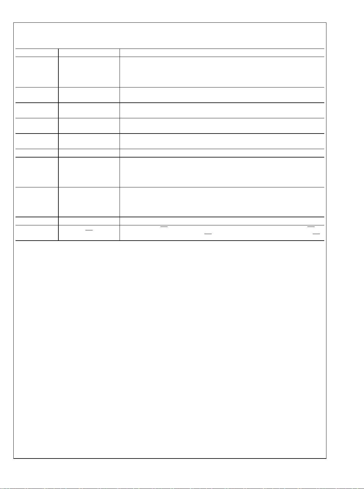
ADC122S655 Converter Electrical Characteristics (Note 7)
The following specifications apply for VA = +4.5V to 5.5V, V
otherwise noted. Boldface limits apply for TA = T
MIN
to T
Symbol Parameter Conditions Typical Limits Units
STATIC CONVERTER CHARACTERISTICS
Resolution with No Missing Codes 12 Bits
INL
DNL
OE
Integral Non-Linearity ±0.5 ±1 LSB (max)
Integral Non-Linearity Matching 0.02 LSB
Differential Non-Linearity ±0.4 ±0.95 LSB (max)
Differential Non-Linearity Matching 0.02 LSB
Offset Error 0.2 ±3 LSB (max)
Offset Error Matching 0.1 LSB
Positive Gain Error −2 ±5 LSB (max)
GE
Positive Gain Error Matching 0.2 LSB
Negative Gain Error 3 ±8 LSB (max)
Negative Gain Error Matching 0.2 LSB
DYNAMIC CONVERTER CHARACTERISTICS
SINAD Signal-to-Noise Plus Distortion Ratio
SNR Signal-to-Noise Ratio
THD Total Harmonic Distortion
SFDR Spurious-Free Dynamic Range
ENOB Effective Number of Bits
FPBW −3 dB Full Power Bandwidth
ISOL Channel-to-Channel Isolation
fIN = 100 kHz, −0.1 dBFS
fIN = 100 kHz, −0.1 dBFS
fIN = 100 kHz, −0.1 dBFS
fIN = 100 kHz, −0.1 dBFS
fIN = 100 kHz, −0.1 dBFS
Output at 70.7%FS with
FS Input
fIN < 1 MHz
ANALOG INPUT CHARACTERISTICS
V
IN
I
DCL
C
INA
CMRR Common Mode Rejection Ratio
Differential Input Range
DC Leakage Current
Input Capacitance
VIN = V
In Track Mode 20 pF
In Hold Mode 3 pF
See the Specification Definitions for the
test condition
= 2.5V, f
REF
; all other limits are at TA = 25°C.
MAX
= 6.4 to 16 MHz, fIN = 100 kHz, CL = 25 pF, unless
SCLK
Differential
Input
Single-Ended
Input
−90 dBc
or VIN = -V
REF
REF
72.5 69.5 dBc (min)
73.2 71 dBc (min)
−83 −72 dBc (max)
84 72 dBc (min)
11.8 11.25 bits (min)
26 MHz
22 MHz
−V
REF
+V
REF
±1 µA (max)
−90 dB
1.0V to V
to +V
V (min)
V (max)
A
A
REF
www.national.com 4
Symbol Parameter Conditions Typical Limits Units
V
REF
Reference Voltage Range
1.0 V (min)
V
A
V (max)
DIGITAL INPUT CHARACTERISTICS
V
IH
V
IL
I
IN
C
IND
Input High Voltage 2.4 V (min)
Input Low Voltage 0.8 V (max)
Input Current
VIN = 0V or V
A
±1 µA (max)
Input Capacitance 2 4 pF (max)
DIGITAL OUTPUT CHARACTERISTICS
V
V
I
OZH
C
OH
OL
OUT
Output High Voltage
Output Low Voltage
, I
TRI-STATE Leakage Current
OZL
TRI-STATE Output Capacitance
= 200 µA VA − 0.02
SOURCE
I
= 1 mA VA − 0.09
SOURCE
I
= 200 µA
SINK
I
= 1 mA
SINK
Force 0V or V
Force 0V or V
A
A
0.01 0.4 V (max)
0.08 V
±1 µA (max)
2 4 pF (max)
VA − 0.2
V
V (min)
I
Output Coding Binary 2'S Complement
POWER SUPPLY CHARACTERISTICS
V
A
IVA (Conv)
I
VREF
(Conv)
IVA (PD)
I
VREF
PWR
(Conv)
PWR
(PD)
Analog Supply Voltage
Analog Supply Current, Continuously
Converting
Reference Current, Continuously
Converting
Analog Supply Current, Power Down
Mode (CS high)
Reference Current, Power Down Mode
(PD)
(CS high)
Power Consumption, Continuously
Converting
Power Consumption, Power Down Mode
(CS high)
PSRR Power Supply Rejection Ratio
f
= 16 MHz, fS = 500 kSPS, fIN = 20
SCLK
kHz, VA = 5V
f
= 16 MHz, fS = 500 kSPS, V
SCLK
REF
2.5V
f
= 16 MHz, VA = 5.0V
SCLK
f
= 0, VA = 5.0V (Note 8)
SCLK
f
= 16 MHz, V
SCLK
f
= 0, V
SCLK
f
SCLK
REF
= 16 MHz, fS = 500 kSPS, fIN = 20
kHz, VA = 5.0V, V
f
= 16 MHz, VA = 5.0V, V
SCLK
f
= 0, VA = 5.0V, V
SCLK
= 2.5V
REF
= 2.5V (Note 8)
= 2.5V
REF
REF
= 2.5V
REF
= 2.5V
See the Specification Definitions for the
test condition
2.2 2.75 mA (max)
=
50 60 µA (max)
15 µA
0.5 1.1 µA (max)
0.05 µA
0.05 0.1 µA (max)
11.1 13.9 mW (max)
75 µW
2.6 5.8 µW (max)
−85 dB
4.5 V (min)
5.5 V (max)
AC ELECTRICAL CHARACTERISTICS
f
SCLK
f
SCLK
f
S
t
ACQ
t
CONV
t
AD
Maximum Clock Frequency 20 16 MHz (min)
Minimum Clock Frequency 1.6 6.4 MHz (max)
Maximum Sample Rate 625 500 kSPS (min)
Minimum Sample Rate 50 200 kSPS (min)
Track/Hold Acquisition Time 3 SCLK cycles
Conversion Time 12 SCLK cycles
Aperture Delay 6 ns
ADC122S655
5 www.national.com

ADC122S655 Timing Specifications (Note 7)
The following specifications apply for VA = +4.5V to 5.5V, V
noted. Boldface limits apply for TA = T
Symbol Parameter Conditions Typical Limits Units
ADC122S655
t
CSSU
Note 1: Absolute Maximum Ratings indicate limits beyond which damage to the device may occur. Operating Ratings indicate conditions for which the device is
functional, but do not guarantee specific performance limits. For guaranteed specifications and test conditions, see the Electrical Characteristics. The guaranteed
specifications apply only for the test conditions listed. Some performance characteristics may degrade when the device is not operated under the listed test
conditions. Operation of the device beyond the maximum Operating Ratings is not recommended.
Note 2: All voltages are measured with respect to GND = 0V, unless otherwise specified.
Note 3: When the input voltage at any pin exceeds the power supplies (that is, VIN < GND or VIN > VA), the current at that pin should be limited to 10 mA. The 50
mA maximum package input current rating limits the number of pins that can safely exceed the power supplies with an input current of 10 mA to five.
Note 4: The absolute maximum junction temperature (TJmax) for this device is 150°C. The maximum allowable power dissipation is dictated by TJmax, the
junction-to-ambient thermal resistance (θJA), and the ambient temperature (TA), and can be calculated using the formula PDMAX = (TJmax − TA)/θJA. The values
for maximum power dissipation listed above will be reached only when the ADC122S655 is operated in a severe fault condition (e.g. when input or output pins
are driven beyond the power supply voltages, or the power supply polarity is reversed). Such conditions should always be avoided.
Note 5: Human body model is a 100 pF capacitor discharged through a 1.5 kΩ resistor. Machine model is a 220 pF capacitor discharged through 0 Ω. Charge
device model simulates a pin slowly acquiring charge (such as from a device sliding down the feeder in an automated assembler) then rapidly being discharged.
Note 6: Reflow temperature profiles are different for lead-free packages.
Note 7: Tested limits are guaranteed to National's AOQL (Average Outgoing Quality Level).
Note 8: Guaranteed by design, characterization, or statistical analysis and is not tested at final test.
Note 9: While the maximum sample rate is f
Note 10: t
CS Setup Time prior to an SCLK rising edge
t
D
EN
t
DH
t
DA
t
DIS
t
CH
t
CL
t
r
t
f
Enable Time after the falling edge of CS
OUT
D
Hold time after an SCLK Falling edge
OUT
D
Access time after an SCLK Falling edge
OUT
D
Disable Time after the rising edge of CS
OUT
(Note 10)
SCLK High Time 25 ns (min)
SCLK Low Time 25 ns (min)
D
Rise Time
OUT
D
Fall Time
OUT
is the time for D
DIS
to change 10%.
OUT
to T
MIN
/32, the actual sample rate may be lower than this by having the CS rate slower than f
SCLK
: all other limits TA = 25°C.
MAX
= 2.5V, f
REF
= 6.4 MHz to 16 MHz, CL = 25 pF, unless otherwise
SCLK
4 7 ns (min)
1/ f
SCLK
1/ f
SCLK
- 3
9 20 ns (max)
9 6 ns (min)
20 26 ns (max)
10 20 ns (max)
7 ns
7 ns
/32.
SCLK
ns (max)
www.national.com 6

Timing Diagrams
ADC122S655
30051942
FIGURE 1. ADC122S655 Single Conversion Timing Diagram
FIGURE 3. D
FIGURE 4. D
FIGURE 2. ADC122S655 Continuous Conversion Timing Diagram
30051906
Rise and Fall Times
OUT
FIGURE 5. Valid CS Assertion Times
30051911
Hold and Access Times
OUT
FIGURE 6. Voltage Waveform for t
30051904
30051910
30051912
DIS
7 www.national.com

Specification Definitions
APERTURE DELAY is the time between the fourth falling
edge of SCLK and the time when the input signal is acquired
or held for conversion.
ADC122S655
COMMON MODE REJECTION RATIO (CMRR) is a measure
of how well in-phase signals common to both input pins are
rejected.
To calculate CMRR, the change in output offset is measured
while the common mode input voltage is changed from 2V to
3V.
CMRR = 20 LOG ( Δ Output Offset / Δ Common Input)
CONVERSION TIME is the time required, after the input voltage is acquired, for the ADC to convert the input voltage to a
digital word.
DIFFERENTIAL NON-LINEARITY (DNL) is the measure of
the maximum deviation from the ideal step size of 1 LSB.
DUTY CYCLE is the ratio of the time that a repetitive digital
waveform is high to the total time of one period. The specification here refers to the SCLK.
EFFECTIVE NUMBER OF BITS (ENOB, or EFFECTIVE
BITS) is another method of specifying Signal-to-Noise and
Distortion or SINAD. ENOB is defined as (SINAD − 1.76) /
6.02 and says that the converter is equivalent to a perfect
ADC of this (ENOB) number of bits.
FULL POWER BANDWIDTH is a measure of the frequency
at which the reconstructed output fundamental drops 3 dB
below its low frequency value for a full scale input.
INTEGRAL NON-LINEARITY (INL) is a measure of the deviation of each individual code from a line drawn from negative
full scale (½ LSB below the first code transition) through positive full scale (½ LSB above the last code transition). The
deviation of any given code from this straight line is measured
from the center of that code value.
MISSING CODES are those output codes that will never appear at the ADC outputs. The ADC122S655 is guaranteed not
to have any missing codes.
NEGATIVE FULL-SCALE ERROR is the difference between
the differential input voltage at which the output code transitions from negative full scale to the next code and −V
LSB.
NEGATIVE GAIN ERROR is the difference between the negative full-scale error and the offset error.
OFFSET ERROR is the difference between the differential
input voltage at which the output code transitions from code
000h to 001h and 1/2 LSB.
REF
+ 0.5
POSITIVE FULL-SCALE ERROR is the difference between
the differential input voltage at which the output code transitions to positive full scale and V
POSITIVE GAIN ERROR is the difference between the positive full-scale error and the offset error.
POWER SUPPLY REJECTION RATIO (PSRR) is a measure
of how well a change in supply voltage is rejected. PSRR is
calculated from the ratio of the change in offset error for a
given change in supply voltage, expressed in dB. For the ADC122S655, VA is changed from 4.5V to 5.5V.
PSRR = 20 LOG (ΔOffset / ΔVA)
SIGNAL TO NOISE RATIO (SNR) is the ratio, expressed in
dB, of the rms value of the input signal to the rms value of the
sum of all other spectral components below one-half the sampling frequency, not including harmonics or d.c.
SIGNAL TO NOISE PLUS DISTORTION (S/N+D or
SINAD) Is the ratio, expressed in dB, of the rms value of the
input signal to the rms value of all of the other spectral components below half the clock frequency, including harmonics
but excluding d.c.
SPURIOUS FREE DYNAMIC RANGE (SFDR) is the difference, expressed in dB, between the desired signal amplitude
to the amplitude of the peak spurious spectral component,
where a spurious spectral component is any signal present in
the output spectrum that is not present at the input and may
or may not be a harmonic.
TOTAL HARMONIC DISTORTION (THD) is the ratio of the
rms total of the first five harmonic components at the output
to the rms level of the input signal frequency as seen at the
output, expressed in dB. THD is calculated as
where Af1 is the RMS power of the input frequency at the output and Af2 through Af6 are the RMS power in the first 5
harmonic frequencies.
THROUGHPUT TIME is the minimum time required between
the start of two successive conversion.
minus 1.5 LSB.
REF
www.national.com 8

ADC122S655
Typical Performance Characteristics V
16 MHz, fIN = 100 kHz unless otherwise stated.
DNL - 500 kSPS
30051921
DNL vs. V
A
= 5.0V, V
A
= 2.5V, TA = +25°C, f
REF
INL - 500 kSPS
INL vs. V
SAMPLE
A
= 500 kSPS, f
30051922
SCLK
=
DNL vs. V
REF
30051923
30051918
30051924
INL vs. V
REF
30051919
9 www.national.com

Typical Performance Characteristics V
16 MHz, fIN = 100 kHz unless otherwise stated.
= 5.0V, V
A
= 2.5V, TA = +25°C, f
REF
SAMPLE
= 500 kSPS, f
SCLK
=
ADC122S655
DNL vs. SCLK FREQUENCY
DNL vs. TEMPERATURE
30051925
INL vs. SCLK FREQUENCY
30051926
INL vs. TEMPERATURE
30051929
SINAD vs. V
www.national.com 10
A
30051933
THD vs. V
30051930
A
30051932

ADC122S655
Typical Performance Characteristics V
16 MHz, fIN = 100 kHz unless otherwise stated.
SINAD vs. V
SINAD vs. SCLK FREQUENCY
REF
30051937
= 5.0V, V
A
= 2.5V, TA = +25°C, f
REF
THD vs. V
THD vs. SCLK FREQUENCY
SAMPLE
REF
= 500 kSPS, f
30051936
SCLK
=
SINAD vs. INPUT FREQUENCY
30051941
30051949
30051940
THD vs. INPUT FREQUENCY
30051948
11 www.national.com

Typical Performance Characteristics V
16 MHz, fIN = 100 kHz unless otherwise stated.
= 5.0V, V
A
= 2.5V, TA = +25°C, f
REF
SAMPLE
= 500 kSPS, f
SCLK
=
ADC122S655
SINAD vs. TEMPERATURE
VA CURRENT vs. V
A
30051972
THD vs. TEMPERATURE
30051971
VA CURRENT vs. SCLK FREQ
30051974
VA CURRENT vs. TEMPERATURE
30051954
www.national.com 12
V
CURRENT vs. SCLK FREQ
REF
30051955
30051952

ADC122S655
Typical Performance Characteristics V
16 MHz, fIN = 100 kHz unless otherwise stated.
V
CURRENT vs. TEMP
REF
30051951
SPECTRAL RESPONSE - 500 kSPS
= 5.0V, V
A
= 2.5V, TA = +25°C, f
REF
CMRR vs. CM RIPPLE FREQ
SAMPLE
= 500 kSPS, f
30051973
SCLK
=
30051914
13 www.national.com

Functional Description
The ADC122S655 is a dual 12-bit, simultaneous sampling
Analog-to-Digital (A/D) converter. The converter is based on
a successive-approximation register (SAR) architecture
ADC122S655
where the differential nature of the analog inputs is maintained from the internal track-and-hold circuits throughout the
A/D converter. The analog inputs on both channels are sampled simultaneously to preserve their relative phase information to each other. The architecture and process allow the
ADC122S655 to acquire and convert dual analog signals at
sample rates up to 500 kSPS while consuming very little power.
The ADC122S655 requires an external reference, external
clock, and an analog power supply. The analog supply (VA)
can range from 4.5V to 5.5V and the external reference can
be any voltage between 1V and VA. The value of the reference
voltage determines the range of the analog input, while the
reference input current depends upon the conversion rate.
Analog inputs are presented at the inputs of Channel A and
Channel B. Upon initiation of a conversion, the differential input at these pins is sampled on the internal capacitor array.
The analog input signals are disconnected from the external
circuitry while a conversion is in progress.
The external clock can take on values as indicated in the
Electrical Characteristics Table. The duty cycle of the clock is
essentially unimportant, provided the minimum clock high and
low times are met. The minimum clock frequency is set by
internal capacitor leakage. Each conversion requires thirytwo clock cycles to complete.
The ADC122S655 offers a high-speed serial data output that
is binary 2's complement and compatible with several standards, such as SPI™, QSPI™, MICROWIRE™, and many
common DSP serial interfaces. The digital conversion result
of Channel A and Channel B is clocked out on the falling
edges of the SCLK input and is provided serially at D
significant bit first. The result of Channel A is output before
the result of Channel B, with four zeros in between the two
results. The digital data provided on D
version currently in progress. With CS held low after the result
of Channel B is output, the ADC122S655 will continuously
convert the analog inputs until CS is de-asserted (brought
high). Having a single, serial D
an excellent replacement for two independent ADCs that are
OUT
part of a daisy chain configuration and allows a system designer to save valuable board space and power.
is that of the con-
OUT
makes the ADC122S655
OUT
, most
this noise can be reduced by averaging the results of a number of consecutive conversions.
Additionally, since offset and gain errors are specified in LSB,
any offset and/or gain errors inherent in the A/D converter will
increase in terms of LSB size as the reference voltage is reduced.
The reference input and the analog inputs are connected to
the capacitor array through a switch matrix when the input is
sampled. Hence, the current requirements at the reference
and at the analog inputs are a series of transient spikes that
occur at a frequency dependent on the operating sample rate
of the ADC122S655.
The reference current changes only slightly with temperature.
See the curves, “Reference Current vs. SCLK Frequency”
and “Reference Current vs. Temperature” in the Typical Performance Curves section for additional details.
2.0 ANALOG SIGNAL INPUTS
The ADC122S655 has dual differential inputs where the effective input voltage that is digitized is CHA+ minus CHA−
(DIFFINA) and CHB+ minus CHB− (DIFFINB). As is the case
with all differential input A/D converters, operation with a fully
differential input signal or voltage will provide better performance than with a single-ended input. However, the
ADC122S655 can be presented with a single-ended input as
shown in Section 2.2 and the Application Circuits.
The current required to recharge the input sampling capacitor
will cause voltage spikes at the + and − inputs. Do not try to
filter out these noise spikes. Rather, ensure that the noise
spikes settle out during the acquisition period (three SCLK
cycles after the fall of CS). This is true for both Channel A and
Channel B since both channels are converted simultaneously
on the fourth falling edge of SCLK after CS is asserted.
2.1 Differential Input Operation
With a fully differential input voltage or signal, a positive full
scale output code (0111 1111 1111b or 7FFh) will be obtained
when DIFFINA or DIFFINB is greater than or equal to V
1.5 LSB. A negative full scale code (1000 0000 0000b or
REF
800h) will be obtained when DIFFINA or DIFFINB is greater
than or equal to −V
and linearity errors, which will affect the exact differential input
+ 0.5 LSB. This ignores gain, offset
REF
voltage that will determine any given output code. Figure 7
shows the ADC122S655 being driven by a full-scale differential source.
−
1.0 REFERENCE INPUT
The externally supplied reference voltage sets the analog input range. The ADC122S655 will operate with a reference
voltage in the range of 1V to VA.
Operation with a reference voltage below 1V is also possible
with slightly diminished performance. As the reference voltage (V
voltages is reduced. Assuming a proper common-mode input
) is reduced, the range of acceptable analog input
REF
voltage, the differential peak-to-peak input range is limited to
twice V
value of V
(LSB). The size of one LSB is equal to twice the reference
. See Section 2.3 for more details. Reducing the
REF
also reduces the size of the least significant bit
REF
voltage divided by 4096. When the LSB size goes below the
noise floor of the ADC122S655, the noise will span an increasing number of codes and overall performance will suffer.
For example, dynamic signals will have their SNR degrade,
while D.C. measurements will have their code uncertainty increase. Since the noise is Gaussian in nature, the effects of
www.national.com 14
30051980
FIGURE 7. Differential Input

2.2 Single-Ended Input Operation
For single-ended operation, the non-inverting inputs of the
ADC122S655 can be driven with a signal that has a maximum
to minimum value range that is equal to or less than twice the
reference voltage. The inverting inputs should be biased at a
stable voltage that is halfway between these maximum and
minimum values. In order to utilize the entire dynamic range
of the ADC122S655, the reference voltage is limited at VA /
2. This allows the non-inverting inputs the maximum swing
range of ground to VA. Figure 8 shows the ADC122S655 being driven by a full-scale single-ended source. Even though
the design of the ADC122S655 is optimized for a differential
input, there is very little performance degradation while operating the ADC122S655 in single-ended fashion.
30051981
FIGURE 8. Single-Ended Input
2.3 Input Common Mode Voltage
The allowable input common mode voltage (VCM) range depends upon the supply and reference voltages used for the
ADC122S655. The ranges of VCM for differential and singleended operation are depicted in Figure 9 and Figure 10.
Equations for calculating the minimum and maximum common mode voltages for differential and single-ended operation are shown in Table 1.
30051961
FIGURE 9. VCM range for Differential Input operation
30051962
FIGURE 10. VCM range for single-ended operation
TABLE 1. Allowable VCM Range
Input Signal
Differential
Single-Ended
Minimum V
V
/ 2 VA − V
REF
V
REF
CM
Maximum V
REF
VA − V
REF
CM
/ 2
3.0 SERIAL DIGITAL INTERFACE
The ADC122S655 communicates via a synchronous serial
interface as shown in the Timing Diagram section. CS, chip
select, initiates conversions and frames the serial data transfers. SCLK (serial clock) controls both the conversion process
and the timing of the serial data. D
pin, where the conversion results of Channel A and Channel
is the serial data output
OUT
B are sent as a serial data stream, with the result of Channel
A output before the result of Channel B.
A serial frame is initiated on the falling edge of CS and ends
on the rising edge of CS. The ADC122S655's D
impedance state when CS is high (asserted) and is active
is in a high
OUT
when CS is low (de-asserted); thus CS acts as an output enable. A timing diagram for a single conversion is shown in
Figure 1.
During the first three cycles of SCLK, the ADC122S655 is in
acquisition mode (t
Channel A and Channel B. For the next twelve SCLK cycles
(t
), the conversion of Channel A and Channel B is ac-
CONV
complished simultaneously and data is presented on D
one bit at a time. SCLK falling edges one through four clock
), tracking the input voltage on both
ACQ
OUT
out leading zeros while falling edges five through sixteen
clock out the conversion result of Channel A, MSB first. The
process is repeated in order to clock out the result of Channel
B, with SCLK falling edges seventeen through twenty clocking
out four zeros followed by falling edges twenty-one through
thirty-two clokcing out the conversion result of Channel B. If
there is more than one conversion in a frame (continuous
conversion mode), the ADC122S655 will re-enter acquisition
mode on the falling edge of SCLK after the N*32 rising edge
of SCLK and re-enter conversion mode on the N*32+4 falling
edge of SCLK as shown in Figure 2. "N" is an integer value.
The ADC122S655 can enter acquisition mode under three
different conditions. The first condition involves CS
going low
(asserted) with SCLK high. In this case, the ADC122S655
enters acquisition mode on the first falling edge of SCLK after
CS is asserted. In the second condition, CS goes low with
SCLK low. Under this condition, the ADC122S655 automatically enters acquisition mode and the falling edge of CS is
ADC122S655
,
15 www.national.com

seen as the first falling edge of SCLK. In the third condition,
CS and SCLK go low simultaneously and the ADC122S655
immediately enters acquisition mode. While there is no timing
restriction with respect to the falling edges of CS and the
falling edge of SCLK, see Figure 5 for setup and hold time
ADC122S655
requirements for the falling edge of CS with respect to the
rising edge of SCLK.
3.1 CS
Input
(chip select bar) is an active low input that is TTL and
The CS
CMOS compatible. The ADC122S655 transitions from acquisition mode, to conversion mode, to power-down mode when
CS is low and is always in power-down mode when CS is high.
The falling edge of CS marks the beginning of a conversion
where the input to Channel A and Channel B are tracked by
the input sampling capacitor. The rising edge of CS marks the
end of a conversion window. As a result, CS frames the conversion window and can be used to control the sample rate of
the ADC122S655. While the SCLK frequency is limited to a
range of 6.4 MHz to 16 MHz, the frequency of CS has no
limitation. This allows a system designer to operate the
ADC122S655 at sample rates approaching zero samples per
second if conserving power is very important. See Burst Mode
Operation for more details. Multiple conversions can occur
within a given conversion frame with each conversion requiring thirty-two SCLK cycles. This is referred to as continuous
conversion mode and is shown in Figure 2 of the Timing Diagram section.
Proper operation requires that the fall of CS not occur simultaneously with a rising edge of SCLK. If the fall of CS occurs
during the rising edge of SCLK, the data might be clocked out
one bit early. Whether or not the data is clocked out early
depends upon how close the CS transition is to the SCLK
transition, the device temperature, and characteristics of the
individual device. To ensure that the MSB is always clocked
out at a given time (the 5th falling edge of SCLK), it is essential
that the fall of CS
always meet the timing requirement speci-
fied in the Timing Specification table.
3.2 SCLK Input
The SCLK (serial clock) serves two purposes in the
ADC122S655. It is used by the ADC122S655 as the conversion clock and it is used as the serial clock to output the
conversion results. The SCLK input is TTL and CMOS compatible. Internal settling time requirements limit the maximum
clock frequency while internal capacitor leakage limits the
minimum clock frequency. The ADC122S655 offers guaranteed performance with the clock rates indicated in the Electrical Characteristics Table.
3.3 Data Output(s)
The conversion result of Channel A and Channel B is output
on D
result of Channel B. The data output format of the
, with the result of Channel A being output before the
OUT
ADC122S655 is binary, two’s complement, as shown in Table
2. This table indicates the ideal output code for a given input
voltage and does not include the effects of offset, gain error,
linearity errors, or noise. Each data output bit is output on the
falling edges of SCLK.
TABLE 2. Ideal Output Code vs. Input Voltage
Analog Input
(+IN) − (−IN)
V
− 1.5 LSB
REF
2's
Complement
Binary Output
0111 1111 1111 7FF 2047
2's
Comp.
Hex Code
2's
Comp.
Dec Code
+ 0.5 LSB 0000 0000 0001 001 1
− 0.5 LSB 0000 0000 0000 000 0
0V − 1.5 LSB 1111 1111 1111 FFF −1
−V
+ 0.5 LSB
REF
1000 0000 0000 800 −2048
While data is output on the falling edges of SCLK, receiving
systems have the option of capturing the data from the
ADC122S655 on the subsequent rising or falling edge of
SCLK. If a receiving system is going to capture data on the
subsequent falling edges of SCLK, it is important to make sure
that the minimum hold time after an SCLK falling edge (tDH)
is acceptable. See Figure 4 for D
D
is enabled on the falling edge of CS and disabled on the
OUT
rising edge of CS. If CS is raised prior to the 16th falling edge
of SCLK, the current conversion is aborted and D
into its high impedance state. A new conversion will begin
hold and access times.
OUT
OUT
will go
when CS is taken LOW.
Applications Information
OPERATING CONDITIONS
We recommend that the following conditions be observed for
operation of the ADC122S655:
−40°C ≤ TA ≤ +105°C
+4.5V ≤ VA ≤ +5.5V
1V ≤ V
6.4 MHz ≤ f
VCM: See Section 2.3
4.0 POWER CONSUMPTION
The architecture, design, and fabrication process allow the
ADC122S655 to operate at conversion rates up to 500 kSPS
while consuming very little power. The ADC122S655 consumes the least amount of power while operating in power
down mode. For applications where power consumption is
critical, the ADC122S655 should be operated in power down
mode as often as the application will tolerate. To further reduce power consumption, stop the SCLK while CS is high.
4.1 Burst Mode Operation
Normal operation of the ADC122S655 requires the SCLK frequency to be thirty-two times the sample rate and the CS rate
to be the same as the sample rate. However, in order to minimize power consumption in applications requiring sample
rates below 200 kSPS, the ADC122S655 should be run with
an SCLK frequency of 16 MHz and a CS rate as slow as the
system requires. When this is accomplished, the
ADC122S655 is operating in burst mode. The ADC122S655
enters into power down mode at the end of each conversion,
minimizing power consumption. This causes the converter to
spend the longest possible time in power down mode. Since
power consumption scales directly with conversion rate, minimizing power consumption requires determining the lowest
conversion rate that will satisfy the requirements of the system.
REF
≤ V
SCLK
A
≤ 16 MHz
www.national.com 16

ADC122S655
5.0 POWER SUPPLY CONSIDERATIONS AND PCB LAYOUT
For best performance, care should be taken with the physical
layout of the printed circuit board. This is especially true with
a low reference voltage or when the conversion rate is high.
At high clock rates there is less time for settling, so it is important that any noise settles out before the conversion begins.
5.1 Analog Power Supply
Any ADC architecture is sensitive to spikes on the power supply, reference, and ground pins. These spikes may originate
from switching power supplies, digital logic, high power devices, and other sources. Power to the ADC122S655 should
be clean and well bypassed. A 0.1 µF ceramic bypass capacitor and a 1 µF to 10 µF capacitor should be used to
bypass the ADC122S655 supply, with the 0.1 µF capacitor
placed as close to the ADC122S655 package as possible.
Since the ADC122S655 has a separate analog and reference
pin, the user has two options. The first option is to tie the analog and reference supply pins together and power them with
the same power supply. This is the most cost effective way of
powering the ADC122S655 but it is also the least ideal. As
stated previously, noise from the analog supply pin can couple into the reference supply pin and adversely affect performance. The other option involves the user powering the
analog and reference supply pins with separate supply voltages. These supply voltages can have the same amplitude or
they can be different. The only design constraint is that the
reference supply voltage be less than the analog supply voltage.
should be isolated from noisy signal traces to avoid coupling
of spurious signals into the input. Any external component
(e.g., a filter capacitor) connected between the converter's
input pins and ground or to the reference input pin and ground
should be connected to a very clean point in the ground plane.
A single, uniform ground plane and the use of split power
planes are recommended. The power planes should be located within the same board layer. All analog circuitry (input
amplifiers, filters, reference components, etc.) should be
placed over the analog power plane. All digital circuitry and
I/O lines should be placed over the digital power plane. Furthermore, the GND pin on the ADC122S655 and all the
components in the reference circuitry and input signal chain
that are connected to ground should be connected to the
ground plane at a quiet point. Avoid connecting these points
too close to the ground point of a microprocessor, microcontroller, digital signal processor, or other high power digital
device.
6.0 APPLICATION CIRCUITS
The following figures are examples of the ADC122S655 in
typical application circuits. These circuits are basic and will
generally require modification for specific circumstances.
6.1 Data Acquisition
Figure 11 shows a basic low cost, low power data acquisition
circuit. The analog supply pin is powered by the system +5V
supply and the 2.5V reference voltage is generated by the
LM4040-2.5 shunt reference.
5.2 Voltage Reference
The reference source must have a low output impedance and
needs to be bypassed with a minimum capacitor value of 0.1
µF. A larger capacitor value of 1 µF to 10 µF placed in parallel
with the 0.1 µF is preferred. While the ADC122S655 draws
very little current from the reference on average, there are
higher instantaneous current spikes at the reference input.
The reference input of the ADC122S655, like all A/D converters, does not reject noise or voltage variations. Keep this in
mind if the reference voltage is derived from the power supply.
Any noise and/or ripple from the supply that is not rejected by
the external reference circuitry will appear in the digital results. The use of an active reference source is recommended.
The LM4040 and LM4050 shunt reference families and the
LM4132 and LM4140 series reference families are excellent
choices for a reference source.
5.3 PCB Layout
Capacitive coupling between the noisy digital circuitry and the
sensitive analog circuitry can lead to poor performance. The
solution is to keep the analog circuitry separated from the
digital circuitry and the clock line as short as possible. Digital
circuits create substantial supply and ground current transients. The logic noise generated could have significant impact upon system noise performance. To avoid performance
degradation of the ADC122S655 due to supply noise, avoid
sharing the power supplies for VA and V
circuity on the board.
with other digital
REF
Generally, analog and digital lines should cross each other at
90° to avoid crosstalk. However, to maximize accuracy in high
resolution systems, avoid crossing analog and digital lines altogether. It is important to keep clock lines as short as possible and isolated from other lines, including other digital lines.
In addition, the clock line should also be treated as a transmission line and be properly terminated. The analog input
30051934
FIGURE 11. Low cost, low power Data Acquisition
System
6.2 Current Sensing Application
Figure 12 shows an example of interfacing a pair of current
transducers to the ADC122S655. The current transducers
convert an input current into a voltage that is converted by the
ADC122S655. Since the output voltage of the current transducers are single-ended and centered around a commonmode voltage of 2.5V, the ADC122S655 is configured with the
output of the transducer driving the non-inverting inputs and
the common-mode output voltage of the transducer driving
the inverting input. The output of the transducer has an output
range of ±2V around the common-mode voltage of 2.5V. As
a result, a series reference voltage of 2.0V is connected to the
ADC122S655. This will allow all of the codes of the
ADC122S655 to be available for the application. This configuration of the ADC122S655 is referred to as a single-ended
application of a differential ADC. All of the elements in the
17 www.national.com

application are conveniently powered by the same +5V power
supply, keeping circuit complexity and cost to a minimum.
ADC122S655
FIGURE 12. Interfacing the ADC122S655 to a Current Transducer
30051938
6.3 Bridge Sensor Application
Figure 13 shows an example of interfacing the ADC122S655
to a pair of bridge sensors. The application assumes that the
bridge sensors require buffering and amplification to fully utilize the dynamic range of the ADC and thus optimize the
performance of the entire signal path. The amplification stage
for each ADC input consists of a pair of opamps from the
LMP7704. The amplification stage offers the benefit of high
input impedance and potentially high amplification. On the
other hand, it offers no common-mode rejection of noise coming from the bridge sensors. The application circuit assumes
the bridge sensors are powered from the same +5V power
supply voltage as the analog supply pin on the ADC122S655.
This has the benefit of providing the ideal common-mode input voltage for the ADC122S655 while keeping design complexity and cost to a minimum. The LM4132-4.1, a 4.1V series
reference, is used as the reference voltage in the application.
FIGURE 13. Interfacing the ADC122S655 to Bridge Sensors
www.national.com 18
30051935

Physical Dimensions inches (millimeters) unless otherwise noted
ADC122S655
Order Number ADC122S655CIMM
10-Lead MSOP
NS Package Number MUB10A
19 www.national.com

Notes
For more National Semiconductor product information and proven design tools, visit the following Web sites at:
Products Design Support
Amplifiers www.national.com/amplifiers WEBENCH www.national.com/webench
Audio www.national.com/audio Analog University www.national.com/AU
Clock Conditioners www.national.com/timing App Notes www.national.com/appnotes
Data Converters www.national.com/adc Distributors www.national.com/contacts
Displays www.national.com/displays Green Compliance www.national.com/quality/green
Ethernet www.national.com/ethernet Packaging www.national.com/packaging
Interface www.national.com/interface Quality and Reliability www.national.com/quality
LVDS www.national.com/lvds Reference Designs www.national.com/refdesigns
Power Management www.national.com/power Feedback www.national.com/feedback
Switching Regulators www.national.com/switchers
LDOs www.national.com/ldo
LED Lighting www.national.com/led
PowerWise www.national.com/powerwise
Serial Digital Interface (SDI) www.national.com/sdi
Temperature Sensors www.national.com/tempsensors
Wireless (PLL/VCO) www.national.com/wireless
THE CONTENTS OF THIS DOCUMENT ARE PROVIDED IN CONNECTION WITH NATIONAL SEMICONDUCTOR CORPORATION
(“NATIONAL”) PRODUCTS. NATIONAL MAKES NO REPRESENTATIONS OR WARRANTIES WITH RESPECT TO THE ACCURACY
OR COMPLETENESS OF THE CONTENTS OF THIS PUBLICATION AND RESERVES THE RIGHT TO MAKE CHANGES TO
SPECIFICATIONS AND PRODUCT DESCRIPTIONS AT ANY TIME WITHOUT NOTICE. NO LICENSE, WHETHER EXPRESS,
IMPLIED, ARISING BY ESTOPPEL OR OTHERWISE, TO ANY INTELLECTUAL PROPERTY RIGHTS IS GRANTED BY THIS
DOCUMENT.
TESTING AND OTHER QUALITY CONTROLS ARE USED TO THE EXTENT NATIONAL DEEMS NECESSARY TO SUPPORT
NATIONAL’S PRODUCT WARRANTY. EXCEPT WHERE MANDATED BY GOVERNMENT REQUIREMENTS, TESTING OF ALL
PARAMETERS OF EACH PRODUCT IS NOT NECESSARILY PERFORMED. NATIONAL ASSUMES NO LIABILITY FOR
APPLICATIONS ASSISTANCE OR BUYER PRODUCT DESIGN. BUYERS ARE RESPONSIBLE FOR THEIR PRODUCTS AND
APPLICATIONS USING NATIONAL COMPONENTS. PRIOR TO USING OR DISTRIBUTING ANY PRODUCTS THAT INCLUDE
NATIONAL COMPONENTS, BUYERS SHOULD PROVIDE ADEQUATE DESIGN, TESTING AND OPERATING SAFEGUARDS.
EXCEPT AS PROVIDED IN NATIONAL’S TERMS AND CONDITIONS OF SALE FOR SUCH PRODUCTS, NATIONAL ASSUMES NO
LIABILITY WHATSOEVER, AND NATIONAL DISCLAIMS ANY EXPRESS OR IMPLIED WARRANTY RELATING TO THE SALE
AND/OR USE OF NATIONAL PRODUCTS INCLUDING LIABILITY OR WARRANTIES RELATING TO FITNESS FOR A PARTICULAR
PURPOSE, MERCHANTABILITY, OR INFRINGEMENT OF ANY PATENT, COPYRIGHT OR OTHER INTELLECTUAL PROPERTY
RIGHT.
LIFE SUPPORT POLICY
NATIONAL’S PRODUCTS ARE NOT AUTHORIZED FOR USE AS CRITICAL COMPONENTS IN LIFE SUPPORT DEVICES OR
SYSTEMS WITHOUT THE EXPRESS PRIOR WRITTEN APPROVAL OF THE CHIEF EXECUTIVE OFFICER AND GENERAL
COUNSEL OF NATIONAL SEMICONDUCTOR CORPORATION. As used herein:
Life support devices or systems are devices which (a) are intended for surgical implant into the body, or (b) support or sustain life and
whose failure to perform when properly used in accordance with instructions for use provided in the labeling can be reasonably expected
to result in a significant injury to the user. A critical component is any component in a life support device or system whose failure to perform
can be reasonably expected to cause the failure of the life support device or system or to affect its safety or effectiveness.
National Semiconductor and the National Semiconductor logo are registered trademarks of National Semiconductor Corporation. All other
brand or product names may be trademarks or registered trademarks of their respective holders.
Copyright© 2008 National Semiconductor Corporation
For the most current product information visit us at www.national.com
ADC122S655 Dual 12-Bit, 200 kSPS to 500 kSPS, Simultaneous Sampling A/D Converter
www.national.com
National Semiconductor
Americas Technical
Support Center
Email:
new.feedback@nsc.com
Tel: 1-800-272-9959
National Semiconductor Europe
Technical Support Center
Email: europe.support@nsc.com
German Tel: +49 (0) 180 5010 771
English Tel: +44 (0) 870 850 4288
National Semiconductor Asia
Pacific Technical Support Center
Email: ap.support@nsc.com
National Semiconductor Japan
Technical Support Center
Email: jpn.feedback@nsc.com
 Loading...