

查询ADC081S101CIMF供应商
ADC121S101/ADC101S101/ADC081S101
1MSPS, 12-/10-/8-Bit A/D Converters in SOT-23 & LLP
ADC121S101/ADC101S101/ADC081S101 1MSPS, 12-/10-/8-Bit A/D Converters in SOT-23 & LLP
January 2005
General Description
The ADC121S101, ADC101S101, and ADC081S101 are low
power, monolithic CMOS 12-, 10- and 8-bit analog-to-digital
converters that operate at 1 MSPS. Each device is based on
a successive approximation register architecture with internal track-and-hold. The serial interface is compatible with
several standards, such as SPI
and many common DSP serial interfaces.
The ADC121S101/101S101/081S101 uses the supply voltage as a reference. This enables the devices to operate with
a full-scale input range of 0 to V
determined from the serial clock (SCLK) speed. These converters offer a shutdown mode, which can be used to trade
throughput for power consumption. The ADC121S101/
101S101/081S101 are operated with a single supply that
can range from +2.7V to +5.25V. Normal power consumption
during continuous conversion, using a +3V or +5V supply, is
2 mW or 10 mW, respectively. The power down feature,
which is enabled by a chip select (CS) pin, reduces the
power consumption to under 5 µW using a +5V supply. All
three converters are available in a 6-lead SOT-23 package,
which provides an extremely small footprint for applications
where space is a critical consideration. The ADC081S101 is
also available in a 6-lead LLP package. These products are
designed for operation over the industrial temperature range
of −40˚C to +85˚C, with some parameters specified to
+125˚C for the ADC121S101.
™
, QSPI™, MICROWIRE™,
. The conversion rate is
DD
Features
n Variable power management
n Packaged in 6-lead SOT-23 (ADC081S101 also
available in a 6-Lead LLP package)
n Power supply used as reference
n Single +2.7V to +5.25V supply operation
™
n SPI
/QSPI™/MICROWIRE™/DSP compatible
Key Specifications
n Resolution with no Missing Codes 12/10/8 bits
n Conversion Rate 1 MSPS
n DNL (ADC121S101) +0.5, -0.3 LSB (typ)
n INL (ADC121S101)
n Power Consumption
— 3V Supply 2 mW (typ)
— 5V Supply 10 mW (typ)
±
0.4 LSB (typ)
Applications
n Automotive Navigation
n FA/ATM Equipment
n Portable Systems
n Medical Instruments
n Mobile Communications
n Instrumentation and Control Systems
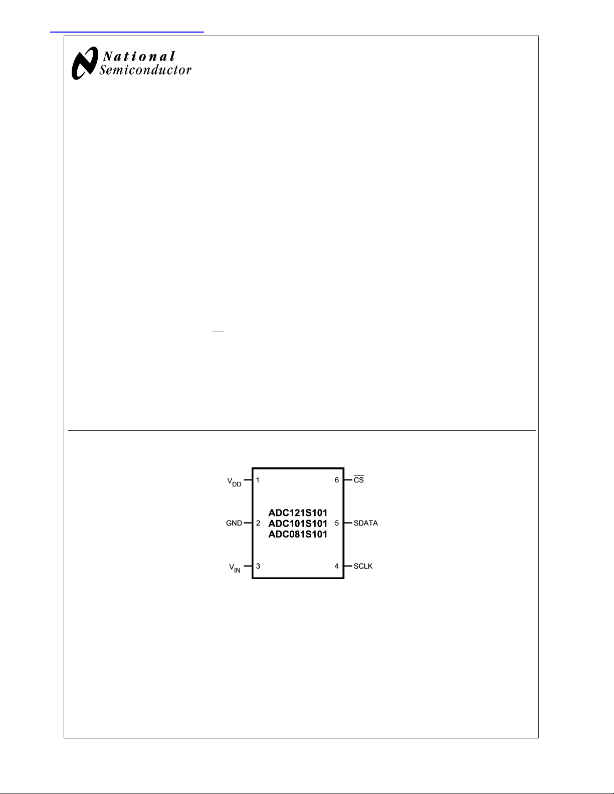
Connection Diagram
MICROWIRE™is a trademark of National Semiconductor Corporation.
®
TRI-STATE
QSPI
is a trademark of National Semiconductor Corporation.
™
and SPI™are trademarks of Motorola, Inc.
20110201
© 2005 National Semiconductor Corporation DS201102 www.national.com
Ordering Information
Order Code Temperature
Range
ADC121S101CIMF −40˚C to
+125˚C
ADC101S101CIMF −40˚C to +85˚C 6-Lead SOT-23 Package X02C
ADC081S101CIMF −40˚C to +85˚C 6-Lead SOT-23 Package X03C
ADC121S101CIMFX −40˚C to
+125˚C
ADC101S101CIMFX −40˚C to +85˚C 6-Lead SOT-23 Package, Tape & Reel X02C
ADC081S101CIMFX −40˚C to +85˚C 6-Lead SOT-23 Package, Tape & Reel X03C
ADC081S101CISDX −40˚C to +85˚C 6-Lead LLP Package, Tape & Reel X3C
ADC081S101CISD −40˚C to +85˚C 6-Lead LLP Package, Tape & Partial Reel X3C
ADC121S101/ADC101S101/ADC081S101
ADC121S101EVAL SOT-23 Evaluation Board
ADC101S101EVAL SOT-23 Evaluation Board
ADC081S101EVAL SOT-23 Evaluation Board
6-Lead SOT-23 Package, Tape & Reel X01C
Description Top Mark
6-Lead SOT-23 Package X01C
Pin Descriptions
Pin No. Symbol Description
ANALOG I/O
3V
DIGITAL I/O
4 SCLK
5 SDATA Digital data output. The output words are clocked out of this pin by the SCLK pin.
6CS
POWER SUPPLY
1V
2 GND The ground return for the supply.
IN
DD
Analog input. This signal can range from 0V to VDD.
Digital clock input. The range of frequencies for this input is 10 kHz to 20 MHz, with
guaranteed performance at 20 MHz. This clock directly controls the conversion and readout
processes.
Chip select. A conversion process begins on the falling edge of CS.
Positive supply pin. These pins should be connected to a quiet +2.7V to +5.25V source and
bypassed to GND with 0.1 µF and 1 µF monolithic capacitors located within 1 cm of the
power pin. The ADC121S101/101S101/081S101 uses this power supply as a reference, so it
should be thoroughly bypassed.
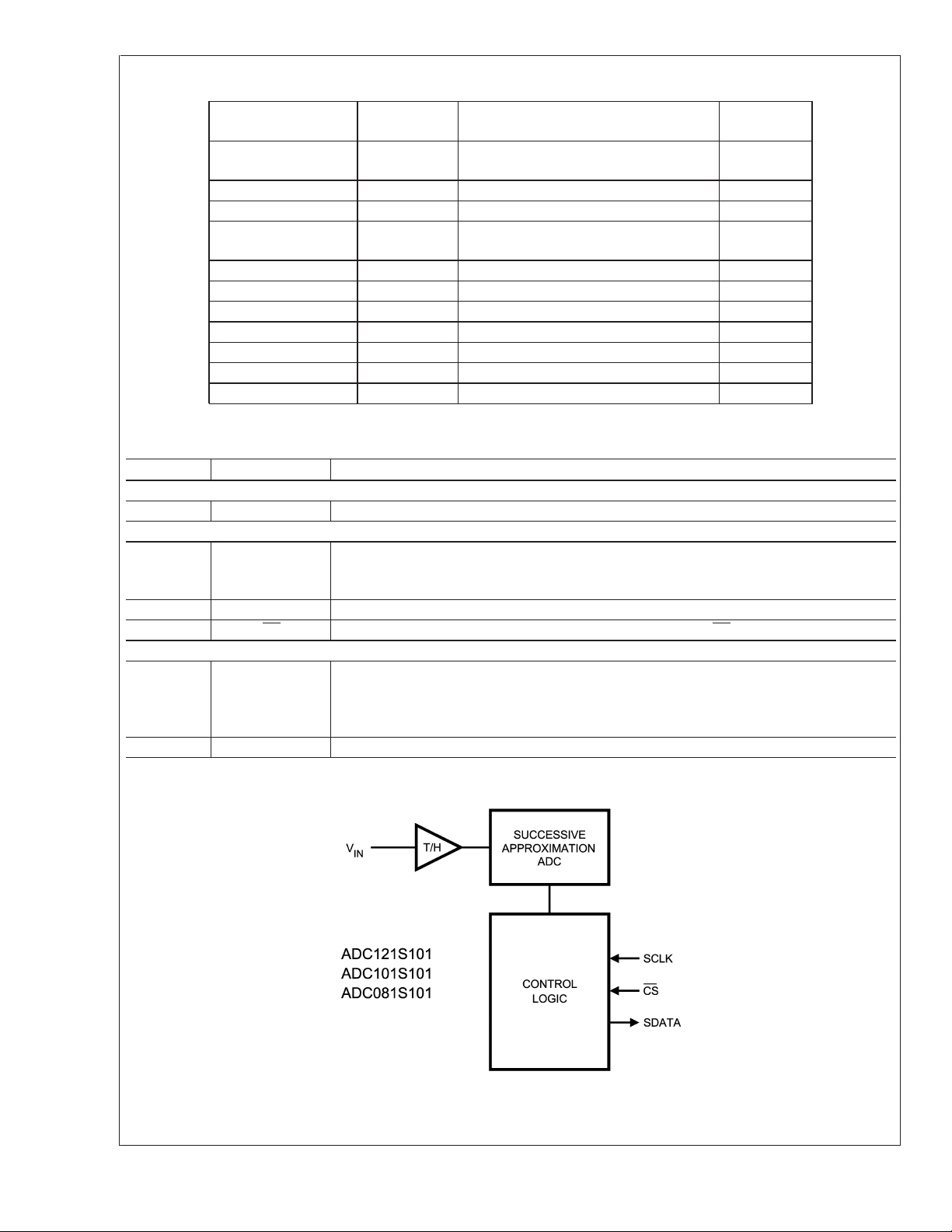
Block Diagram
www.national.com 2
20110218
ADC121S101/ADC101S101/ADC081S101
Absolute Maximum Ratings
(Notes 1, 2)
If Military/Aerospace specified devices are required,
please contact the National Semiconductor Sales Office/
Distributors for availability and specifications.
Supply Voltage V
DD
Voltage on Any Analog Pin to GND −0.3V to V
−0.3V to +6.5V
+0.3V
DD
Operating Ratings (Note 2)
Operating Temperature Range
ADC121S101
ADC101S101 & ADC081S101
V
Supply Voltage +2.7V to +5.25V
DD
−40˚C ≤ T
−40˚C ≤ T
Digital Input Pins Voltage Range
(Note 6) +2.7V to +5.25V
≤ +125˚C
A
≤ +85˚C
A
Voltage on Any Digital Pin to GND -0.3V to 6.5V
Input Current at Any Pin (Note 5)
ESD Susceptibility
Human Body Model
Machine Model
Soldering Temperature, Infrared,
±
10 mA
3500V
200V
Package Thermal Resistance
Package θ
6-Lead SOT-23 265˚C / W
6-Lead LLP 94˚C / W
JA
10 seconds 215˚C
Junction Temperature +150˚C
Storage Temperature −65˚C to +150˚C
Soldering process must comply with National
Semiconductor’s Reflow Temperature Profile
specifications. Refer to www.national.com/packaging.
(Note 4)
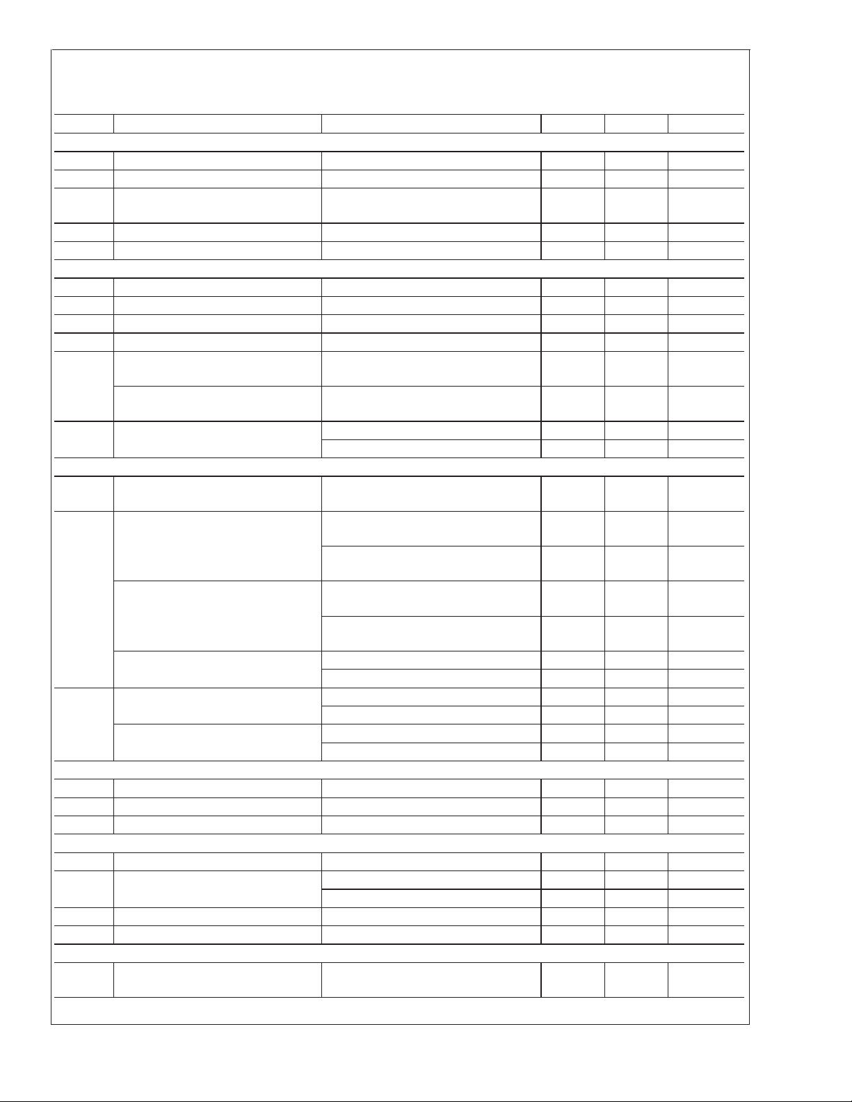
ADC121S101 Converter Electrical Characteristics
The following specifications apply for VDD= +2.7V to 5.25V, f
face limits apply for T
= −40˚C to +85˚C: all other limits TA= 25˚C, unless otherwise noted.
A
Symbol Parameter Conditions Typical Limits Units
STATIC CONVERTER CHARACTERISTICS (V
= 2.7V to 3.6V)
DD
Resolution with No Missing Codes −40˚C ≤ T
−40˚C ≤ T
INL Integral Non-Linearity
DNL Differential Non-Linearity
V
OFF
Offset Error −40˚C ≤ TA≤ 125˚C
T
= 125˚C
A
−40˚C ≤ TA≤ 85˚C
T
= 125˚C
A
GE Gain Error −40˚C ≤ T
DYNAMIC CONVERTER CHARACTERISTICS (f
= 100 kHz, -0.02 dBFS sine wave unless otherwise noted)
IN
SINAD Signal-to-Noise Plus Distortion Ratio −40˚C ≤ T
SNR Signal-to-Noise Ratio
−40˚C ≤ T
T
= 125˚C 70.6 dB (min)
A
THD Total Harmonic Distortion -80 dB
SFDR Spurious-Free Dynamic Range 82 dB
Intermodulation Distortion, Second
IMD
Order Terms
Intermodulation Distortion, Third
Order Terms
FPBW -3 dB Full Power Bandwidth
f
= 103.5 kHz, fb= 113.5 kHz -78 dB
a
= 103.5 kHz, fb= 113.5 kHz -78 dB
f
a
+5V Supply 11 MHz
+3V Supply 8 MHz
POWER SUPPLY CHARACTERISTICS
V
DD
Supply Voltage −40˚C ≤ TA≤ 125˚C
= 20 MHz, f
SCLK
≤ 125˚C 12 Bits
A
≤ 85˚C
A
≤ 125˚C
A
≤ 125˚C 72 70 dB (min)
A
≤ 85˚C 72.5 70.8 dB (min)
A
= 1 MSPS unless otherwise noted. Bold-
SAMPLE
±
0.4
±
1 LSB (max)
+1
-1.1
+0.5
-0.3
±
0.1
±
0.2
+1
-0.9
±
1 LSB (max)
±
1.2 LSB (max)
±
1.2 LSB (max)
LSB (min)
LSB (max)
LSB (max)
LSB (min)
2.7 V (min)
5.25 V (max)
www.national.com3
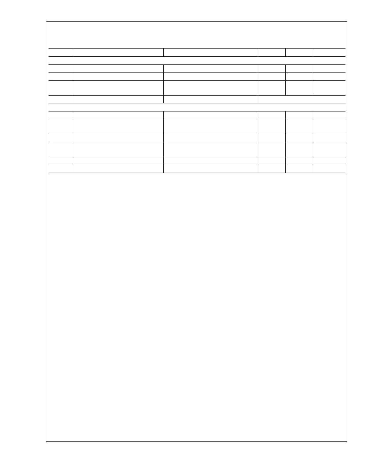
ADC121S101 Converter Electrical Characteristics (Continued)
The following specifications apply for VDD= +2.7V to 5.25V, f
face limits apply for T
= −40˚C to +85˚C: all other limits TA= 25˚C, unless otherwise noted.
A
Symbol Parameter Conditions Typical Limits Units
POWER SUPPLY CHARACTERISTICS
V
= +4.75V to +5.25V,
DD
Normal Mode (Static)
SCLK On or Off
= +2.7V to +3.6V,
V
DD
SCLK On or Off
I
DD
Normal Mode (Operational)
ADC121S101/ADC101S101/ADC081S101
Shutdown Mode
Power Consumption, Normal Mode
P
D
(Operational)
Power Consumption, Shutdown Mode
VDD= +4.75V to +5.25V,
f
V
f
V
V
V
V
V
V
= 1 MSPS
SAMPLE
= +2.7V to +3.6V,
DD
= 1 MSPS
SAMPLE
= +5V, SCLK Off 0.5 µA
DD
= +5V, SCLK On 60 µA
DD
= +5V, f
DD
= +3V, f
DD
= +5V, SCLK Off 2.5 µW
DD
= +3V, SCLK Off 1.5 µW
DD
ANALOG INPUT CHARACTERISTICS
V
I
C
IN
DCL
INA
Input Range 0 to V
DC Leakage Current
Input Capacitance (Note 3) 30 pF
DIGITAL INPUT CHARACTERISTICS
V
IH
V
IL
I
IN
C
IND
Input High Voltage 2.4 V (min)
= +5V 0.8 V (max)
V
Input Low Voltage
DD
V
= +3V 0.4 V (max)
DD
Input Current VIN=0VorV
Input Capacitance (Note 3) 2 4 pF (max)
DIGITAL OUTPUT CHARACTERISTICS
I
V
OH
V
OL
I
OL
C
OUT
Output High Voltage
Output Low Voltage I
TRI-STATE Leakage Current
TRI-STATE Output Capacitance 2 4 pF (max)
SOURCE
V
SINK
= 200 µA,
= +2.7V to +5.25V
DD
= 200 µA 0.4 V (max)
Output Coding Straight (Natural) Binary
AC ELECTRICAL CHARACTERISTICS
f
SCLK
Clock Frequency 20 MHz (max)
DC SCLK Duty Cycle
t
TH
f
RATE
t
AD
t
AJ
Track/Hold Acquisition Time 400 ns (max)
Throughput Rate See Serial Interface Section 1
Aperture Delay 3 ns
Aperture Jitter 30 ps
SCLK
SAMPLE
SAMPLE
DD
= 20 MHz, f
= 1 MSPS unless otherwise noted. Bold-
SAMPLE
2mA
1mA
2.0 3.2 mA (max)
0.6 1.5 mA (max)
= 1 MSPS 10 16 mW (max)
= 1 MSPS 2 4.5 mW (max)
DD
±
1 µA (max)
±
10 nA
±
1 µA (max)
V
−0.2 V (min)
DD
±
10 µA (max)
40
60
V
% (min)
% (max)
MSPS
(max)
www.national.com 4
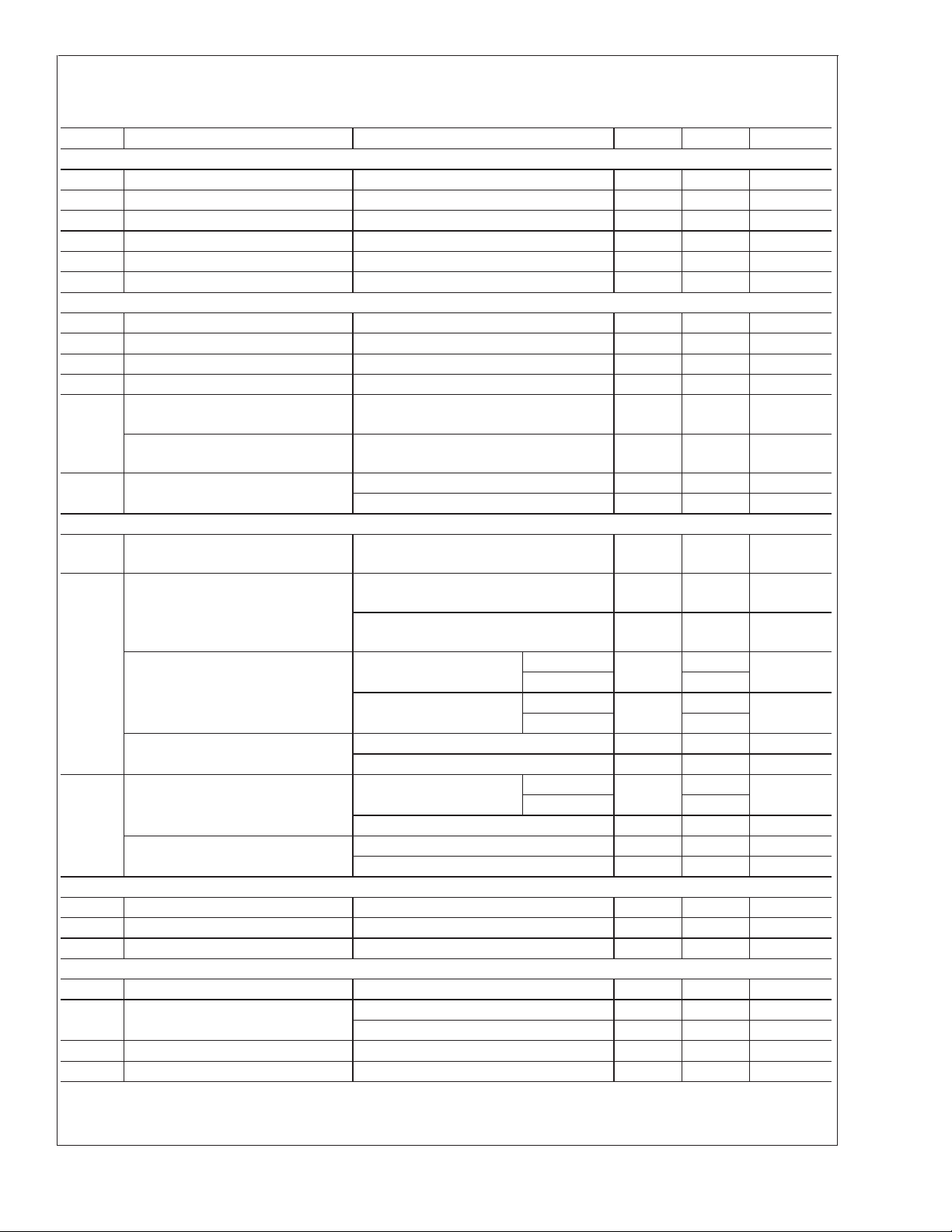
ADC101S101 Converter Electrical Characteristics
The following specifications apply for VDD= +2.7V to 5.25V, f
face limits apply for T
= −40˚C to +85˚C: all other limits TA= 25˚C, unless otherwise noted.
A
Symbol Parameter Conditions Typical Limits Units
STATIC CONVERTER CHARACTERISTICS
Resolution with No Missing Codes 10 Bits
INL Integral Non-Linearity
DNL Differential Non-Linearity
V
OFF
Offset Error
GE Gain Error
DYNAMIC CONVERTER CHARACTERISTICS
SINAD Signal-to-Noise Plus Distortion Ratio f
SNR Signal-to-Noise Ratio f
THD Total Harmonic Distortion f
SFDR Spurious-Free Dynamic Range f
Intermodulation Distortion, Second
IMD
Order Terms
Intermodulation Distortion, Third
Order Terms
FPBW -3 dB Full Power Bandwidth
= 100 kHz 61.7 61 dBFS (min)
IN
= 100 kHz 62 dB
IN
= 100 kHz -77 -73 dB (max)
IN
= 100 kHz 78 74 dB (min)
IN
f
= 103.5 kHz, fb= 113.5 kHz -78 dB
a
fa= 103.5 kHz, fb= 113.5 kHz -78 dB
+5V Supply 11 MHz
+3V Supply 8 MHz
POWER SUPPLY CHARACTERISTICS
V
DD
Supply Voltage
Normal Mode (Static)
V
= +4.75V to +5.25V,
DD
SCLK On or Off
= +2.7V to +3.6V,
V
DD
SCLK On or Off
I
DD
Normal Mode (Operational)
Shutdown Mode
Power Consumption, Normal Mode
P
D
(Operational)
Power Consumption, Shutdown Mode
VDD= +4.75V to +5.25V,
f
V
f
V
V
V
V
V
V
= 1 MSPS
SAMPLE
= +2.7V to +3.6V,
DD
= 1 MSPS
SAMPLE
= +5V, SCLK Off 0.5 µA (max)
DD
= +5V, SCLK On 60 µA (max)
DD
= +5V, f
DD
= +3V, f
DD
= +5V, SCLK Off 2.5 µW (max)
DD
= +3V, SCLK Off 1.5 µW (max)
DD
ANALOG INPUT CHARACTERISTICS
V
I
C
IN
DCL
INA
Input Range 0 to V
DC Leakage Current
Input Capacitance (Note 3) 30 pF
DIGITAL INPUT CHARACTERISTICS
V
IH
V
IL
I
IN
C
IND
Input High Voltage 2.4 V (min)
= +5V 0.8 V (max)
V
Input Low Voltage
DD
V
= +3V 0.4 V (max)
DD
Input Current VIN=0VorV
Input Capacitance (Note 3) 2 4 pF (max)
DIGITAL OUTPUT CHARACTERISTICS
I
V
OH
Output High Voltage
SOURCE
V
= 200 µA,
= +2.7V to +5.25V
DD
SCLK
SAMPLE
SAMPLE
DD
= 20 MHz, f
= 1 MSPS unless otherwise noted. Bold-
SAMPLE
±
0.2
+0.3
-0.2
±
0.1
±
0.2
±
0.7 LSB (max)
±
0.7
±
0.7 LSB (max)
±
1 LSB (max)
2.7
5.25
LSB (max)
LSB (max)
V (min)
V (max)
2mA
1mA
2.0 3.2 mA (max)
0.6 1.5 mA (max)
= 1 MSPS 10 16 mW (max)
= 1 MSPS 2 4.5 mW (max)
DD
±
1 µA (max)
±
10 nA
±
1 µA (max)
V
−0.2 V (min)
DD
ADC121S101/ADC101S101/ADC081S101
V
www.national.com5
ADC101S101 Converter Electrical Characteristics (Continued)
The following specifications apply for VDD= +2.7V to 5.25V, f
face limits apply for T
= −40˚C to +85˚C: all other limits TA= 25˚C, unless otherwise noted.
A
Symbol Parameter Conditions Typical Limits Units
DIGITAL OUTPUT CHARACTERISTICS
V
OL
I
OL
C
OUT
Output Low Voltage I
TRI-STATE Leakage Current
TRI-STATE Output Capacitance
(Note 3)
= 200 µA 0.4 V (max)
SINK
Output Coding Straight (Natural) Binary
AC ELECTRICAL CHARACTERISTICS
f
SCLK
Clock Frequency 20 MHz (max)
DC SCLK Duty Cycle
ADC121S101/ADC101S101/ADC081S101
t
TH
f
RATE
t
AD
t
AJ
Track/Hold Acquisition Time 400 ns (max)
Throughput Rate See Serial Interface Section 1
Aperture Delay 3 ns
Aperture Jitter 30 ps
SCLK
= 20 MHz, f
= 1 MSPS unless otherwise noted. Bold-
SAMPLE
±
10 µA (max)
2 4 pF (max)
40
60
% (min)
% (max)
MSPS
(max)
www.national.com 6
ADC081S101 Converter Electrical Characteristics
The following specifications apply for VDD= +2.7V to 5.25V, f
face limits apply for T
= −40˚C to +85˚C: all other limits TA= 25˚C, unless otherwise noted.
A
Symbol Parameter Conditions Typical Limits Units
STATIC CONVERTER CHARACTERISTICS
Resolution with No Missing Codes 8 Bits
INL Integral Non-Linearity
DNL Differential Non-Linearity
V
OFF
Offset Error
GE Gain Error
Total Unadjusted Error
DYNAMIC CONVERTER CHARACTERISTICS
SINAD Signal-to-Noise Plus Distortion Ratio f
SNR Signal-to-Noise Ratio f
THD Total Harmonic Distortion f
SFDR Spurious-Free Dynamic Range f
Intermodulation Distortion, Second
IMD
Order Terms
Intermodulation Distortion, Third
Order Terms
FPBW -3 dB Full Power Bandwidth
= 100 kHz 49.7 49 dB (min)
IN
= 100 kHz 49.7 dB
IN
= 100 kHz -77 -65 dB (max)
IN
= 100 kHz 69 65 dB (min)
IN
f
= 103.5 kHz, fb= 113.5 kHz -68 dB
a
fa= 103.5 kHz, fb= 113.5 kHz -68 dB
+5V Supply 11 MHz
+3V Supply 8 MHz
POWER SUPPLY CHARACTERISTICS
V
DD
Supply Voltage
Normal Mode (Static)
V
= +4.75V to +5.25V,
DD
SCLK On or Off
VDD= +2.7V to +3.6V,
SCLK On or Off
= +4.75V to +5.25V,
V
I
DD
Normal Mode (Operational)
Shutdown Mode
Power Consumption, Normal Mode
P
D
(Operational)
Power Consumption, Shutdown Mode
DD
f
V
f
V
V
V
= 1 MSPS
SAMPLE
= +2.7V to +3.6V,
DD
= 1 MSPS
SAMPLE
= +5V, SCLK Off 0.5 µA (max)
DD
= +5V, SCLK On 60 µA (max)
DD
= +5V, f
DD
MSPS
V
= +3V, f
DD
V
= +5V, SCLK Off 2.5 µW (max)
DD
V
= +3V, SCLK Off 1.5 µW (max)
DD
ANALOG INPUT CHARACTERISTICS
V
I
C
IN
DCL
INA
Input Range 0toV
DC Leakage Current
Input Capacitance 30 pF
DIGITAL INPUT CHARACTERISTICS
V
IH
V
IL
I
IN
C
IND
Input High Voltage 2.4 V (min)
= +5V 0.8 V (max)
V
Input Low Voltage
DD
V
= +3V 0.4 V (max)
DD
Digital Input Current VIN=0VorV
Input Capacitance(Note 3) 2 4 pF (max)
SCLK
= 20 MHz, f
= 1 MSPS unless otherwise noted. Bold-
SAMPLE
±
±
±
±
±
0.05
0.07
0.03
0.08
0.07
±
0.3 LSB (max)
±
0.3 LSB (max)
±
0.3 LSB (max)
±
0.4 LSB (max)
±
0.3 LSB (max)
2.7
5.25
2mA
1mA
SOT-23
LLP 2.6
SOT-23
LLP 1.1
SAMPLE
=1
SOT-23
LLP 13
= 1 MSPS 2 4.5 mW (max)
SAMPLE
DD
2.0
0.6
±
10 nA
10
DD
3.2
1.5
16
±
1 µA (max)
±
1 µA (max)
V (min)
V (max)
mA (max)
mA (max)
mW (max)
ADC121S101/ADC101S101/ADC081S101
V
www.national.com7

ADC081S101 Converter Electrical Characteristics (Continued)
The following specifications apply for VDD= +2.7V to 5.25V, f
face limits apply for T
= −40˚C to +85˚C: all other limits TA= 25˚C, unless otherwise noted.
A
Symbol Parameter Conditions Typical Limits Units
DIGITAL OUTPUT CHARACTERISTICS
I
V
OH
V
OL
I
OL
C
OUT
Output High Voltage
Output Low Voltage I
TRI-STATE Leakage Current
TRI-STATE Output Capacitance
(Note 3)
SOURCE
V
SINK
= 200 µA,
= +2.7V to +5.25V
DD
= 200 µA 0.4 V (max)
Output Coding Straight (Natural) Binary
AC ELECTRICAL CHARACTERISTICS
f
SCLK
ADC121S101/ADC101S101/ADC081S101
Clock Frequency 20 MHz (max)
DC SCLK Duty Cycle
t
TH
f
RATE
t
AD
t
AJ
Track/Hold Acquisition Time 400 ns (max)
Throughput Rate See Applications Section 1 MSPS (min)
Aperture Delay 3ns
Aperture Jitter 30 ps
SCLK
= 20 MHz, f
= 1 MSPS unless otherwise noted. Bold-
SAMPLE
V
− 0.2 V (min)
DD
±
10 µA (max)
2 4 pF (max)
40
60
% (min)
% (max)
www.national.com 8

ADC121S101/ADC101S101/ADC081S101 Timing Specifications
The following specifications apply for VDD= +2.7V to 5.25V, f
all other limits T
= 25˚C, unless otherwise noted. (Note 11)
A
Symbol Parameter Conditions Typical Limits Units
t
CONVERT
t
QUIET
t
POWER-UP
Note 1: Absolute maximum ratings are limiting values, to be applied individually, and beyond which the serviceability of the circuit may be impaired. Functional
operability under any of these conditions is not implied. Exposure to maximum ratings for extended periods may affect device reliability.
Note 2: All voltages are measured with respect to GND = 0V, unless otherwise specified
Note 3: Specification limit guaranteed by design.
Note 4: See the section titled "Surface Mount" found in a current National Semiconductor Linear Databook for other methods of soldering suface mount devices.
Note 5: Except power supply pins.
Note 6: Independent of supply voltage.
Note 7: Minimum Quiet Time Required Between Bus Relinquish and Start of Next Conversion
Note 8: Measured with the load circuit shown above, and defined as the time taken by the output to cross 1.0V.
Note 9: Measured with the load circuit shown above, and defined as the time taken by the output to cross 1.0V or 2.0V.
Note 10: t
the effects of charging or discharging the 25pF capacitor. This means t
Note 11: All input signals are specified as t
(Note 7) 50 ns (min)
t
Minimum CS Pulse Width 10 ns (min)
1
t
CS to SCLK Setup Time 10 ns (min)
2
Delay from CS Until SDATA
t
3
TRI-STATE®Disabled (Note 8)
= +2.7 to +3.6 40 ns (max)
Data Access Time after SCLK Falling
t
4
Edge(Note 9)
t
SCLK Low Pulse Width
5
t
SCLK High Pulse Width
6
t
SCLK to Data Valid Hold Time
7
SCLK Falling Edge to SDATA High
t
8
Impedance (Note 10)
V
DD
V
= +4.75 to +5.25 20 ns (max)
DD
= +2.7 to +3.6 7 ns (min)
V
DD
V
= +4.75 to +5.25 5 ns (min)
DD
= +2.7 to +3.6
V
DD
V
= +4.75 to +5.25
DD
Power-Up Time from Full
Power-Down
is derived from the time taken by the outputs to change by 0.5V with the loading circuit shown above. The measured number is then adjusted to remove
8
= 5 ns (10% to 90% VDD) and timed from 1.6V.
r=tf
is the true bus relinquish time, independent of the bus loading.
8
= 20 MHz, Boldface limits apply for TA= −40˚C to +85˚C:
SCLK
16xt
SCLK
20 ns (max)
0.4 x
t
SCLK
0.4 x
t
SCLK
25 ns (max)
6 ns (min)
25 ns (max)
5 ns (min)
1µs
ns (min)
ns (min)
ADC121S101/ADC101S101/ADC081S101
www.national.com9

Specification Definitions
APERTURE DELAY is the time after the falling edge of CS
to when the input signal is acquired or held for conversion.
APERTURE JITTER (APERTURE UNCERTAINTY) is the
variation in aperture delay from sample to sample. Aperture
jitter manifests itself as noise in the output.
DIFFERENTIAL NON-LINEARITY (DNL) is the measure of
the maximum deviation from the ideal step size of 1 LSB.
DUTY CYCLE is the ratio of the time that a repetitive digital
waveform is high to the total time of one period. The specification here refers to the SCLK.
EFFECTIVE NUMBER OF BITS (ENOB, or EFFECTIVE
BITS) is another method of specifying Signal-to-Noise and
Distortion or SINAD. ENOB is defined as (SINAD - 1.76) /
6.02 and says that the converter is equivalent to a perfect
ADC of this (ENOB) number of bits.
ADC121S101/ADC101S101/ADC081S101
FULL POWER BANDWIDTH is a measure of the frequency
at which the reconstructed output fundamental drops 3 dB
below its low frequency value for a full scale input.
GAIN ERROR is the deviation of the last code transition
(111...110) to (111...111) from the ideal (V
ADC121S101 and ADC101S101, V
ADC081S101), after adjusting for offset error.
INTEGRAL NON-LINEARITY (INL) is a measure of the
deviation of each individual code from a line drawn from
negative full scale (
through positive full scale (
1
⁄2LSB below the first code transition)
1
⁄2LSB above the last code
transition). The deviation of any given code from this straight
line is measured from the center of that code value.
INTERMODULATION DISTORTION (IMD) is the creation of
additional spectral components as a result of two sinusoidal
frequencies being applied to the ADC input at the same time.
It is defined as the ratio of the power in the either the two
second order or all four third order intermodulation products
to the sum of the power in both of the original frequencies.
IMD is usually expressed in dBFS.
MISSING CODES are those output codes that will never
appear at the ADC outputs. The ADC121S101/101S101/
081S101 is guaranteed not to have any missing codes.
REF
- 1 LSB for
REF
- 1.5 LSB for
OFFSET ERROR is the deviation of the first code transition
(000...000) to (000...001) from the ideal (i.e. GND + 0.5 LSB
for the ADC121S101 and ADC101S101, and GND+1LSB
for the ADC081S101).
SIGNAL TO NOISE RATIO (SNR) is the ratio, expressed in
dB, of the rms value of the input signal to the rms value of the
sum of all other spectral components below one-half the
sampling frequency, not including harmonics or dc.
SIGNAL TO NOISE PLUS DISTORTION (S/N+D or SINAD)
Is the ratio, expressed in dB, of the rms value of the input
signal to the rms value of all of the other spectral components below half the clock frequency, including harmonics
but excluding dc.
SPURIOUS FREE DYNAMIC RANGE (SFDR) is the difference, expressed in dB, between the rms values of the input
signal and the peak spurious signal, where a spurious signal
is any signal present in the output spectrum that is not
present at the input.
TOTAL HARMONIC DISTORTION (THD) is the ratio, expressed in dBc, of the rms total of the first five harmonic
levels at the output to the level of the fundamental at the
output. THD is calculated as
where Af1is the RMS power of the fundamental (output)
frequency and Af
through Af6are the RMS power in the first
2
5 harmonic frequencies.
TOTAL UNADJUSTED ERROR is the worst deviation found
from the ideal transfer function. As such, it is a comprehensive specification which includes full scale error, linearity
error, and offset error.
www.national.com 10

Timing Diagrams
ADC121S101/ADC101S101/ADC081S101
20110208
FIGURE 1. Timing Test Circuit
FIGURE 2. ADC121S101 Serial Interface Timing Diagram
FIGURE 3. ADC101S101 Serial Interface Timing Diagram
20110202
20110203
www.national.com11

Timing Diagrams (Continued)
ADC121S101/ADC101S101/ADC081S101
FIGURE 4. ADC081S101 Serial Interface Timing Diagram
20110204
www.national.com 12

ADC121S101/ADC101S101/ADC081S101
Typical Performance Characteristics T
= 100 kHz unless otherwise stated.
f
IN
= +25˚C, VDD= 3V, f
A
SAMPLE
= 1 MSPS, f
ADC121S101
ADC121S101 DNL ADC121S101 INL
20110206 20110205
ADC121S101 Spectral Response@100 kHz Input ADC121S101 THD vs. Source Impedance
SCLK
= 20 MHz,
20110207 20110250
ADC121S101 THD vs. Input Frequency, 600 kSPS ADC121S101 THD vs. Input Frequency, 1 MSPS
20110251 20110252
www.national.com13

Typical Performance Characteristics T
= 100 kHz unless otherwise stated. (Continued)
ADC121S101 SINAD vs. Input Frequency, 600 kSPS ADC121S101 SINAD vs. Input Frequency, 1 MSPS
ADC121S101/ADC101S101/ADC081S101
20110253 20110254
ADC121S101 SNR vs. f
SCLK
= +25˚C, VDD= 3V, f
A
ADC121S101 SINAD vs. f
SAMPLE
= 1 MSPS, f
SCLK
SCLK
= 20 MHz, f
IN
20110256 20110257
www.national.com 14

ADC121S101/ADC101S101/ADC081S101
Typical Performance Characteristics T
= +25˚C, VDD= 3V, f
A
SAMPLE
= 1 MSPS, f
= 100 kHz unless otherwise stated. (Continued)
ADC101S101 DNL ADC101S101 INL
20110270 20110271
ADC101S101 Spectral Response@100 kHz Input ADC101S101 SNR vs. f
SCLK
SCLK
= 20 MHz, f
IN
ADC101S101 SINAD vs. f
20110272 20110273
SCLK
20110274
www.national.com15

Typical Performance Characteristics T
= 100 kHz unless otherwise stated. (Continued)
ADC081S101 DNL ADC081S101 INL
ADC121S101/ADC101S101/ADC081S101
20110260 20110261
ADC081S101 Spectral Response@100 kHz Input ADC081S101 SNR vs. f
= +25˚C, VDD= 3V, f
A
SAMPLE
= 1 MSPS, f
SCLK
SCLK
= 20 MHz, f
IN
20110262 20110263
ADC081S101 SINAD vs. f
www.national.com 16
SCLK
20110264 20110255
Power Consumption vs. Throughput

Applications Information
1.0 ADC121S101/101S101/081S101 OPERATION
The ADC121S101/101S101/081S101 are successiveapproximation analog-to-digital converters designed around
a charge-redistribution digital-to-analog converter. Simplified
schematics of the ADC121S101/101S101/081S101 in both
track and hold operation are shown in Figures 4 and 5,
respectively. In Figure 4, the device is in track mode: switch
SW1 connects the sampling capacitor to the input, and SW2
balances the comparator inputs. The device is in this state
until CS is brought low, at which point the device moves to
hold mode.
ADC121S101/ADC101S101/ADC081S101
Figure 5 shows the device in hold mode: switch SW1 connects the sampling capacitor to ground, maintaining the
sampled voltage, and switch SW2 unbalances the comparator. The control logic then instructs the charge-redistribution
DAC to add or subtract fixed amounts of charge from the
sampling capacitor until the comparator is balanced. When
the comparator is balanced, the digital word supplied to the
DAC is the digital representation of the analog input voltage.
The device moves from hold mode to track mode on the 13th
rising edge of SCLK.
FIGURE 5. ADC121S101/101S101/081S101 in Track Mode
FIGURE 6. ADC121S101/101S101/081S101 in Hold Mode
2.0 USING THE ADC121S101/101S101/081S101
Serial interface timing diagrams for the ADC121S101/
101S101/081S101 are shown in Figures 1, 2, and 3. CS is
chip select, which initiates conversions on the ADC121S101/
101S101/081S101 and frames the serial data transfers.
SCLK (serial clock) controls both the conversion process
and the timing of serial data. SDATA is the serial data out pin,
where a conversion result is found as a serial data stream.
Basic operation of the ADC121S101/101S101/081S101 begins with CS going low, which initiates a conversion process
and data transfer. Subsequent rising and falling edges of
SCLK will be labelled with reference to the falling edge of
CS; for example, "the third falling edge of SCLK" shall refer
to the third falling edge of SCLK after CS goes low.
At the fall of CS, the SDATA pin comes out of TRI-STATE,
and the converter moves from track mode to hold mode. The
input signal is sampled and held for conversion on the falling
edge of CS. The converter moves from hold mode to track
20110209
20110210
mode on the 13th rising edge of SCLK (see Figure 1, 2, or 3).
The SDATA pin will be placed back into TRI-STATE after the
16th falling edge of SCLK, or at the rising edge of CS,
whichever occurs first. After a conversion is completed, the
quiet time t
must be satisfied before bringing CS low
QUIET
again to begin another conversion.
Sixteen SCLK cycles are required to read a complete
sample from the ADC121S101/101S101/081S101. The
sample bits (including any leading or trailing zeroes) are
clocked out on falling edges of SCLK, and are intended to be
clocked in by a receiver on subsequent falling edges of
SCLK. The ADC121S101/101S101/081S101 will produce
three leading zero bits on SDATA, followed by twelve, ten, or
eight data bits, most significant first. After the data bits, the
ADC101S101 will clock out two trailing zeros, and the
ADC081S101 will clock out four trailing zeros. The
ADC121S101 will not clock out any trailing zeros; the least
significant data bit will be valid on the 16th falling edge of
SCLK.
www.national.com17

Applications Information (Continued)
If CS goes low before the rising edge of SCLK, an additional
(fourth) zero bit may be captured by the next falling edge of
SCLK.
3.0 ADC121S101/101S101/081S101 TRANSFER
FUNCTION
The output format of the ADC121S101/101S101/081S101 is
straight binary. Code transitions occur midway between suc-
ADC121S101/ADC101S101/ADC081S101
cessive integer LSB values. The LSB widths for the
ADC121S101 is V
width is V
V
DD
/ 1024; for the ADC081S101, the LSB width is
DD
/ 256. The ideal transfer characteristic for the
/ 4096; for the ADC101S101 the LSB
DD
ADC121S101 and ADC101S101 is shown in Figure 6, while
the ideal transfer characteristic for the ADC081S101 is
shown in Figure 7.
20110211
FIGURE 7. ADC121S101/101S101 Ideal Transfer Characteristic
20110212
FIGURE 8. ADC081S101 Ideal Transfer Characteristic
www.national.com 18

Applications Information (Continued)
4.0 SAMPLE CIRCUIT
20110213
FIGURE 9. Sample Circuit
A typical application of the ADC121S101/101S101/081S101
is shown in Figure 8. The combined analog and digital
supplies are provided in this example by the National
LP2950 low-dropout voltage regulator, available in a variety
of fixed and adjustable output voltages. The supply is bypassed with a capacitor network located close to the device.
The three-wire interface is also shown connected to a microprocessor or DSP.
5.0 ANALOG INPUTS
An equivalent circuit for the ADC121S101/101S101/
081S101 input channel is shown in Figure 9. The diodes D1
and D2 provide ESD protection for the analog inputs. At no
time should an analog input exceed V
- 300 mV, as these ESD diodes will begin conducting current
into the substrate and affect ADC operation.
The capacitor C1 in Figure 9 typically has a value of 4 pF,
and is mainly due to pin capacitance. The resistor R1 represents the on resistance of the multiplexer and track / hold
switch, and is typically 100 ohms. The capacitor C2 is the
ADC121S101/101S101/081S101 sampling capacitor, and is
typically 26 pF.
The sampling nature of the analog input causes input current
pulses that result in voltage spikes at the input. The
ADC121S101/101S101/081S101 will deliver best performance when driven by a low-impedance source to eliminate
distortion caused by the charging of the sampling capacitance. In applications where dynamic performance is critical,
the input might need to be driven with a low outputimpedance amplifier. In addition, when using the
ADC121S101/101S101/081S101 to sample AC signals, a
band-pass or low-pass filter will reduce harmonics and noise
and thus improve THD and SNR.
+ 300 mV or GND
DD
20110214
FIGURE 10. Equivalent Input Circuit
6.0 DIGITAL INPUTS AND OUTPUTS
The ADC121S101/101S101/081S101 digital inputs (SCLK
and CS) are not limited by the same absolute maximum
ratings as the analog inputs. The digital input pins are instead limited to +6.5V with respect to GND, regardless of
, the supply voltage. This allows the ADC121S101/
V
DD
101S101/081S101 to be interfaced with a wide range of logic
levels, independent of the supply voltage.
Note that, even though the digital inputs are tolerant of up to
+6.5V above GND, the digital outputs are only capable of
driving V
out. In addition, the digital input pins are not
DD
prone to latch-up; SCLK and CS may be asserted before
VDDwithout any risk.
7.0 MODES OF OPERATION
The ADC121S101/101S101/081S101 has two possible
modes of operation: normal mode, and shutdown mode. The
ADC121S101/101S101/081S101 enters normal mode (and
a conversion process is begun) when CS is pulled low. The
device will enter shutdown mode if CS is pulled high before
the tenth falling edge of SCLK after CS is pulled low, or will
stay in normal mode if CS remains low. Once in shutdown
mode, the device will stay there until CS is brought low
again. By varying the ratio of time spent in the normal and
shutdown modes, a system may trade-off throughput for
power consumption.
8.0 NORMAL MODE
The best possible throughput is obtained by leaving the
ADC121S101/101S101/081S101 in normal mode at all
times, so there are no power-up delays. To keep the device
in normal mode continuously, CS must be kept low until after
the 10th falling edge of SCLK after the start of a conversion
(remember that a conversion is initiated by bringing CS low).
If CS is brought high after the 10th falling edge, but before
the 16th falling edge, the device will remain in normal mode,
but the current conversion will be aborted, and SDATA will
return to TRI-STATE (truncating the output word).
Sixteen SCLK cycles are required to read all of a conversion
word from the device. After sixteen SCLK cycles have
elapsed, CS may be idled either high or low until the next
conversion. If CS is idled low, it must be brought high again
before the start of the next conversion, which begins when
CS is again brought low.
After sixteen SCLK cycles, SDATA returns to TRI-STATE.
Another conversion may be started, after t
QUIET
has
elapsed, by bringing CS low again.
ADC121S101/ADC101S101/ADC081S101
www.national.com19

Applications Information (Continued)
9.0 SHUTDOWN MODE
Shutdown mode is appropriate for applications that either do
not sample continuously, or are willing to trade throughput
for power consumption. When the ADC121S101/101S101/
081S101 is in shutdown mode, all of the analog circuitry is
turned off.
To enter shutdown mode, a conversion must be interrupted
by bringing CS back high anytime between the second and
ADC121S101/ADC101S101/ADC081S101
FIGURE 11. Entering Shutdown Mode
10.0 EXITING SHUTDOWN MODE
tenth falling edges of SCLK, as shown in Figure 10. Once CS
has been brought high in this manner, the device will enter
shutdown mode; the current conversion will be aborted and
SDATA will enter TRI-STATE. If CS is brought high before the
second falling edge of SCLK, the device will not change
mode; this is to avoid accidentally changing mode as a result
of noise on the CS line.
20110216
FIGURE 12. Entering Normal Mode
To exit shutdown mode, bring CS back low. Upon bringing
CS low, the ADC121S101/101S101/081S101 will begin powering up. Power up typically takes 1 µs. This microsecond of
power-up delay results in the first conversion result being
unusable. The second conversion performed after power-up,
however, is valid, as shown in Figure 11.
If CS is brought back high before the 10th falling edge of
SCLK, the device will return to shutdown mode. This is done
to avoid accidentally entering normal mode as a result of
noise on the CS line. To exit shutdown mode and remain in
normal mode, CS must be kept low until after the 10th falling
edge of SCLK. The ADC121S101/101S101/081S101 will be
fully powered-up after 16 SCLK cycles.
11.0 POWER-UP TIMING
The ADC121S101/101S101/081S101 typically requires 1 µs
to power up, either after first applying V
, or after returning
DD
to normal mode from shutdown mode. This corresponds to
one "dummy" conversion for any SCLK frequency within the
specifications in this document. After this first dummy conversion, the ADC121S101/101S101/081S101 will perform
conversions properly. Note that the t
time must still be
QUIET
included between the first dummy conversion and the second valid conversion.
20110217
12.0 STARTUP MODE
When the V
supply is first applied, the ADC121S101/
DD
101S101/081S101 may power up in either of the two modes:
normal or shutdown. As such, one dummy conversion
should be performed after start-up, exactly as described in
Section 11.0. The part may then be placed into either normal
mode or the shutdown mode, as described in Sections 8.0
and 9.0.
13.0 POWER MANAGEMENT
When the ADC121S101/101S101/081S101 is operated continuously in normal mode, throughput up to 1 MSPS can be
achieved. The user may trade throughput for power consumption by simply performing fewer conversions per unit
time, and putting the ADC121S101/101S101/081S101 into
shutdown mode between conversions. This method is not
advantageous beyond 350 kSPS throughput.
A plot of maximum power consumption versus throughput is
shown in Figure 12 below. To calculate the power consumption for a given throughput, remember that each time the part
exits shutdown mode and enters normal mode, one dummy
conversion is required. Generally, the user will put the part
into normal mode, execute one dummy conversion followed
by one valid conversion, and then put the part back into
shutdown mode. When this is done, the fraction of time
www.national.com 20

Applications Information (Continued)
spent in normal mode may be calculated by multiplying the
throughput (in samples per second) by 2 µs, the time taken
to perform one dummy and one valid conversion. The power
consumption can then be found by multiplying the fraction of
time spent in normal mode by the normal mode power
consumption figure. The power dissipated while the part is in
shutdown mode is negligible.
For example, to calculate the power consumption at 300
kSPS with V
= 5V, begin by calculating the fraction of time
DD
spent in normal mode: 300,000 samples/second·2µs=0.6,
or 60%. The power consumption at 300 kSPS is then 60% of
17.5 mW (the maximum power consumption at V
DD
= 5V) or
10.5 mW.
ADC121S101/ADC101S101/ADC081S101
www.national.com21

Physical Dimensions inches (millimeters) unless otherwise noted
ADC121S101/ADC101S101/ADC081S101
6-Lead SOT-23
Order Number ADC121S101CIMF, ADC121S101CIMFX, ADC101S101CIMF, ADC101S101CIMFX, ADC081S101CIMF or
ADC081S101CIMFX
NS Package Number MF06A
6-Lead LLP
Order Number ADC081S101CISD or ADC081S101CISDX
NS Package Number SDB06A
www.national.com 22

Notes
ADC121S101/ADC101S101/ADC081S101 1MSPS, 12-/10-/8-Bit A/D Converters in SOT-23 & LLP
National does not assume any responsibility for use of any circuitry described, no circuit patent licenses are implied and National reserves
the right at any time without notice to change said circuitry and specifications.
For the most current product information visit us at www.national.com.
LIFE SUPPORT POLICY
NATIONAL’S PRODUCTS ARE NOT AUTHORIZED FOR USE AS CRITICAL COMPONENTS IN LIFE SUPPORT DEVICES OR SYSTEMS
WITHOUT THE EXPRESS WRITTEN APPROVAL OF THE PRESIDENT AND GENERAL COUNSEL OF NATIONAL SEMICONDUCTOR
CORPORATION. As used herein:
1. Life support devices or systems are devices or systems
which, (a) are intended for surgical implant into the body, or
(b) support or sustain life, and whose failure to perform when
properly used in accordance with instructions for use
2. A critical component is any component of a life support
device or system whose failure to perform can be reasonably
expected to cause the failure of the life support device or
system, or to affect its safety or effectiveness.
provided in the labeling, can be reasonably expected to result
in a significant injury to the user.
BANNED SUBSTANCE COMPLIANCE
National Semiconductor certifies that the products and packing materials meet the provisions of the Customer Products Stewardship
Specification (CSP-9-111C2) and the Banned Substances and Materials of Interest Specification (CSP-9-111S2) and contain no ‘‘Banned
Substances’’ as defined in CSP-9-111S2.
National Semiconductor
Americas Customer
Support Center
Email: new.feedback@nsc.com
Tel: 1-800-272-9959
www.national.com
National Semiconductor
Europe Customer Support Center
Fax: +49 (0) 180-530 85 86
Email: europe.support@nsc.com
Deutsch Tel: +49 (0) 69 9508 6208
English Tel: +44 (0) 870 24 0 2171
Français Tel: +33 (0) 1 41 91 8790
National Semiconductor
Asia Pacific Customer
Support Center
Email: ap.support@nsc.com
National Semiconductor
Japan Customer Support Center
Fax: 81-3-5639-7507
Email: jpn.feedback@nsc.com
Tel: 81-3-5639-7560
 Loading...