

May 5, 2008
ADC101C021/ADC101C027
I2C-Compatible, 10-Bit Analog-to-Digital Converter (ADC)
with Alert Function
ADC101C021/ADC101C027 I
General Description
The ADC101C021 is a low-power, monolithic, 10-bit,
analog-to-digital converter(ADC) that operates from a +2.7 to
5.5V supply. The converter is based on a successive approximation register architecture with an internal track-and-hold
circuit that can handle input frequencies up to 11MHz. The
ADC101C021 operates from a single supply which also
serves as the reference. The device features an
I2C-compatible serial interface that operates in all three speed
modes, including high speed mode (3.4MHz).
The ADC's Alert feature provides an interrupt that is activated
when the analog input violates a programmable upper or lower limit value. The device features an automatic conversion
mode, which frees up the controller and I2C interface. In this
mode, the ADC continuously monitors the analog input for an
"out-of-range" condition and provides an interrupt if the measured voltage goes out-of-range.
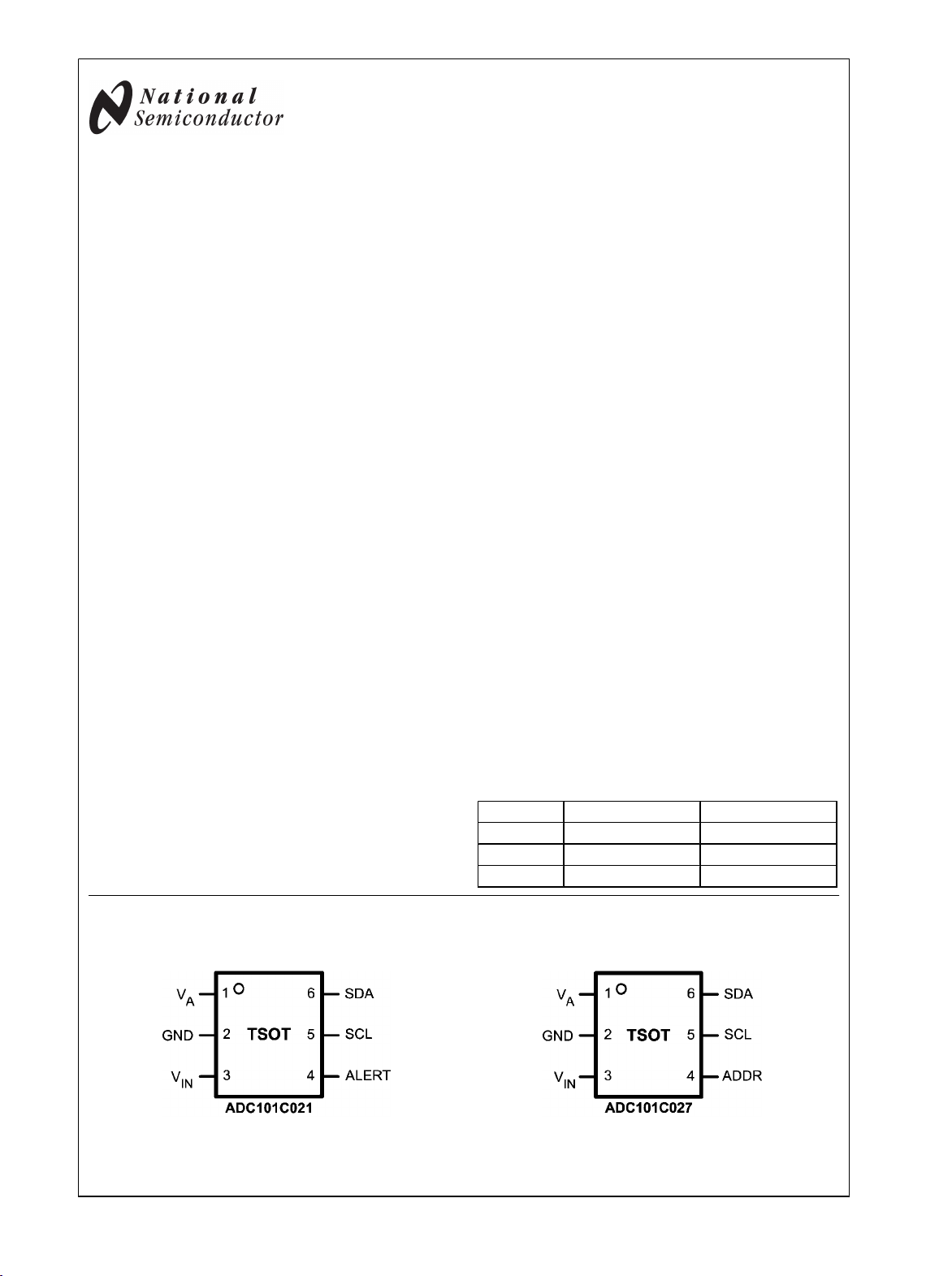
The ADC101C021 comes in a small TSOT-6 package with an
alert output. The ADC101C027 comes in a small TSOT-6
package with an address selection input. The ADC101C027
provides three pin-selectable addresses. Pin-compatible alternatives are available with additional address options.
Normal power consumption using a +3V or +5V supply is
0.26mW or 0.78mW, respectively. The automatic powerdown feature reduces the power consumption to less than
1µW while not converting. Operation over the industrial temperature range of −40°C to +105°C is guaranteed. Their low
power consumption and small packages make this family of
ADCs an excellent choice for use in battery operated equipment.
The ADC101C021 and ADC101C027 are part of a family of
pin-compatible ADCs that also provide 12 and 8 bit resolution.
For 12-bit ADCs see the ADC121C021 and ADC121C027.
For 8-bit ADCs see the ADC081C021 and ADC081C027.
Features
I2C-Compatible 2-wire Interface which supports standard
■
(100kHz), fast (400kHz), and high speed (3.4MHz) modes
Extended power supply range (+2.7V to +5.5V)
■
Up to four pin-selectable chip addresses
■
Out-of-range Alert Function
■
Automatic Power-down mode while not converting
■
Very small 6-pin TSOT packages
■
±8kV HBM ESD protection (SDA, SCL)
■
Key Specifications
Resolution 10 bits; no missing codes
■
Conversion Time 1µs (typ)
■
INL & DNL ±0.5 LSB (max)
■
Throughput Rate 188.9kSPS (max)
■
Power Consumption (at 22kSPS)
■
3V Supply 0.26 mW (typ)
—
5V Supply 0.78 mW (typ)
—
Applications
System Monitoring
■
Peak Detection
■
Portable Instruments
■
Medical Instruments
■
Test Equipment
■
Pin-Compatible Alternatives
All devices are fully pin and function compatible.
Resolution ALERT Output ADDR Input
12-bit ADC121C021 ADC121C027
10-bit ADC101C021 ADC101C027
8-bit ADC081C021 ADC081C027
2
C-Compatible, 10-Bit Analog-to-Digital Converter (ADC) with Alert
Connection Diagrams
30052001 30052002
I2C® is a registered trademark of Phillips Corporation.
© 2008 National Semiconductor Corporation 300520 www.national.com
Ordering Information
Order Code Option Package Top Mark
ADC101C021CIMK Alert pin TSOT-6 X33C
ADC101C021CIMKX Alert pin TSOT-6 Tape-and-Reel X33C
ADC101C027CIMK Address pin TSOT-6 X32C
ADC101C027CIMKX Address pin TSOT-6 Tape-and-Reel X32C
ADC101C021EB
ADC101C021/ADC101C027
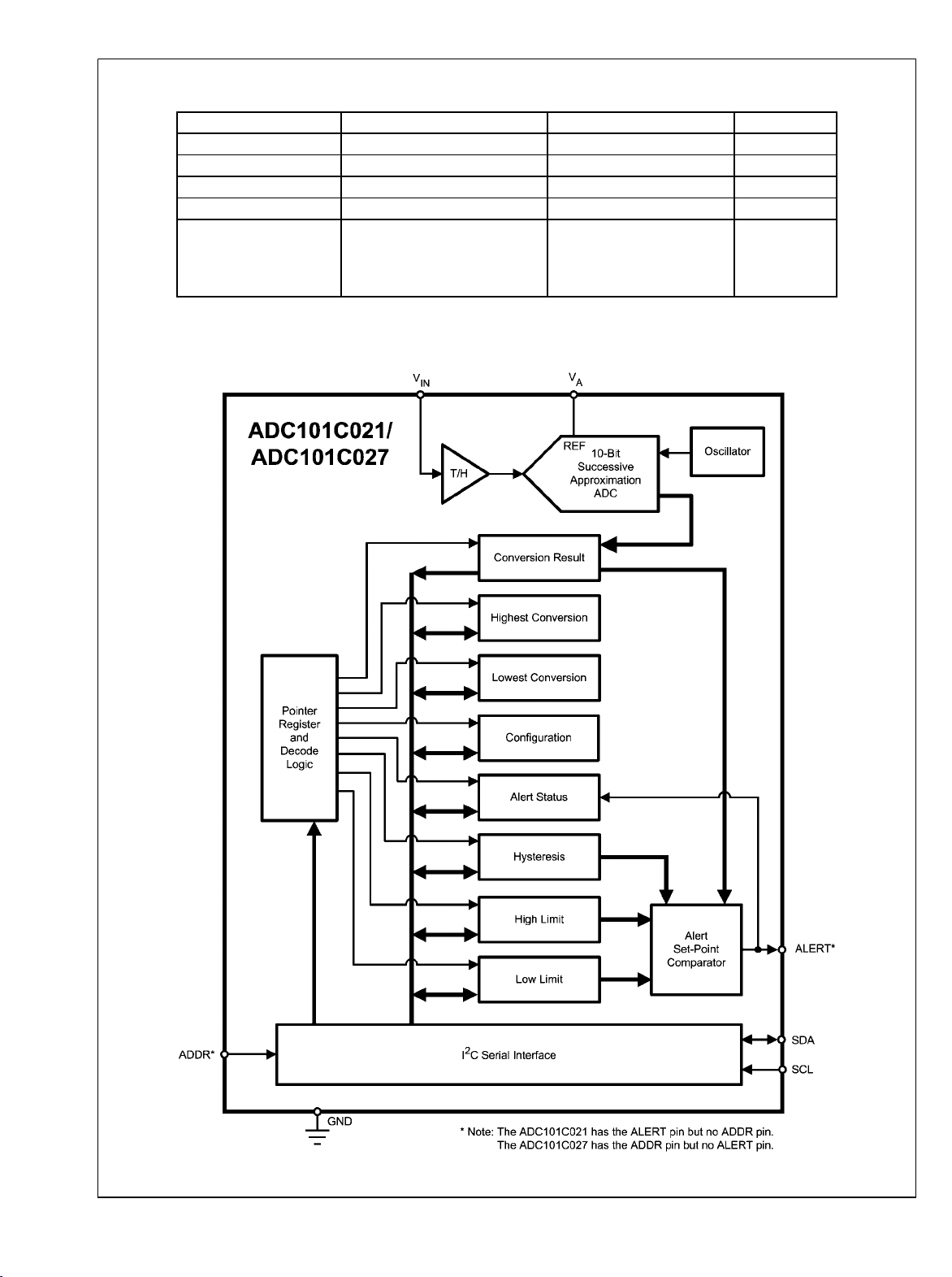
Block Diagram
Shipped with the ADC101C021.
Also compatible with the
ADC101C027 option.
Please order samples.
Evaluation Board
www.national.com 2
30052003
Pin Descriptions
Symbol Type Equivalent Circuit Description
V
A
GND Ground Ground for all on-chip circuitry.
V
IN
ALERT Digital Output
SCL Digital Input
SDA
Supply
Analog Input See Figure 4
Digital
Input/Output
Power and unbufferred reference voltage. VA must be free
of noise and decoupled to GND.
Analog input. This signal can range from GND to VA.
Alert output. Can be configured as active high or active
low. This is an open drain data line that must be pulled to
the supply (VA) with an external pull-up resistor.
Serial Clock Input. SCL is used together with SDA to
control the transfer of data in and out of the device. This is
an open drain data line that must be pulled to the supply
(VA) with an external pull-up resistor. This pin's extended
ESD tolerance( 8kV HBM) allows extension of the I2C bus
across multiple boards without extra ESD protection.
Serial Data bi-directional connection. Data is clocked into
or out of the internal 16-bit register with SCL. This is an
open drain data line that must be pulled to the supply
(VA) with an external pull-up resistor. This pin's extended
ESD tolerance( 8kV HBM) allows extension of the I2C bus
across multiple boards without extra ESD protection.
ADC101C021/ADC101C027
ADDR
Digital Input,
three levels
Package Pinouts
ADC101C021
TSOT-6
ADC101C027
TSOT-6
Tri-level Address Selection Input. Sets Bits A0 & A1 of the
7-bit slave address. (see Table 1)
V
A
1 2 3 4 5 6 N/A
1 2 3 N/A 5 6 4
GND
V
IN
ALERT SCL SDA ADDR
3 www.national.com
Absolute Maximum Ratings
(Notes 1, 2)
If Military/Aerospace specified devices are required,
please contact the National Semiconductor Sales Office/
Distributors for availability and specifications.
Supply Voltage, V
A
-0.3V to +6.5V
Operating Ratings (Notes 1, 2)
Operating Temperature Range
Supply Voltage, V
Analog Input Voltage, V
A
IN
Digital Input Voltage (Note 7) 0V to 5.5V
Sample Rate up to 188.9 kSPS
−40°C ≤ TA ≤ +105°C
+2.7V to 5.5V
Voltage on any Analog Input Pin to
GND
Voltage on any Digital Input Pin to
GND −0.3V to 6.5V
ADC101C021/ADC101C027
Input Current at Any Pin (Note 3) ±15 mA
Package Input Current (Note 3) ±20 mA
Power Dissipation at TA = 25°C
ESD Susceptibility (Note 5)
−0.3V to (VA +0.3V)
See (Note 4)
Package Thermal Resistances
Package
6-Lead TSOT 250°C/W
Soldering process must comply with National
Semiconductor's Reflow Temperature Profile specifications.
Refer to www.national.com/packaging. (Note 6)
θ
JA
VA, GND, VIN, ALERT,
ADDR pins:
Human Body Model
Machine Model
Charged Device Model (CDM)
SDA, SCL pins:
Human Body Model
Machine Model
2500V
250V
1250V
8000V
400V
Junction Temperature +150°C
Storage Temperature −65°C to +150°C
Electrical Characteristics
The following specifications apply for VA = +2.7V to +5.5V, GND = 0V, f
fIN = 10kHz for f
= 3.4MHz unless otherwise noted. Boldface limits apply for TA = T
SCL
unless otherwise noted.
Symbol Parameter Conditions
STATIC CONVERTER CHARACTERISTICS
Resolution with No Missing Codes 10 Bits
VA = +2.7V to +3.6V
VA = +2.7V to +5.5V. f
(Note 13)
INL
Integral Non-Linearity (End Point
Method)
VA = +2.7V to +3.6V
DNL Differential Non-Linearity
VA = +2.7V to +5.5V. f
(Note 13)
VA = +2.7V to +3.6V
f
up to 3.4 MHz
V
OFF
Offset Error
SCL
VA = +2.7V to +5.5V. f
(Note 13)
GE Gain Error -0.13 ±1 LSB (max)
DYNAMIC CONVERTER CHARACTERISTICS
ENOB Effective Number of Bits
SNR Signal-to-Noise Ratio
THD Total Harmonic Distortion
SINAD Signal-to-Noise Plus Distortion Ratio
VA = +2.7V to +3.6V
VA = +3.6V to +5.5V
VA = +2.7V to +3.6V
VA = +3.6V to +5.5V
VA = +2.7V to +3.6V
VA = +3.6V to +5.5V
VA = +2.7V to +3.6V
VA = +3.6V to +5.5V
up to 3.4MHz, fIN = 1kHz for f
SCL
MIN
to T
Typical
(Note 9)
±0.1 ±0.5 LSB (max)
up to 400 kHz
SCL
+0.21 +0.7 LSB (max)
−0.16 −0.7 LSB (min)
±0.1 ±0.5 LSB (max)
up to 400 kHz
SCL
+0.25 +0.7 LSB (max)
−0.16 −0.7 LSB (min)
+0.25 ±0.8 LSB (max)
up to 400kHz
SCL
+0.27 ±0.8 LSB (max)
9.97 9.87 Bits (min)
9.94 Bits
61.8 61.2 dB (min)
61.6 dB
−88.9 −74 dB (max)
−85.7 dB
61.8 61.2 dB (min)
61.6 dB
up to 400kHz,
SCL
: all other limits TA = 25°C
MAX
Limits
(Note 9)
0V to V
A
Units (Limits)
www.national.com 4
ADC101C021/ADC101C027
Symbol Parameter Conditions
SFDR Spurious-Free Dynamic Range
Intermodulation Distortion, Second
IMD
Order Terms (IMD2)
Intermodulation Distortion, Third
Order Terms (IMD3)
FPBW Full Power Bandwidth (−3dB)
VA = +2.7V to +3.6V
VA = +3.6V to +5.5V
fa = 1.035 kHz, fb = 1.135 kHz
fa = 1.035 kHz, fb = 1.135 kHz
VA = +3.0V
VA = +5.0V
Typical
(Note 9)
84 76 dB (min)
84.3 dB
−83.9 dB
−82.4 dB
8 MHz
11 MHz
Limits
(Note 9)
ANALOG INPUT CHARACTERISTICS
I
C
V
DCL
Input Range
IN
DC Leakage Current (Note 10) ±1 µA (max)
Input Capacitance
INA
Track Mode 30 pF
Hold Mode 3 pF
0 to V
A
SERIAL INTERFACE INPUT CHARACTERISTICS (SCL, SDA)
V
V
IH
V
IL
I
IN
C
IN
HYST
Input High Voltage
Input Low Voltage
Input Current (Note 10) ±1 µA (max)
Input Pin Capacitance 3 pF
Input Hysteresis
0.7 x V
0.3 x V
0.1 x V
ADDRESS SELECTION INPUT CHARACTERISTICS (ADDR)
V
V
Input High Voltage
IH
Input Low Voltage 0.5 V (max)
IL
I
Input Current (Note 10) ±1 µA (max)
IN
VA - 0.5V
LOGIC OUTPUT CHARACTERISTICS, OPEN-DRAIN (SDA, ALERT)
I
= 3 mA
V
I
Output Low Voltage
OL
High-Impedence Output
OZ
Leakage Current (Note 10)
SINK
I
= 6 mA
SINK
±1 µA (max)
0.4 V (max)
0.6 V (max)
Output Coding Straight (Natural) Binary
Units (Limits)
A
A
A
V
V (min)
V (max)
V (min)
V (min)
5 www.national.com
Symbol Parameter Conditions
Typical
(Note 9)
POWER REQUIREMENTS
V
Supply Voltage Minimum 2.7 V (min)
A
Supply Voltage Maximum 5.5 V (max)
Continuous Operation Mode -- 2-wire interface active.
VA = 2.7V to 3.6V
VA = 4.5V to 5.5V
VA = 2.7V to 3.6V
VA = 4.5V to 5.5V
VA = 3.0V
VA = 5.0V
VA = 3.0V
VA = 5.0V
I
Supply Current
N
ADC101C021/ADC101C027
P
Power Consumption
N
f
f
f
f
SCL
SCL
SCL
SCL
=400kHz
=3.4MHz
=400kHz
=3.4MHz
Automatic Conversion Mode -- 2-wire interface stopped and quiet (SCL = SDA = VA). f
I
Supply Current
A
P
Power Consumption
A
VA = 2.7V to 3.6V
VA = 4.5V to 5.5V
VA = 3.0V
VA = 5.0V
SAMPLE
0.08 0.14 mA (max)
0.16 0.30 mA (max)
0.37 0.55 mA (max)
0.74 0.99 mA (max)
0.26 mW
0.78 mW
1.22 mW
3.67 mW
= T
CONVERT
0.41 0.59 mA (max)
0.78 1.2 mA (max)
1.35 mW
3.91 mW
Power Down Mode (PD1) -- 2-wire interface stopped and quiet. (SCL = SDA = VA).(Note 10)
I
PD1
P
Supply Current 0.1 0.2 µA (max)
Power Consumption 0.5 0.9 µW (max)
PD1
Power Down Mode (PD2) -- 2-wire interface active. Master communicating with a different device on the bus.
f
=400kHz
SCL
I
PD2
P
Supply Current
Power Consumption
PD2
f
f
f
SCL
SCL
SCL
=3.4MHz
=400kHz
=3.4MHz
VA = 2.7V to 3.6V
VA = 4.5V to 5.5V
VA = 2.7V to 3.6V
VA = 4.5V to 5.5V
VA = 3.0V
VA = 5.0V
VA = 3.0V
VA = 5.0V
13 45 µA (max)
27 80 µA (max)
89 150 µA (max)
168 250 µA (max)
0.04 mW
0.14 mW
0.29 mW
0.84 mW
Limits
(Note 9)
* 32
Units (Limits)
www.national.com 6
A.C. and Timing Characteristics
The following specifications apply for VA = +2.7V to +5.5V. Boldface limits apply for T
TA = 25°C, unless otherwise specified.
Symbol Parameter
Conditions (Note 12)
CONVERSION RATE
Conversion Time 1 µs
f
= 100kHz
SCL
f
= 400kHz
f
CONV
Conversion Rate
SCL
f
= 1.7MHz
SCL
f
= 3.4MHz
SCL
DIGITAL TIMING SPECS (SCL, SDA)
Standard Mode
f
SCL
Serial Clock Frequency
Fast Mode
High Speed Mode, Cb = 100pF
High Speed Mode, Cb = 400pF
Standard Mode
t
LOW
SCL Low Time
Fast Mode
High Speed Mode, Cb = 100pF
High Speed Mode, Cb = 400pF
Standard Mode
t
HIGH
SCL High Time
Fast Mode
High Speed Mode, Cb = 100pF
High Speed Mode, Cb = 400pF
Standard Mode
t
SU;DAT
Data Setup Time
Fast Mode
High Speed Mode
Standard Mode (Note 14)
Fast Mode (Note 14)
t
HD;DAT
Data Hold Time
High Speed Mode, Cb = 100pF
High Speed Mode, Cb = 400pF
Standard Mode
Fast Mode
High Speed Mode
Standard Mode
Fast Mode
High Speed Mode
Standard Mode
Fast Mode
t
SU;STA
t
HD;STA
t
BUF
Setup time for a start or a repeated
start condition
Hold time for a start or a repeated start
condition
Bus free time between a stop and start
condition
Standard Mode
t
SU;STO
Setup time for a stop condition
Fast Mode
High Speed Mode
≤ TA ≤ T
MIN
Typical
(Note 9)
and all other limits are at
MAX
Limits
(Notes 9,
12)
5.56 kSPS
22.2 kSPS
94.4 kSPS
188.9 kSPS
100
400
3.4
1.7
4.7
1.3
160
320
4.0
0.6
60
120
250
100
10
0
3.45
0
0.9
0
70
0
150
4.7
0.6
160
4.0
0.6
160
4.7
1.3
4.0
0.6
160
Units
(Limits)
kHz (max)
kHz (max)
MHz (max)
MHz (max)
us (min)
us (min)
ns (min)
ns (min)
us (min)
us (min)
ns (min)
ns (min)
ns (min)
ns (min)
ns (min)
us (min)
us (max)
us (min)
us (max)
ns (min)
ns (max)
ns (min)
ns (max)
us (min)
us (min)
ns (min)
us (min)
us (min)
ns (min)
us (min)
us (min)
us (min)
us (min)
ns (min)
ADC101C021/ADC101C027
7 www.national.com
Symbol Parameter
t
rDA
Rise time of SDA signal
ADC101C021/ADC101C027
t
fDA
t
rCL
t
rCL1
t
fCL
C
t
SP
b
Fall time of SDA signal
Rise time of SCL signal
Rise time of SCL signal after a
repeated start condition and after an
acknowledge bit.
Fall time of a SCL signal
Capacitive load for each bus line (SCL
and SDA)
Pulse Width of spike suppressed
(Note 11)
Limits
(Notes 9,
12)
Units
(Limits)
Conditions (Note 12)
Typical
(Note 9)
Standard Mode 1000 ns (max)
Fast Mode
High Speed Mode, Cb = 100pF
High Speed Mode, Cb = 400pF
20+0.1C
300
10
80
20
160
b
ns (min)
ns (max)
ns (min)
ns (max)
ns (min)
ns (max)
Standard Mode 250 ns (max)
Fast Mode
High Speed Mode, Cb = 100pF
High Speed Mode, Cb = 400pF
20+0.1C
250
10
80
20
160
b
ns (min)
ns (max)
ns (min)
ns (max)
ns (min)
ns (max)
Standard Mode 1000 ns (max)
Fast Mode
High Speed Mode, Cb = 100pF
High Speed Mode, Cb = 400pF
20+0.1C
300
10
40
20
80
b
ns (min)
ns (max)
ns (min)
ns (max)
ns (min)
ns (max)
Standard Mode 1000 ns (max)
Fast Mode
High Speed Mode, Cb = 100pF
High Speed Mode, Cb = 400pF
20+0.1C
300
10
80
20
160
b
ns (min)
ns (max)
ns (min)
ns (max)
ns (min)
ns (max)
Standard Mode 300 ns (max)
Fast Mode
High Speed Mode, Cb = 100pF
High Speed Mode, Cb = 400pF
20+0.1C
300
10
40
20
80
b
ns (min)
ns (max)
ns (min)
ns (max)
ns (min)
ns (max)
400 pF (max)
Fast Mode
High Speed Mode
50
10
ns (max)
ns (max)
Note 1: Absolute Maximum Ratings indicate limits beyond which damage to the device may occur. Operating Ratings indicate conditions for which the device is
functional, but do not guarantee specific performance limits. For guaranteed specifications and test conditions, see the Electrical Characteristics. The guaranteed
specifications apply only for the test conditions listed. Some performance characteristics may degrade when the device is not operated under the listed test
conditions. Operation of the device beyond the maximum Operating Ratings is not recommended.
Note 2: All voltages are measured with respect to GND = 0V, unless otherwise specified.
Note 3: When the input voltage at any pin exceeds 5.5V or is less than GND, the current at that pin should be limited per the Absolute Maximum Ratings. The
mximum package input current rating limits the number of pins that can safely exceed the power supplies.
Note 4: The absolute maximum junction temperature (TJmax) for this device is 150°C. The maximum allowable power dissipation is dictated by TJmax, the
junction-to-ambient thermal resistance (θJA), and the ambient temperature (TA), and can be calculated using the formula PDMAX = (TJmax − TA) / θJA. The values
for maximum power dissipation will be reached only when the device is operated in a severe fault condition (e.g., when input or output pins are driven beyond
the operating ratings, or the power supply polarity is reversed).
Note 5: Human body model is a 100 pF capacitor discharged through a 1.5 kΩ resistor. Machine model is a 220 pF capacitor discharged through 0 Ω. Charged
device model simulates a pin slowly acquiring charge (such as from a device sliding down the feeder in an automated assembler) then rapidly being discharged.
Note 6: Reflow temperature profiles are different for lead-free packages.
www.national.com 8
Note 7: The inputs are protected as shown below. Input voltage magnitudes up to 5.5V, regardless of VA, will not cause errors in the conversion result. For
example, if VA is 3V, the digital input pins can be driven with a 5V logic device.
30052004
Note 8: To guarantee accuracy, it is required that VA be well bypassed and free of noise.
Note 9: Typical figures are at TJ = 25°C, and represent most likely parametric norms. Test limits are guaranteed to National's AOQL (Average Outgoing Quality
Level).
Note 10: This parameter is guaranteed by design and/or characterization and is not tested in production.
Note 11: Spike suppression filtering on SCL and SDA will supress spikes that are less than 50ns for standard and fast modes, and less than 10ns for hs-mode.
Note 12: Cb refers to the capacitance of one bus line. Cb is expressed in pF units.
Note 13: The ADC will meet Minimum/Maximum specifications for f
Note 14: The ADC101C021 will provide a minimum data hold time of 300ns to comply with the I2C Specification.
up to 3.4MHz when operating in the Quiet Interface Mode (Section 1.11).
SCL
Timing Diagrams
ADC101C021/ADC101C027
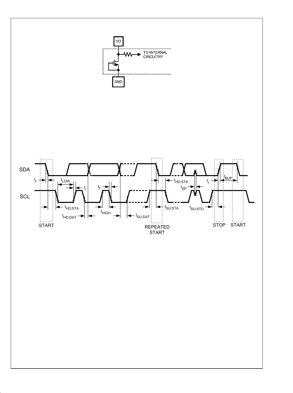
FIGURE 1. Serial Timing Diagram
9 www.national.com
30052060
Specification Definitions
ACQUISITION TIME is the time required for the ADC to ac-
quire the input voltage. During this time, the hold capacitor is
charged by the input voltage.
APERTURE DELAY is the time between the start of a conversion and the time when the input signal is internally acquired or held for conversion.
CONVERSION TIME is the time required, after the input voltage is acquired, for the ADC to convert the input voltage to a
digital word.
DIFFERENTIAL NON-LINEARITY (DNL) is the measure of
ADC101C021/ADC101C027
the maximum deviation from the ideal step size of 1 LSB.
EFFECTIVE NUMBER OF BITS (ENOB, or EFFECTIVE
BITS) is another method of specifying Signal-to-Noise and
Distortion or SINAD. ENOB is defined as (SINAD - 1.76) / 6.02
and says that the converter is equivalent to a perfect ADC of
this (ENOB) number of bits.
FULL POWER BANDWIDTH is a measure of the frequency
at which the reconstructed output fundamental drops 3 dB
below its low frequency value for a full scale input.
GAIN ERROR is the deviation of the last code transition
(111...110) to (111...111) from the ideal (V
adjusting for offset error.
INTEGRAL NON-LINEARITY (INL) is a measure of the deviation of each individual code from a line drawn from negative
full scale (½ LSB below the first code transition) through positive full scale (½ LSB above the last code transition). The
deviation of any given code from this straight line is measured
from the center of that code value.
INTERMODULATION DISTORTION (IMD) is the creation of
additional spectral components as a result of two sinusoidal
frequencies being applied to an individual ADC input at the
same time. It is defined as the ratio of the power in either the
second or the third order intermodulation products to the sum
of the power in both of the original frequencies. Second order
products are fa ± fb, where fa and fb are the two sine wave
input frequencies. Third order products are (2fa ± fb ) and
(fa ± 2fb). IMD is usually expressed in dB.
MISSING CODES are those output codes that will never appear at the ADC output. The ADC101C021 is guaranteed not
to have any missing codes.
OFFSET ERROR is the deviation of the first code transition
(000...000) to (000...001) from the ideal (i.e. GND + 0.5 LSB).
- 1.5 LSB), after
REF
SIGNAL TO NOISE RATIO (SNR) is the ratio, expressed in
dB, of the rms value of the input signal to the rms value of the
sum of all other spectral components below one-half the sampling frequency, not including harmonics or d.c.
SIGNAL TO NOISE PLUS DISTORTION (S/N+D or
SINAD) Is the ratio, expressed in dB, of the rms value of the
input signal to the rms value of all of the other spectral components below half the clock frequency, including harmonics
but excluding d.c.
SPURIOUS FREE DYNAMIC RANGE (SFDR) is the difference, expressed in dB, between the desired signal amplitude
to the amplitude of the peak spurious spectral component,
where a spurious spectral component is any signal present in
the output spectrum that is not present at the input and may
or may not be a harmonic.
TOTAL HARMONIC DISTORTION (THD) is the ratio, expressed in dBc, of the rms total of the first n harmonic components at the output to the rms level of the input signal
frequency as seen at the output. THD is calculated as
where Af1 is the RMS power of the input frequency at the output and Af2 through Afn are the RMS power in the first n
harmonic frequencies.
THROUGHPUT TIME is the minimum time required between
the start of two successive conversions. It is the acquisition
time plus the conversion time.
LEAST SIGNIFICANT BIT (LSB) is the bit that has the smallest value or weight of all bits in a word. This value is
LSB = VA / 2
where VA is the supply voltage for this product, and "n" is the
resolution in bits, which is 10 for the ADC101C021.
MOST SIGNIFICANT BIT (MSB) is the bit that has the largest
value or weight of all bits in a word. Its value is 1/2 of VA.
n
www.national.com 10
ADC101C021/ADC101C027
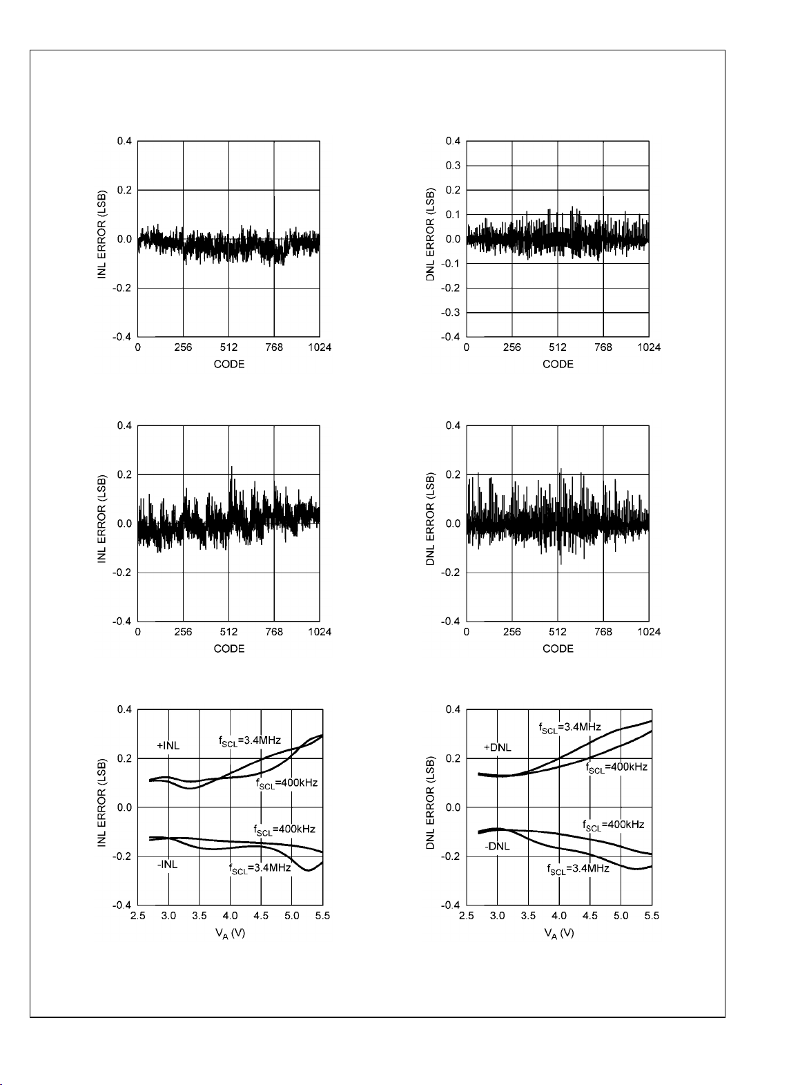
Typical Performance Characteristics f
+25°C, unless otherwise stated.
INL vs. Code - VA=3V
30052022
INL vs. Code - VA=5V
= 400kHz, f
SCL
= 22kSPS, fIN = 1kHz, VA = 5.0V, TA =
SAMPLE
DNL vs. Code - VA=3V
DNL vs. Code - VA=5V
30052023
INL vs. Supply
30052024
30052026
30052025
DNL vs. Supply
30052027
11 www.national.com
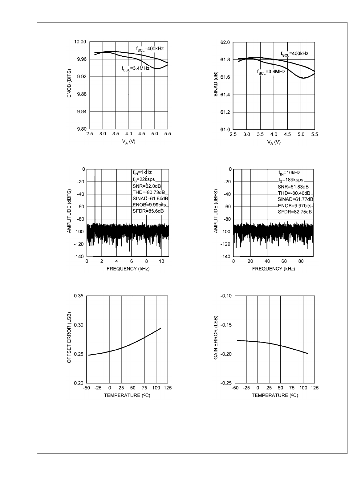
ENOB vs. Supply
ADC101C021/ADC101C027
SINAD vs. Supply
FFT Plot - VA=3V
Offset Error vs. Temperature
30052028
30052030
30052029
FFT Plot - VA=3V
30052031
Gain Error vs. Temperature
30052032
www.national.com 12
30052033
ADC101C021/ADC101C027
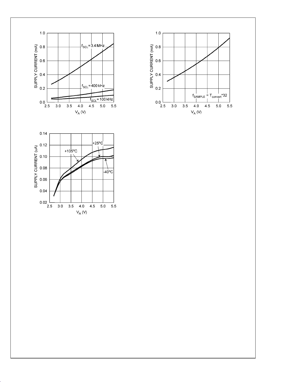
Continuous Operation Supply Current vs. V
30052034
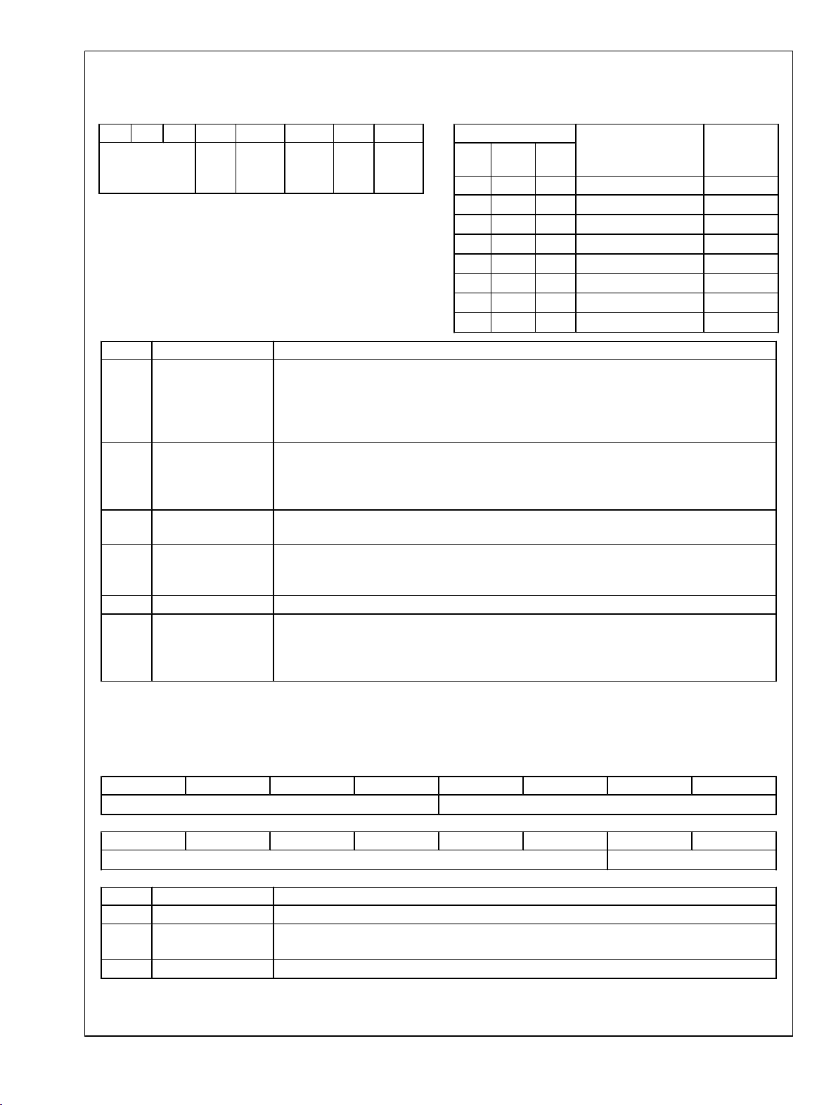
Power Down (PD1) Supply Current vs. V
A
A
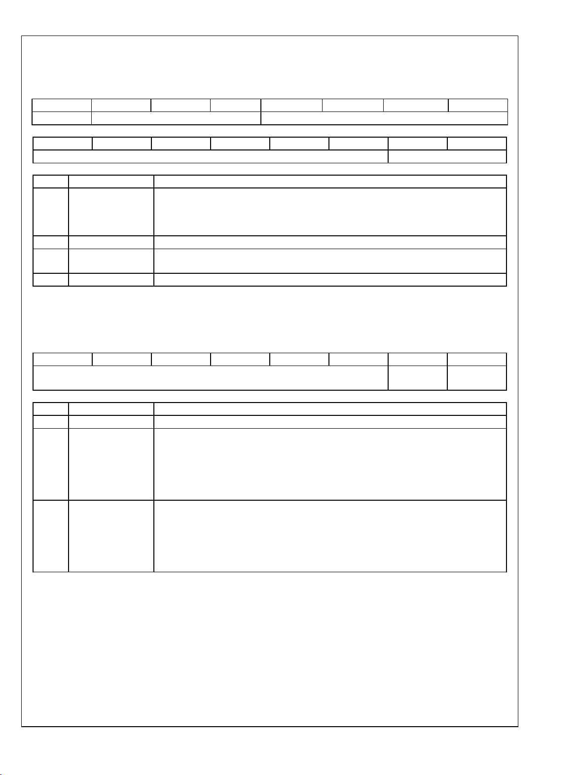
Automatic Conversion Supply Current vs. V
30052035
A
30052036
13 www.national.com

1.0 Functional Description
The ADC101C021 is a successive-approximation analog-todigital converter designed around a charge-redistribution digital-to-analog converter. Unless otherwise stated, references
to the ADC101C021 in this section will apply to both the
ADC101C021 and the ADC101C027.
1.1 CONVERTER OPERATION
Simplified schematics of the ADC101C021 in both track and
hold operation are shown in Figure 2 and Figure 3 respectively. In Figure 2, the ADC101C021 is in track mode; switch
SW1 connects the sampling capacitor to the analog input
ADC101C021/ADC101C027
channel, and SW2 equalizes the comparator inputs. The ADC
is in this state for approximately 0.4µs at the beginning of every conversion cycle. Conversions occur when the conversion result register is read by the I2C controller and when the
ADC is in automatic conversion mode. (see Section 1.9)
Figure 3 shows the ADC101C021 in hold mode: switch SW1
connects the sampling capacitor to ground and switch SW2
unbalances the comparator. The control logic then instructs
the charge-redistribution DAC to add or subtract fixed
amounts of charge to or from the sampling capacitor until the
comparator is balanced. When the comparator is balanced,
the digital word supplied to the DAC is also the digital representation of the analog input voltage. This digital word is
stored in the conversion result register and read via the 2-wire
interface.
1.2 ANALOG INPUT
An equivalent circuit for the input of the ADC101C021 is
shown in Figure 4. Diodes D1 and D2 provide ESD protection
for the analog input. The operating range for the analog input
is 0 V to VA. Going beyond this range will cause the ESD
diodes to conduct and result in erratic operation.
The capacitor C1 in Figure 4 has a typical value of 3 pF and
is mainly the package pin capacitance. Resistor R1 is the on
resistance (RON) of the multiplexer and track / hold switch and
is typically 500Ω. Capacitor C2 is the ADC101C021 sampling
capacitor, and is typically 30 pF. The ADC101C021 will deliver best performance when driven by a low-impedance
source (less than 100Ω). This is especially important when
using the ADC101C021 to sample dynamic signals. The dynamic performance of the ADC will be affected significantly
by large source impedances. An input buffer amplifier may be
necessary to limit source impedance. A high-accuracy opamp is recommended to maximize circuit performance. Also
important when sampling dynamic signals is an anti-aliasing
band-pass or low-pass filter which reduces harmonics and
noise at the input.
FIGURE 2. ADC101C021 in Track Mode
FIGURE 3. ADC101C021 in Hold Mode
30052067
FIGURE 4. Equivalent Input Circuit
30052065
30052066
www.national.com 14

ADC101C021/ADC101C027
1.3 ADC TRANSFER FUNCTION
The output format of the ADC101C021 is straight binary.
Code transitions occur midway between successive integer
LSB values. The LSB width for the ADC101C021 is VA / 1024.
The ideal transfer characteristic is shown in Figure 5. The
transition from an output code of 0000 0000 0000 to a code
of 0000 0000 0001 is at 1/2 LSB, or a voltage of VA / 2048.
Other code transitions occur at intervals of 1 LSB.
30052068
FIGURE 5. Ideal Transfer Characteristic
1.4 REFERENCE VOLTAGE
The ADC101C021 uses the supply (VA) as the reference.
With that said, VA must be treated as a reference. The analogto-digital conversion will only be as precise as the reference
(VA). Therefore, the reference (VA) should be free of noise. It
is also recommended that the reference be driven by a voltage source with low output impedance.
The Applications section provides recommended ways to
drive the reference (VA) appropriately. Refer to Section 2.1 for
details.
1.5 POWER-ON RESET
The power-on reset (POR) state is the point at which the supply voltage rises above the power-on reset threshold, generating an internal reset. Each of the registers contains a
defined value upon POR and this data remains there until any
of the following occurs:
•
The first conversion is completed, causing the Conversion
Result Register and various status registers to be updated
internally.
•
The master writes a different data word to any of the
writeable registers.
•
The ADC is powered down.
When resetting the device, it is crutial that the VA supply be
lowered to a maximum of 200mV before the supply is raised
again to power-up the device. Dropping the supply to within
200mV of GND during a reset will ensure the ADC performs
as specified.
15 www.national.com

1.6 INTERNAL REGISTERS
The ADC101C021 is equipped with 8 internal data registers
and one address pointer register. The registers provide additional ADC functions such as storing minimum and maximum
conversion results, setting alert threshold levels, and storing
data to configure the operation of the device. Figure 6 shows
all of the registers and their corresponding address pointer
values. All of the registers are read/write capable except the
conversion result register which is read-only.
ADC101C021/ADC101C027
1.6.1 Address Pointer Register
The address pointer register controls which of the data registers is accessed by the I2C interface. The first data byte of
every write operation is stored in the address pointer register.
This value selects the register that the following data bytes
will be written to or read from. Only the three LSBs of this
register are relevant. The other bits must always be written as
zeros. After a power-on reset, the pointer register defaults to
all zeros (conversion result register).
Default Value: 00h
P7 P6 P5 P4 P3 P2 P1 P0
0 0 0 0 0 Register Select
P2 P1 P0 REGISTER
0 0 0 Conversion Result (read only)
0 0 1 Alert Status (read/write)
0 1 0 Configuration (read/write)
0 1 1 Low Limit (read/write)
1 0 0 High Limit (read/write)
1 0 1 Hysteresis (read/write)
1 1 0 Lowest Conversion (read/write)
1 1 1 Highest Conversion (read/write)
30052069
FIGURE 6. Register Structure
www.national.com 16
1.6.2 Conversion Result Register
Pointer Address 00h (Read Only)
Default Value: 0000h
D15 D14 D13 D12 D11 D10 D9 D8
Alert Flag Reserved Conversion Result[9:6]
D7 D6 D5 D4 D3 D2 D1 D0
Conversion Result[5:0] Reserved
Bits Name Description
15 Alert Flag When the Alert Bit Enable is set in the Configuration Register, this bit will be high if either alert
flag is set in the Alert Status Register. Otherwise, this bit is a zero. This bit indicates that an alert
condition has occured. The I2C controller will typically read the Alert Status register and other
data registers to determine the source of the alert.
14:12 Reserved Always reads zeros.
11:2 Conversion Result The Analog-to-Digital conversion result. The Conversion result data is a 10-bit data word in
straight binary format. The MSB is D11.
1:0 Reserved Always reads zeros.
1.6.3 Alert Status Register
Pointer Address 01h (Read/Write)
Default Value: 00h
ADC101C021/ADC101C027
D7 D6 D5 D4 D3 D2 D1 D0
Reserved Over Range
Alert
Bits Name Description
7:2 Reserved Always reads zeros. Zeros must be written to these bits.
1 Over Range
Alert Flag
Bit is set to 1 when the measured voltage exceeds the V
V
limit register. Flag is reset to 0 when one of the following two conditions is met: (1) The
HIGH
limit stored in the programmable
HIGH
controller writes a one to this bit. (2) The measured voltage decreases below the programmed
V
limit minus the programmed V
HIGH
value (See Figure 9) . The alert will only self-clear if the
HYST
Alert Hold bit is cleared in the Configuration register. If the Alert Hold bit is set, the only way to
clear an over range alert is to write a one to this bit.
0 Under Range
Alert Flag
Bit is set to 1 when the measured voltage falls below the V
V
limit register. Flag is reset to 0 when one of the following two conditions is met: (1) The
LOW
limit stored in the programmable
LOW
controller writes a one to this bit. (2) The measured voltage increases above the programmed
V
limit plus the programmed V
LOW
value. The alert will only self-clear if the Alert Hold bit is
HYST
cleared in the Configuration register. If the Alert Hold bit is set, the only way to clear an under
range alert is to write a one to this bit.
Under Range
Alert
17 www.national.com
1.6.4 Configuration Register
Pointer Address 02h (Read/Write)
Default Value: 00h
D7 D6 D5 D4 D3 D2 D1 D0
Cycle Time [2:0] Alert
Hold
Alert
Flag
Enable
Alert
Pin
Enable
ADC101C021/ADC101C027
0 Polarity
Cycle Time[2:0] Conversion
D7 D6 D5
Interval
0 0 0 Mode Disabled 0
0 0 1 T
0 1 0 T
0 1 1 T
1 0 0 T
1 0 1 T
1 1 0 T
1 1 1 T
x 32 27
convert
x 64 13.5
convert
x 128 6.7
convert
x 256 3.4
convert
x 512 1.7
convert
x 1024 0.9
convert
x 2048 0.4
convert
Bits Name Description
7:5 Cycle Time Configures Automatic Conversion mode. When these bits are set to zeros, the automatic
conversion mode is disabled. This is the case at power-up.
When these bits are set to a non-zero value, the ADC will begin operating in automatic conversion
mode. (See Section 1.9). The Cycle Time table shows how different values provide various
conversion intervals.
4 Alert Hold 0: Alerts will self-clear when the measured voltage moves within the limits by more than the
hysteresis register value.
1: Alerts will not self-clear and are only cleared when a one is written to the alert high flag or the
alert low flag in the Alert Status register.
3 Alert Flag Enable 0: Disables alert status bit [D15] in the Conversion Result register.
1: Enables alert status bit [D15] in the Conversion Result register.
2 Alert Pin Enable 0: Disables the ALERT output pin. The ALERT output will TRI-STATE when the pin is disabled.
1: Enables the ALERT output pin.
*This bit does not apply to the ADC101C027.
1 Reserved Always reads zeros. Zeros must be written to these bits.
0 Polarity This bit configures the active level polarity of the ALERT output pin.
0: Sets the ALERT pin to active low.
1: Sets the ALERT pin to active high.
*This bit does not apply to the ADC101C027.
Typical
f
convert
(kSPS)
1.6.5 V
-- Alert Limit Register - Under Range
LOW
Pointer Address 03h (Read/Write)
Default Value: 0000h
D15 D14 D13 D12 D11 D10 D9 D8
Reserved V
D7 D6 D5 D4 D3 D2 D1 D0
V
Limit[5:0] Reserved
LOW
Bits Name Description
15:12 Reserved Always reads zeros. Zeros must be written to these bits.
11:2 V
Limit Sets the lower limit threshold used to determine the alert condition. If the conversion moves lower
LOW
than this limit, a V
alert is generated.
LOW
1:0 Reserved Always reads zeros. Zeros must be written to these bits.
www.national.com 18
LOW
Limit[9:6]

ADC101C021/ADC101C027
1.6.6 V
-- Alert Limit Register - Over Range
HIGH
Pointer Address 04h (Read/Write)
Default Value: 0FFFh
D15 D14 D13 D12 D11 D10 D9 D8
Reserved V
HIGH
Limit[9:6]
D7 D6 D5 D4 D3 D2 D1 D0
V
Limit[5:0] Reserved
HIGH
Bits Name Description
15:12 Reserved Always reads zeros. Zeros must be written to these bits.
11:2 V
Limit Sets the upper limit threshold used to determine the alert condition. If the conversion moves
HIGH
higher than this limit, a V
alert is generated.
HIGH
1:0 Reserved Always reads zeros. Zeros must be written to these bits.
1.6.7 V
-- Alert Hysteresis Register
HYST
Pointer Address 05h (Read/Write)
Default Value: 0000h
D15 D14 D13 D12 D11 D10 D9 D8
Reserved Hysteresis[9:6]
D7 D6 D5 D4 D3 D2 D1 D0
Hysteresis[5:0] Reserved
Bits Name Description
15:12 Reserved Always reads zeros. Zeros must be written to these bits.
11:2 Hysteresis Sets the hysteresis value used to determine the alert condition. After a V
the conversion result must move within the V
HIGH
or V
limit by more than this value to clear
LOW
HIGH
or V
the alert condition.
Note: If the Alert Hold bit is set in the configuration register, alert conditions will not self-clear.
1:0 Reserved Always reads zeros. Zeros must be written to these bits.
alert occurs,
LOW
19 www.national.com
1.6.8 V
-- Lowest Conversion Register
MIN
Pointer Address 06h (Read/Write)
Default Value: 0FFFh
D15 D14 D13 D12 D11 D10 D9 D8
Reserved Lowest Conversion[9:6]
D7 D6 D5 D4 D3 D2 D1 D0
Lowest Conversion[5:0] Reserved
ADC101C021/ADC101C027
Bits Name Description
15:12 Reserved Always reads zeros. Zeros must be written to these bits.
11:2 Lowest Conversion Contains the Lowest Conversion result. Each conversion result is compared against the contents
of this register. If the value is lower, it becomes the lowest conversion and replaces the current
value. If the value is higher, the register contents remain unchanged. The lowest conversion value
can be cleared at any time by writting 0FFFh to this register. The value of this register will update
automatically when the automatic conversion mode is enabled.
1:0 Reserved Always reads zeros. Zeros must be written to these bits.
1.6.9 V
-- Highest Conversion Register
MAX
Pointer Address 07h (Read/Write)
Default Value: 0000h
D15 D14 D13 D12 D11 D10 D9 D8
Reserved Highest Conversion[9:6]
D7 D6 D5 D4 D3 D2 D1 D0
Highest Conversion[5:0] Reserved
Bits Name Description
15:12 Reserved Always reads zeros. Zeros must be written to these bits.
11:2 Highest Conversion Contains the Highest Conversion result. Each conversion result is compared against the contents
of this register. If the value is higher, it becomes the highest conversion and replaces the previous
value. If the value is lower, the register contents remain unchanged. The highest conversion value
can be cleared at any time by writting 0000h to this register. The value of this register will update
automatically when the automatic conversion mode is enabled.
1:0 Reserved Always reads zeros. Zeros must be written to these bits.
www.national.com 20

ADC101C021/ADC101C027
1.7 SERIAL INTERFACE
The I2C-compatible interface operates in all three speed
modes. Standard mode (100kHz) and Fast mode (400kHz)
are functionally the same and will be referred to as StandardFast mode in this document. High-Speed mode (3.4MHz) is
an extension of Standard-Fast mode and will be referred to
as Hs-mode in this document. The following diagrams describe the timing relationships of the clock (SCL) and data
(SDA) signals. Pull-up resistors or current sources are required on the SCL and SDA busses to pull them high when
they are not being driven low. A logic zero is transmitted by
driving the output low. A logic high is transmitted by releasing
the output and allowing it to be pulled-up externally. The appropriate pull-up resistor values will depend upon the total bus
capacitance and operating speed. The ADC101C021 offers
extended ESD tolerance (8kV HBM) for the I2C bus pins (SCL
& SDA) allowing extension of the bus across multiple boards
without extra ESD protection.
1.7.1 Basic I2C Protocol
The I2C interface is bi-directional and allows multiple devices
to operate on the same bus. The bus consists of master devices and slave devices which can communicate back and
forth over the I2C interface. Master devices control the bus
and are typically microcontrollers, FPGAs, DSPs, or other
digital controllers. Slave devices are controlled by a master
and are typically peripheral devices such as the
ADC101C021. To support multiple devices on the same bus,
each slave has a unique hardware address which is referred
to as the "slave address." To communicate with a particular
device on the bus, the controller (master) sends the slave address and listens for a response from the slave. This response
is referred to as an acknowledge bit. If a slave on the bus is
addressed correctly, it Acknowledges(ACKs) the master by
driving the SDA bus low. If the address doesn't match a
device's slave address, it Not-acknowledges(NACKs) the
master by letting SDA be pulled high. ACKs also occur on the
bus when data is being transmitted. When the master is writing data, the slave ACKs after every data byte is successfully
received. When the master is reading data, the master ACKs
after every data byte is received to let the slave know it wants
to receive another data byte. When the master wants to stop
reading, it NACKs after the last data byte and creates a stop
condition on the bus.
All communication on the bus begins with either a Start condition or a Repeated Start condition. The protocol for starting
the bus varies between Standard-Fast mode and Hs-mode.
In Standard-Fast mode, the master generates a
Start condition by driving SDA from high to low while SCL is
high. In Hs-mode, starting the bus is more complicated.
Please refer to section 1.7.3 for the full details of a Hs-mode
Start condition. A Repeated Start is generated to address a
different device or register, or to switch between read and
write modes. The master generates a Repeated Start condition by driving SDA low while SCL is high. Following the
Repeated Start, the master sends out the slave address and
a read/write bit as shown in Figure 7. The bus continues to
operate in the same speed mode as before the Repeated
Start condition.
All communication on the bus ends with a Stop condition. In
either Standard-Fast mode or Hs-Mode, a Stop condition occurs when SDA is pulled from low to high while SCL is high.
After a Stop condition, the bus remains idle until a master
generates a Start condition.
Please refer to the Philips I2C® Specification (Version 2.1 Jan,
2000) for a detailed description of the serial interface.
FIGURE 7. Basic Operation.
1.7.2 Standard-Fast Mode
In Standard-Fast mode, the master generates a start condition by driving SDA from high to low while SCL is high. The
start condition is always followed by a 7-bit slave address and
a Read/Write bit. After these 8 bits have been transmitted by
the master, SDA is released by the master and the
ADC101C021 either ACKs or NACKs the address. If the slave
address matches, the ADC101C021 ACKs the master. If the
address doesn't match, the ADC101C021 NACKs the master.
For a write operation, the master follows the ACK by sending
the 8-bit register address pointer to the ADC. Then the
ADC101C021 ACKs the transfer by driving SDA low. Next,
the master sends the upper 8-bits to the ADC101C021. Then
30052011
the ADC101C021 ACKs the transfer by driving SDA low. For
a single byte transfer, the master should generate a stop condition at this point. For a 2-byte write operation, the lower 8bits are sent by the master. The ADC101C021 then ACKs the
transfer, and the master either sends another pair of data
bytes, generates a Repeated Start condition to read or write
another register, or generates a Stop condition to end communication.
A read operation can take place either of two ways:
If the address pointer is pre-set before the read operation, the
desired register can be read immediately following the slave
address. In this case, the upper 8-bits of the register, set by
the pre-set address pointer, are sent out by the ADC. For a
21 www.national.com

single byte read operation, the Master sends a NACK to the
ADC and generates a Stop condition to end communication
after receiving 8-bits of data. For a 2-byte read operation, the
Master continues the transmission by sending an ACK to the
ADC. Then, the ADC sends out the lower 8-bits of the ADC
register. At this point, the master either sends; an ACK to receive more data or, a NACK followed by a Stop or Repeated
Start. If the master sends an ACK, the ADC sends the next
upper data byte, and the read cycle repeats.
If the address pointer needs to be set, the ADC101C021
needs to write to the device and set the address pointer before
reading from the desired register. This type of read requires
ADC101C021/ADC101C027
a start, the slave address, a write bit, the address pointer, a
Repeated Start, the slave address, and a read bit (refer to
Figure 12). Following this sequence, the ADC sends out the
upper 8-bits of the register. For a single byte read operation,
the Master must send a NACK to the ADC and generate a
Stop condition to end communication. For a 2-Byte write operation, the Master sends an ACK to the ADC. Then, the ADC
sends out the lower 8-bits of the ADC register. At this point,
the master sends either an ACK to receive more data, or a
NACK followed by a Stop or Repeated Start. If the master
sends an ACK, the ADC sends another pair of data bytes, and
the read cycle will repeat. The number of data words that can
be read is unlimited.
1.7.3 High-Speed (Hs) Mode
For Hs-mode, the sequence of events to begin communication differs slightly from Standard-Fast mode. Figure 8 describes this in further detail. Initially, the bus begins running
in Standard-Fast mode. The master generates a
Start condition and sends the 8-bit Hs master code
(00001XXX) to the ADC101C021. Next, the ADC101C021
responds with a NACK. Once the SCL line has been pulled to
a high level, the master switches to Hs-mode by increasing
the bus speed and generating a Repeated Start condition
(driving SDA low while SCL is pulled high). At this point, the
master sends the slave address to the ADC101C021, and
communication continues as shown above in the "Basic Operation" Diagram (see Figure 7).
When the master generates a Repeated Start condition while
in Hs-mode, the bus stays in Hs-mode awaiting the slave address from the master. The bus continues to run in Hs-mode
until a Stop condition is generated by the master. When the
master generates a Stop condition on the bus, the bus must
be started in Standard-Fast mode again before increasing the
bus speed and switching to Hs-mode.
FIGURE 8. Beginning Hs-Mode Communication
1.7.4 I2C Slave (Hardware) Address
The ADC has a seven-bit hardware address which is also referred to as a slave address. For the ADC101C027, the
address is configured by the ADDR address selection input.
ADDR can be grounded, left floating, or tied to VA. If desired,
ADDR can be set to VA/2 rather than left floating. The state of
the ADDR input sets the hardware address that the ADC responds to on the I2C bus (see Table 1). For the
ADC101C021, the hardware address is not pin-configurable
and is set to 1010100. The diagrams in Section 1.10 describe
how the I2C controller should address the ADC via the I2C
interface.
30052012
TABLE 1. Slave Addresses
Slave Address
[A6 - A0]
ADC101C027*
ADDR
ADC101C021*
1010000 Floating -----------------
1010001 GND -----------------
1010010 V
A
-----------------
1010100 ----------------- Single Address
1010101 ----------------- -----------------
1010110 ----------------- -----------------
1011000 ----------------- -----------------
1011001 ----------------- -----------------
1011010 ----------------- -----------------
* Pin-compatible alternatives to the ADC101C021 and the
ADC101C027 are available with additional address options.
www.national.com 22

1.8 ALERT FUNCTION
The ALERT function is an "out-of-range" indicator. At the end
of every conversion, the measured voltage is compared to the
values in the V
age exceeds the value stored in V
stored in V
is indicated in up to three places. First, the alert condition al-
LOW
and V
HIGH
, an alert condition occurs. The Alert condition
registers. If the measured volt-
LOW
or falls below the value
HIGH
ways causes either or both of the alert flags in the Alert Status
register to go high. If the measured voltage exceeds the
V
limit, the Over Range Alert Flag is set. If the measured
HIGH
voltage falls below the V
is set. Second, if the Alert Flag Enable bit is set in the Con-
limit, the Under Range Alert Flag
LOW
figuration register, the alert condition also sets the MSB of the
Conversion Result register. Third, if the Alert Pin Enable bit is
set in the Configuration register, the ALERT output becomes
active (see Figure 9). The ALERT output can be configured
as an active high or active low output via the Polarity bit in the
Configuration register. If the Polarity bit is cleared, the ALERT
output is configured as active low. If the Polarity bit is set, the
ALERT output is configured as active high.
The Over Range Alert condition is cleared when one of the
following two conditions is met:
1.
The controller writes a one to the Over Range Alert Flag
bit.
2.
The measured voltage reduces below the programmed
V
limit minus the programmed V
HIGH
Alert Hold bit is cleared in the Configuration register. (see
value and the
HYST
Figure 9). If the Alert Hold bit is set, the alert condition
persists and only clears when a one is written to the Over
Range Alert Flag bit.
The Under Range Alert condition is cleared when one of the
following two conditions is met:
1.
The controller writes a one to the Under Range Alert Flag
bit.
2.
The measured voltage increases above the programmed
V
limit plus the programmed V
LOW
Alert Hold bit is cleared in the Configuration register. If
value and the
HYST
the Alert Hold bit is set, the alert condition persists and
only clears when a one is written to the Under Range
Alert Flag bit.
If the alert condition has been cleared by writing a one to the
alert flag while the measured voltage still violates the V
or V
completion of the next conversion (see Figure 10).
limits, an alert condition will occur again after the
LOW
HIGH
Alert conditions only occur if the input voltage exceeds the
V
limit or falls below the V
HIGH
instant. The input voltage can exceed the V
below the V
causing an alert condition.
limit briefly between conversions without
LOW
limit at the sample-hold
LOW
limit or fall
HIGH
30052074
FIGURE 9. Alert condition cleared when measured
voltage crosses V
HIGH
- V
HYST
30052075
FIGURE 10. Alert condition cleared by writing a "1" to the
Alert Flag.
1.9 AUTOMATIC CONVERSION MODE
The automatic conversion mode configures the ADC to continually perform conversions without receiving "read" instructions from the controller over the I2C interface. The mode is
activated by writing a non-zero value into the Cycle Time bits
- D[7:5] - of the configuration register (see section 1.6.4).
Once the ADC101C021 enters this mode, the internal oscillator is always enabled. The ADC's control logic samples the
input at the sample rate set by the cycle time bits. Although
the conversion result is not transmitted by the 2-wire interface,
it is stored in the conversion result register and updates the
various status registers of the device.
In automatic conversion mode, the out-of-range alert function
is active and updates after every conversion. The ADC can
operate independently of the controller in automatic conversion mode. When the input signal goes "out-of-range", an
alert signal is sent to the controller. The controller can then
read the status registers and determine the source of the alert
condition. Also, comparison and updating of the V
V
registers occur after every conversion in automatic con-
MAX
version mode. The controller can ocassionally read the V
and/or V
tremes. These register values persist until the user resets the
V
MIN
system monitoring, peak detection, and sensing applications.
registers to determine the sampled input ex-
MAX
and V
registers. These two features are useful in
MAX
MIN
and
MIN
ADC101C021/ADC101C027
23 www.national.com
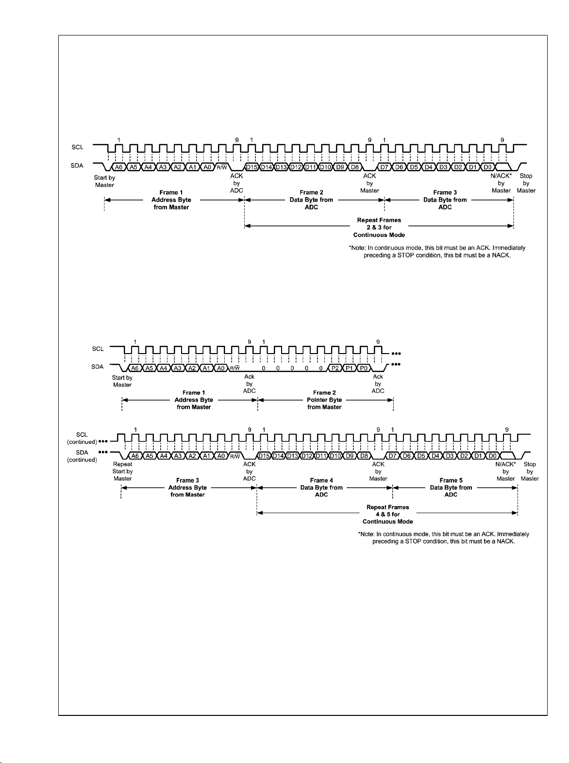
1.10 COMMUNICATING WITH THE ADC101C021
The ADC101C021's data registers are selected by the address pointer (see Section 1.6.1). To read/write a specific data
register, the pointer must be set to that register's address. The
pointer is always written at the beginning of a write operation.
When the pointer needs to be updated for a read cycle, a write
1.10.1 Reading from a 2-Byte ADC Register
ADC101C021/ADC101C027
FIGURE 11. (a) Typical Read from a 2-Byte ADC Register with Preset Pointer
operation must preceed the read operation to set the pointer
address correctly. On the other hand, if the pointer is preset
correctly, a read operation can occur without writing the address pointer register. The following timing diagrams describe
the various read and write operations supported by the ADC.
30052063
30052070
FIGURE 12. (b) Typical Pointer Set Followed by Immediate Read of a 2-Byte ADC Register
www.national.com 24

1.10.2 Reading from a 1-Byte ADC Register
FIGURE 13. (a) Typical Read from a 1-Byte ADC Register with Preset Pointer
ADC101C021/ADC101C027
30052071
30052072
FIGURE 14. (b) Typical Pointer Set Followed by Immediate Read of a 1-Byte ADC Register
25 www.national.com

1.10.3 Writing to an ADC Register
ADC101C021/ADC101C027
30052064
FIGURE 15. (a) Typical Write to a 1-Byte ADC Register
30052073
FIGURE 16. (b) Typical Write to a 2-Byte ADC Register
www.national.com 26

ADC101C021/ADC101C027
1.11 QUIET INTERFACE MODE
To improve performance at High Speed, operate the ADC in
Quiet Interface Mode. This mode provides improved INL and
DNL performance in I2C Hs-Mode (3.4MHz). The Quiet Interface mode provides a maximum throughput rate of 162ksps.
Figure 17 describes how to read the conversion result register
in this mode. Basically, the Master needs to release SCL for
at least 1µs before the MSB of every upper data byte. The
diagram assumes that the address pointer register is set to
its default value.
Quiet Interface mode will only improve INL and DNL performance in Hs-Mode. Standard and Fast mode performance is
unaffected by the Quiet Interface mode.
FIGURE 17. Reading in Quiet Interface Mode
30052076
27 www.national.com
2.0 Applications Information
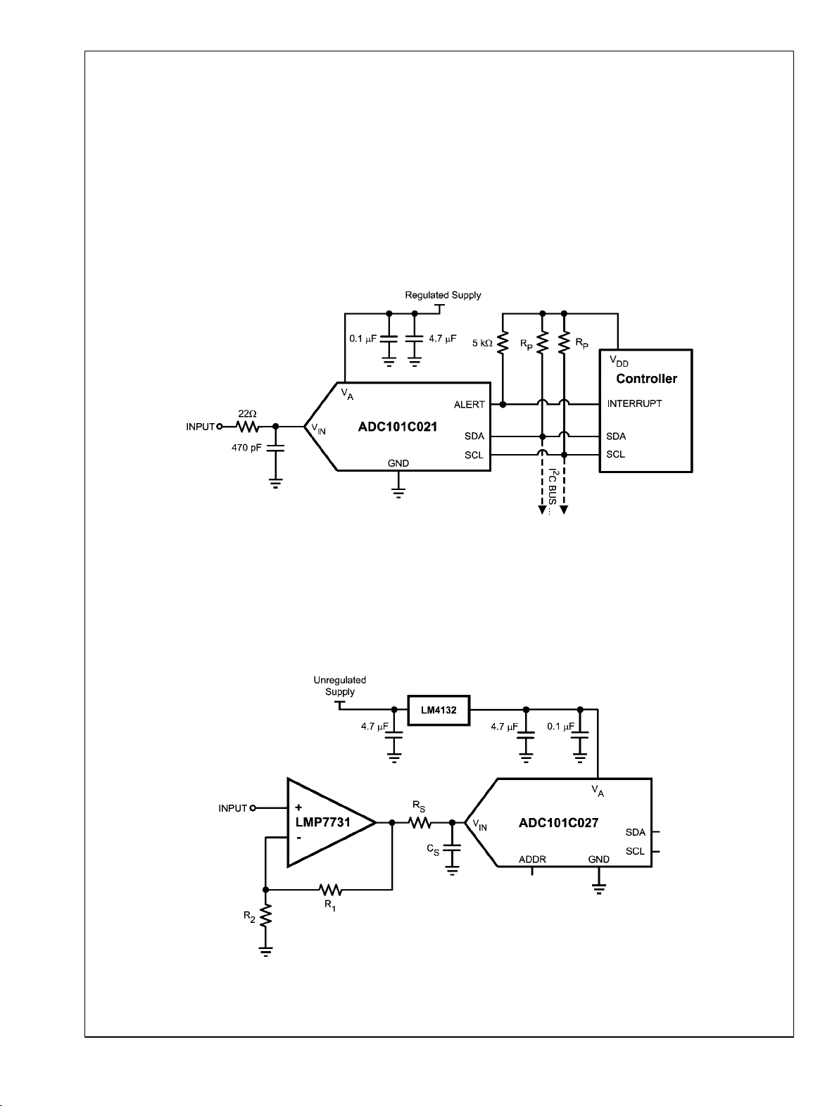
2.1 TYPICAL APPLICATION CIRCUIT
A typical application circuit is shown in Figure 18. The analog
supply is bypassed with a capacitor network located close to
the ADC101C021. The ADC uses the analog supply (VA) as
its reference voltage, so it is very important that VA be kept as
clean as possible. Due to the low power requirements of the
ADC101C021, it is possible to use a precision reference as a
power supply. The pull-up resistors (RP) should be powered
by the controller's supply. It is important that the pull-up resistors are pulled to the same voltage potential VA is set to.
ADC101C021/ADC101C027
This will ensure that the logic levels of all devices on the bus
are compatible. If the controller's supply is noisy, an appro-
priate bypass capacitor should be added between the
controller's supply pin and the pull-up resistors. For Hs-mode
applications, this bypass capacitance will improve the accuracy of the ADC.
The value of the pull-up resistors (RP) depends upon the
characteristics of each particular I2C bus. The I2C specification describes how to choose an appropriate value. As a
general rule-of-thumb, we suggest using a 1kΩ resistor for
Hs-mode bus configurations and a 5kΩ resistor for Standard
or Fast Mode bus configurations. Depending upon the bus
capacitance, these values may not be sufficient to meet the
timing requirements of the I2C bus specification. Please see
the I2C specification for further information.
FIGURE 18. Typical Application Circuit
2.2 BUFFERED INPUT
A bufferred input application circuit is shown in Figure 19. The
analog input is buffered by National's LMP7731. The non-inverting amplifier configuration provides a buffered gain stage
for a single ended source. This application circuit is good for
30052020
single-ended sensor interface. The input must have a DC bias
level that keeps the ADC input signal from swinging below
GND or above the supply (+5V in this case).
The LM4132, with its 0.05% accuracy over temperature, is an
excelent choice as a reference source for the ADC101C021.
FIGURE 19. Buffered Input Circuit
www.national.com 28
30052021

ADC101C021/ADC101C027
2.3 INTELLIGENT BATTERY MONITOR
The ADC101C021 is easily used as an intelligent battery
monitor. The simple circuit shown in Figure 20, uses the
ADC101C021, the LP2980 fixed reference, and a resistor divider to implement an intelligent battery monitor with a window
supervisory feature. The window supervisory feature is implemented by the "out of range" alert function. When the
battery is recharging, the Over Range Alert will indicate that
the charging cycle is complete (see Figure 21). When the
battery is nearing depletion, the Under Range Alert will indicate that the battery is low (see Figure 22).
30052077
In addition to the window supervisory feature, the
ADC101C021 will allow the controller to read the battery voltage at any time during operation. Reading the conversion
result via the I2C interface provides an accurate voltage reading.
The accurate voltage reading and the alert feature will allow
a controller to improve the efficiency of a battery-powered
device. During the discharge cycle, the controller can switch
to a low-battery mode, safely suspend operation, or report a
precise battery level to the user. During the recharge cycle,
the controller can implement an intelligent recharge cycle,
decreasing the charge rate when the battery charge nears
capacity.
2.3.1 Trickle Charge Controller
While a battery is discharging, the ADC101C021 can be used
to control a trickle charge to keep the battery near full capacity
(see Figure 23). When the alert output is active, the battery
will recharge. An intelligent recharge cycle will prevent overcharging and damaging the battery. With a trickle charge, the
battery powered device can be disconnected from the charger
at any time with a full charge.
FIGURE 20. Intelligent Battery Monitor Circuit
FIGURE 21. Recharge Cycle
30052080
FIGURE 23. Trickle Charge
30052078
FIGURE 22. Discharge Cycle
30052079
29 www.national.com

2.4 LAYOUT, GROUNDING, AND BYPASSING
For best accuracy and minimum noise, the printed circuit
board containing the ADC101C021 should have separate
analog and digital areas. The areas are defined by the locations of the analog and digital power planes. Both of these
planes should be located on the same board layer. There
should be a single ground plane. A single, solid ground plane
is preferred if digital return current does not flow through the
analog ground area. Frequently a single ground plane design
will utilize a "fencing" technique to prevent the mixing of analog and digital ground currents. Separate ground planes
should only be utilized when the fencing technique is inade-
ADC101C021/ADC101C027
quate. The separate ground planes must be connected in one
place, preferably near the ADC101C021. Special care is re-
quired to guarantee that signals do not pass over power plane
boundaries. They must always have a continuous return path
below their traces.
The ADC101C021 power supply should be bypassed with a
4.7µF and a 0.1µF capacitor as close as possible to the device
with the 0.1µF right at the device supply pin. The 4.7µF capacitor should be a tantalum type and the 0.1µF capacitor
should be a low ESL type. The power supply for the
ADC101C021 should only be used for analog circuits.
Avoid crossover of analog and digital signals and keep the
clock and data lines on the component side of the board. The
clock and data lines should have controlled impedances.
www.national.com 30

Physical Dimensions inches (millimeters) unless otherwise noted
ADC101C021/ADC101C027
Order Numbers ADC101C021CIMK & ADC101C027CIMK
NS Package Number MK06A
6-Lead TSOT
31 www.national.com

Notes
For more National Semiconductor product information and proven design tools, visit the following Web sites at:
Products Design Support
Amplifiers www.national.com/amplifiers WEBENCH www.national.com/webench
Audio www.national.com/audio Analog University www.national.com/AU
Clock Conditioners www.national.com/timing App Notes www.national.com/appnotes
Data Converters www.national.com/adc Distributors www.national.com/contacts
Displays www.national.com/displays Green Compliance www.national.com/quality/green
Ethernet www.national.com/ethernet Packaging www.national.com/packaging
Interface www.national.com/interface Quality and Reliability www.national.com/quality
LVDS www.national.com/lvds Reference Designs www.national.com/refdesigns
Power Management www.national.com/power Feedback www.national.com/feedback
Switching Regulators www.national.com/switchers
LDOs www.national.com/ldo
LED Lighting www.national.com/led
PowerWise www.national.com/powerwise
Serial Digital Interface (SDI) www.national.com/sdi
Temperature Sensors www.national.com/tempsensors
Wireless (PLL/VCO) www.national.com/wireless
THE CONTENTS OF THIS DOCUMENT ARE PROVIDED IN CONNECTION WITH NATIONAL SEMICONDUCTOR CORPORATION
(“NATIONAL”) PRODUCTS. NATIONAL MAKES NO REPRESENTATIONS OR WARRANTIES WITH RESPECT TO THE ACCURACY
OR COMPLETENESS OF THE CONTENTS OF THIS PUBLICATION AND RESERVES THE RIGHT TO MAKE CHANGES TO
SPECIFICATIONS AND PRODUCT DESCRIPTIONS AT ANY TIME WITHOUT NOTICE. NO LICENSE, WHETHER EXPRESS,
IMPLIED, ARISING BY ESTOPPEL OR OTHERWISE, TO ANY INTELLECTUAL PROPERTY RIGHTS IS GRANTED BY THIS
DOCUMENT.
TESTING AND OTHER QUALITY CONTROLS ARE USED TO THE EXTENT NATIONAL DEEMS NECESSARY TO SUPPORT
NATIONAL’S PRODUCT WARRANTY. EXCEPT WHERE MANDATED BY GOVERNMENT REQUIREMENTS, TESTING OF ALL
PARAMETERS OF EACH PRODUCT IS NOT NECESSARILY PERFORMED. NATIONAL ASSUMES NO LIABILITY FOR
APPLICATIONS ASSISTANCE OR BUYER PRODUCT DESIGN. BUYERS ARE RESPONSIBLE FOR THEIR PRODUCTS AND
APPLICATIONS USING NATIONAL COMPONENTS. PRIOR TO USING OR DISTRIBUTING ANY PRODUCTS THAT INCLUDE
NATIONAL COMPONENTS, BUYERS SHOULD PROVIDE ADEQUATE DESIGN, TESTING AND OPERATING SAFEGUARDS.
EXCEPT AS PROVIDED IN NATIONAL’S TERMS AND CONDITIONS OF SALE FOR SUCH PRODUCTS, NATIONAL ASSUMES NO
LIABILITY WHATSOEVER, AND NATIONAL DISCLAIMS ANY EXPRESS OR IMPLIED WARRANTY RELATING TO THE SALE
AND/OR USE OF NATIONAL PRODUCTS INCLUDING LIABILITY OR WARRANTIES RELATING TO FITNESS FOR A PARTICULAR
C-Compatible, 10-Bit Analog-to-Digital Converter (ADC) with Alert
2
PURPOSE, MERCHANTABILITY, OR INFRINGEMENT OF ANY PATENT, COPYRIGHT OR OTHER INTELLECTUAL PROPERTY
RIGHT.
LIFE SUPPORT POLICY
NATIONAL’S PRODUCTS ARE NOT AUTHORIZED FOR USE AS CRITICAL COMPONENTS IN LIFE SUPPORT DEVICES OR
SYSTEMS WITHOUT THE EXPRESS PRIOR WRITTEN APPROVAL OF THE CHIEF EXECUTIVE OFFICER AND GENERAL
COUNSEL OF NATIONAL SEMICONDUCTOR CORPORATION. As used herein:
Life support devices or systems are devices which (a) are intended for surgical implant into the body, or (b) support or sustain life and
whose failure to perform when properly used in accordance with instructions for use provided in the labeling can be reasonably expected
to result in a significant injury to the user. A critical component is any component in a life support device or system whose failure to perform
can be reasonably expected to cause the failure of the life support device or system or to affect its safety or effectiveness.
National Semiconductor and the National Semiconductor logo are registered trademarks of National Semiconductor Corporation. All other
brand or product names may be trademarks or registered trademarks of their respective holders.
Copyright© 2008 National Semiconductor Corporation
For the most current product information visit us at www.national.com
National Semiconductor
Americas Technical
Support Center
Email: support@nsc.com
ADC101C021/ADC101C027 I
www.national.com
Tel: 1-800-272-9959
National Semiconductor Europe
Technical Support Center
Email: europe.support@nsc.com
German Tel: +49 (0) 180 5010 771
English Tel: +44 (0) 870 850 4288
National Semiconductor Asia
Pacific Technical Support Center
Email: ap.support@nsc.com
National Semiconductor Japan
Technical Support Center
Email: jpn.feedback@nsc.com
 Loading...