

February 8, 2008
ADC08L060
8-Bit, 10 MSPS to 60 MSPS, 0.65 mW/MSPS A/D Converter
with Internal Sample-and-Hold
ADC08L060 8-Bit, 10 MSPS to 60 MSPS, 0.65 mW/MSPS A/D Converter with Internal
Sample-and-Hold
General Description
The ADC08L060 is a low-power, 8-bit, monolithic analog-todigital converter with an on-chip track-and-hold circuit. Optimized for low cost, low power, small size and ease of use, this
product operates at conversion rates of 10 MSPS to
60 MSPS while consuming just 0.65 mW per MHz of clock
frequency, or 39 mW at 60 MSPS. Raising the PD pin puts
the ADC08L060 into a Power Down mode where it consumes
about 1 mW.
The unique architecture achieves 7.6 Effective Bits. The ADC08L060 is resistant to latch-up and the outputs are shortcircuit proof. The top and bottom of the ADC08L060s
reference ladder are available for connections, enabling a
wide range of input possibilities. The digital outputs are TTL/
CMOS compatible with a separate output power supply pin to
support interfacing with 1.8V to 3V logic. The output coding is
straight binary and the digital inputs (CLK and PD) are TTL/
CMOS compatible.
The ADC08L060 is offered in a 24-lead plastic package
(TSSOP) and is specified over the industrial temperature
range of −40°C to +85°C.
Features
Single-ended input
■
Internal sample-and-hold function
■
Low voltage (single +3V) operation
■
Small package
■
Power-down feature
■
Key Specifications
Resolution 8 bits
■
Conversion rate 60 MSPS
■
DNL ±0.25 LSB (typ)
■
INL +0.5/−0.2 LSB (typ)
■
SNR (10.1 MHz) 48 dB (typ)
■
ENOB (10.1 MHz) 7.6 bits (typ)
■
THD (10.1 MHz) −57 dB (typ)
■
Latency 5 Clock Cycles
■
No missing codes Guaranteed
■
Power Consumption
■
Operating 0.65 mW/MSPS (typ)
—
■
Power Down Mode 1.0 mW (typ)
—
Applications
Digital Imaging
■
Set-top boxes
■
Portable Instrumentation
■
Communication Systems
■
X-ray imaging
■
Viterbi decoders
■
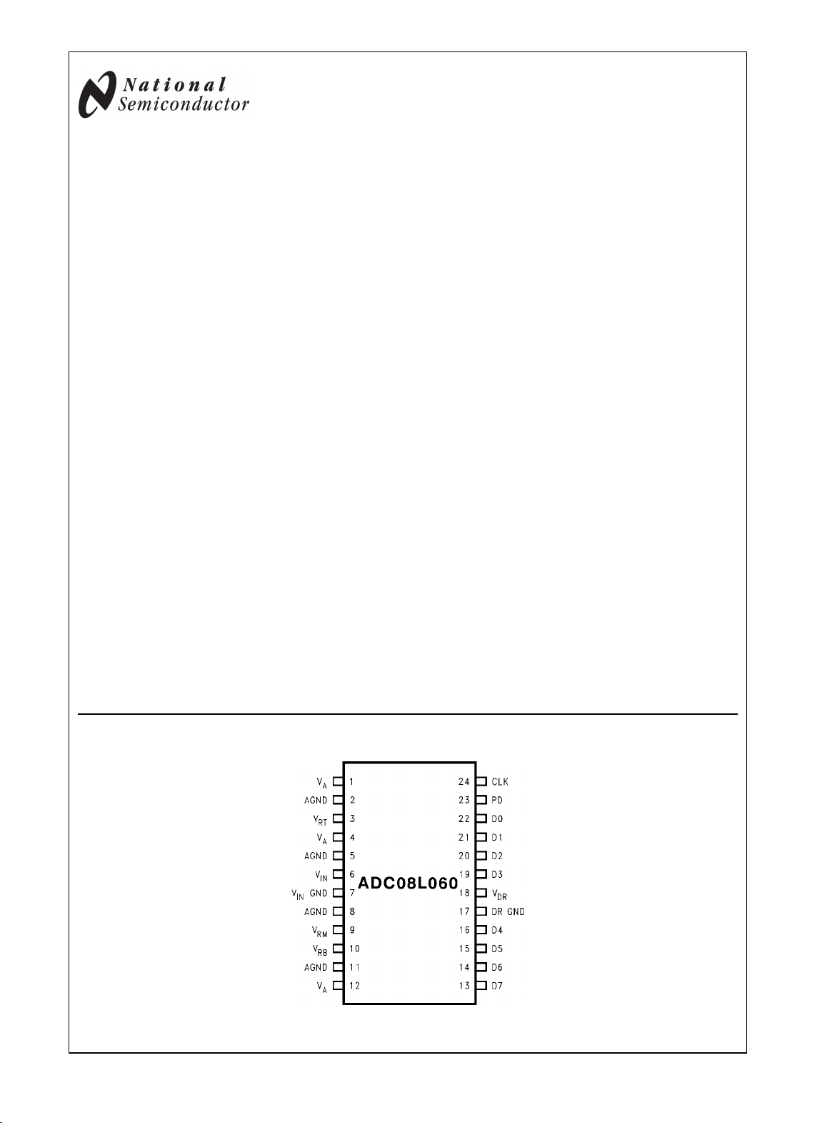
Pin Configuration
20041701
© 2008 National Semiconductor Corporation 200417 www.national.com
Ordering Information
Order Number Temperature Range Package
ADC08L060
ADC08L060CIMT
ADC08L060CIMTX
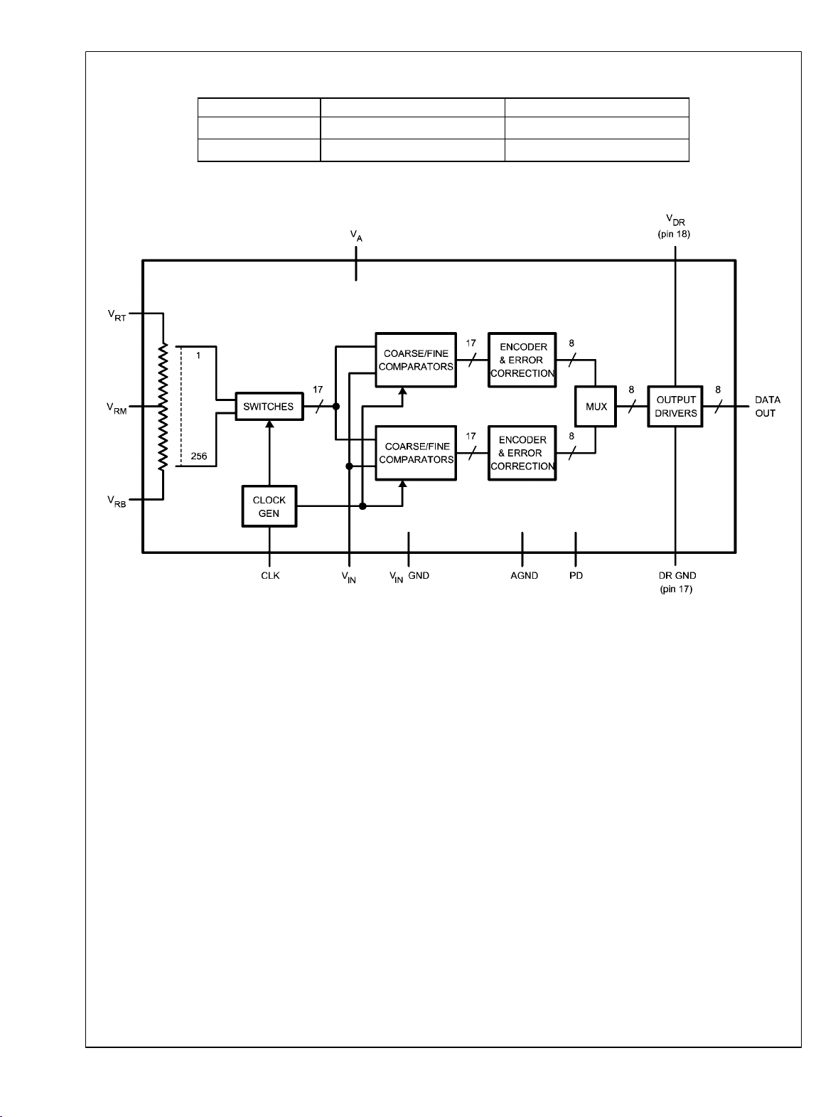
Block Diagram
−40°C ≤ TA ≤ +85°C
−40°C ≤ TA ≤ +85°C
TSSOP
TSSOP (tape and reel)
20041702
www.national.com 2
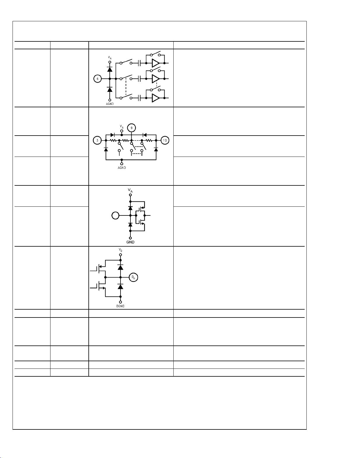
Pin Descriptions and Equivalent Circuits
Pin No. Symbol Equivalent Circuit Description
ADC08L060
6
3
9
10
V
IN
V
RT
V
RM
V
RB
23 PD
24 CLK
Analog signal input. Conversion range is VRB to VRT.
Analog Input that is the high (top) side of the reference ladder
of the ADC. Nominal range is 0.5V to VA. Voltage on VRT and
VRB inputs define the VIN conversion range. Bypass well. See
Section 2.0 for more information.
Mid-point of the reference ladder. This pin should be
bypassed to a quiet point in the analog ground plane with a
0.1 µF capacitor.
Analog Input that is the low side (bottom) of the reference
ladder of the ADC. Nominal range is 0.0V to (VRT – 0.5V).
Voltage on VRT and VRB inputs define the VIN conversion
range. Bypass well. See Section 2.0 for more information.
Power Down input. When this pin is high, the converter is in
the Power Down mode and the data output pins hold the last
conversion result.
CMOS/TTL compatible digital clock Input. VIN is sampled on
the rising edge of CLK input.
13 thru 16
and
19 thru 22
7
D0–D7
VIN GND
Conversion data digital Output pins. D0 is the LSB, D7 is the
MSB. Valid data is output after the rising edge of the CLK
input.
Reference ground for the single-ended analog input, VIN.
Positive analog supply pin. Connect to a quiet voltage source
1, 4, 12
V
A
of +3V. VA should be bypassed with a 0.1 µF ceramic chip
capacitor for each pin, plus one 10 µF capacitor. See Section
3.0 for more information.
18
V
DR
Power supply for the output drivers. If connected to VA,
decouple well from VA.
17 DR GND The ground return for the output driver supply.
2, 5, 8, 11 AGND The ground return for the analog supply.
3 www.national.com
Absolute Maximum Ratings
(Notes 1, 2)
If Military/Aerospace specified devices are required,
ADC08L060
please contact the National Semiconductor Sales Office/
Distributors for availability and specifications.
Supply Voltage (VA)
Driver Supply Voltage (VDR) VA +0.3V
Voltage on Any Input or Output Pin −0.3V to V
Reference Voltage (VRT, VRB) VA to AGND
3.8V
A
Operating Ratings (Notes 1, 2)
Operating Temperature Range
Supply Voltage, V
Driver Supply Voltage, V
Output Driver Voltage, V
A
DR
DR
Ground Difference |GND − DR GND| 0V to 300 mV
Upper Reference Voltage (VRT) 0.5V to (VA −0.3V)
Lower Reference Voltage (VRB) 0V to (VRT −0.5V)
VIN Voltage Range VRB to V
−40°C ≤ TA ≤ +85°C
+2.4V to +3.6V
+2.4V to V
1.8V to V
CLK, PD Voltage Range −0.05V to
(VA + 0.05V)
Input Current at Any Pin (Note 3) ±25 mA
Package Input Current (Note 3) ±50 mA
Power Dissipation at TA = 25°C
ESD Susceptibility (Note 6)
Human Body Model
Machine Model
See (Note 5)
2500V
200V
Package Thermal Resistance
Package
24-Lead TSSOP 92°C/W
θ
JA
Soldering Temperature, Infrared,
10 seconds (Note 7) 235°C
Storage Temperature −65°C to +150°C
Converter Electrical Characteristics
The following specifications apply for VA = VDR = +3.0VDC, VRT = +1.9V, VRB = 0.3V, CL = 10 pF, f
Boldface limits apply for TJ = T
Symbol Parameter Conditions
MIN
to T
: all other limits TJ = 25°C (Notes 4, 8, 9)
MAX
(Note 10)
DC ACCURACY
INL Integral Non-Linearity
DNL Differential Non-Linearity ±0.25 ±0.90 LSB (max)
Missing Codes 0 (max)
FSE Full Scale Error 3.0 ±13 mV (max)
V
OFF
Zero Scale Offset Error 19 27 mV (max)
ANALOG INPUT AND REFERENCE CHARACTERISTICS
V
IN
C
IN
R
IN
Input Voltage 1.6
VIN Input Capacitance VIN = 0.75V +0.5 Vrms
RIN Input Resistance
>1
(CLK LOW) 3 pF
(CLK HIGH) 4 pF
BW Full Power Bandwidth 270 MHz
V
RT
V
RB
VRT - V
R
REF
I
ref
Top Reference Voltage
Bottom Reference Voltage
Reference Delta 1.6
RB
Reference Ladder Resistance
Reference Ladder Current
VRT to V
VRT to V
RB
RB
= 60 MHz at 50% duty cycle.
CLK
Typical
Limits
(Note 10)
+0.5
−0.2
1.9
0.3
+1.9
−1.35
V
RB
V
RT
V
A
0.5 V (min)
VRT − 0.5
0 V (min)
2.3 V (max)
1.0 V (min)
720
2.2
590
1070
1.5 mA (min)
2.7 mA (max)
(Limits)
LSB (max)
LSB (min)
V (max)
V (max)
V (max)
Ω (max)
A
A
RT
Units
V (min)
MΩ
Ω (min)
www.national.com 4

ADC08L060
Symbol Parameter Conditions
CLK, PD DIGITAL INPUT CHARACTERISTICS
V
IH
V
IL
I
IH
I
IL
C
IN
Logical High Input Voltage
Logical Low Input Voltage
Logical High Input Current
Logical Low Input Current
Logic Input Capacitance 3 pF
VDR = VA = 3.6V
VDR = VA = 2.7V
VIH = VDR = VA = 3.6V
VIL = 0V, VDR = VA = 2.7V
DIGITAL OUTPUT CHARACTERISTICS
V
OH
V
OL
High Level Output Voltage
Low Level Output Voltage
VA = VDR = 2.7V, IOH = −400 µA
VA = VDR = 2.7V, IOL = 1.0 mA
DYNAMIC PERFORMANCE
ENOB Effective Number of Bits
SINAD Signal-to-Noise & Distortion
SNR Signal-to-Noise Ratio
SFDR Spurious Free Dynamic Range
THD Total Harmonic Distortion
HD2 2nd Harmonic Distortion
HD3 3rd Harmonic Distortion
IMD Intermodulation Distortion
fIN = 10.1 MHz, VIN = FS − 0.25 dB
fIN = 29 MHz, VIN = FS − 0.25 dB
fIN = 10.1 MHz, VIN = FS − 0.25 dB
fIN = 29 MHz, VIN = FS − 0.25 dB
fIN = 10.1 MHz, VIN = FS − 0.25 dB
fIN = 29 MHz, VIN = FS − 0.25 dB
fIN = 10.1 MHz, VIN = FS − 0.25 dB
fIN = 29 MHz, VIN = FS − 0.25 dB
fIN = 10.1 MHz, VIN = FS − 0.25 dB
fIN = 29 MHz, VIN = FS − 0.25 dB
fIN = 10.1 MHz, VIN = FS − 0.25 dB
fIN = 29 MHz, VIN = FS − 0.25 dB
fIN = 10.1 MHz, VIN = FS − 0.25 dB
fIN = 29 MHz, VIN = FS − 0.25 dB
f1 = 11 MHz, VIN = FS − 6.25 dB
f2 = 12 MHz, VIN = FS − 6.25 dB
POWER SUPPLY CHARACTERISTICS
I
A
DRI
Analog Supply Current
Output Driver Supply Current
D
DC Input 13 15.9 mA (max)
fIN = 10 MHz, VIN = FS − 3 dB
DC Input 0.04 0.2 mA (max)
fIN = 10 MHz, VIN = FS − 3 dB (Note 11)
DC Input 13 16.1 mA (max)
IA + DRI
Total Operating Current
D
fIN = 10 MHz, VIN = FS − 3 dB, PD = Low
CLK Low, PD = Hi 0.33 mA
DC Input 39 48.3 mW (max)
PC Power Consumption
fIN = 10 MHz, VIN = FS − 3 dB, PD = Low
CLK Low, PD = Hi 1 mW
PSRR
PSRR
Power Supply Rejection Ratio
1
Power Supply Rejection Ratio
2
FSE change with 2.7V to 3.3V change in
V
A
SNR reduction with 200 mV at 1MHz on
supply
Typical
(Note 10)
Limits
(Note 10)
(Limits)
2.0 V (min)
0.8 V (max)
10 nA
−50 nA
2.6 2.4 V (min)
0.4 0.5 V (max)
7.6 6.9 Bits (min)
7.4 Bits
47.4 43.3 dB (min)
46.1 dB
48
44.5
dB (min)
47.2 dB
59.1
54.5 dBc
−56.9
−53.3 dBc
-61.1 dBc
−54.9 dBc
−64.2 dBc
−63.1 dBc
−55 dBc
14
4.2 mA
18.2 mA
53
−51 dB
45 dB
Units
dBc
dBc
mA
mW
5 www.national.com
Symbol Parameter Conditions
Typical
(Note 10)
Limits
(Note 10)
(Limits)
AC ELECTRICAL CHARACTERISTICS
f
C1
ADC08L060
f
C2
t
CL
t
CH
DC Clock Duty Cycle
t
OH
t
OD
Maximum Conversion Rate 80 60 MHz (min)
Minimum Conversion Rate 10 MHz
Minimum Clock Low Time 0.62 ns (min)
Minimum Clock High Time 0.62 ns (min)
95
5
%(min)
%(max)
Output Hold Time CLK to Data Invalid 5.2 ns
Output Delay CLK to Data Transition 7.1
5.0 ns (min)
9.4 ns (max)
Pipeline Delay (Latency) 5 Clock Cycles
t
AD
t
AJ
Note 1: Absolute Maximum Ratings indicate limits beyond which damage to the device may occur, including inoperability and degradation of device reliability
and/or performance. Functional operation of the device and/or non-degradation at the Absolute Maximum Ratings or other conditions beyond those indicated in
the Recommended Operating Conditions is not implied. The recommended Operating Conditions indicate conditions at which the device is functional and the
device should not be operated beyond such conditions..
Note 2: All voltages are measured with respect to GND = AGND = DR GND = 0V, unless otherwise specified.
Note 3: When the input voltage at any pin exceeds the power supplies (that is, less than AGND or DR GND, or greater than VA or VDR), the current at that pin
should be limited to 25 mA. The 50 mA maximum package input current rating limits the number of pins that can safely exceed the power supplies with an input
current of 25 mA to two.
Note 4: The Electrical characteristics tables list guaranteed specifications under the listed Recommended Conditions except as otherwise modified or specified
by the Electrical Characteristics Conditions and/or Notes. Typical specifications are estimations for room temperature only and are not guaranteed.
Note 5: The absolute maximum junction temperature (TJmax) for this device is 150°C. The maximum allowable power dissipation is dictated by TJmax, the
junction-to-ambient thermal resistance (θJA), and the ambient temperature (TA), and can be calculated using the formula PDMAX = (TJmax − TA) / θJA. The values
for maximum power dissipation will be reached only when this device is operated in a severe fault condition (e.g., when input or output pins are driven beyond
the power supply voltages, or the power supply polarity is reversed). Obviously, such conditions should always be avoided.
Note 6: Human body model is 100 pF capacitor discharged through a 1.5 kΩ resistor. Machine model is 220 pF discharged through ZERO Ohms.
Note 7: See AN-450, “Surface Mounting Methods and Their Effect on Product Reliability”.
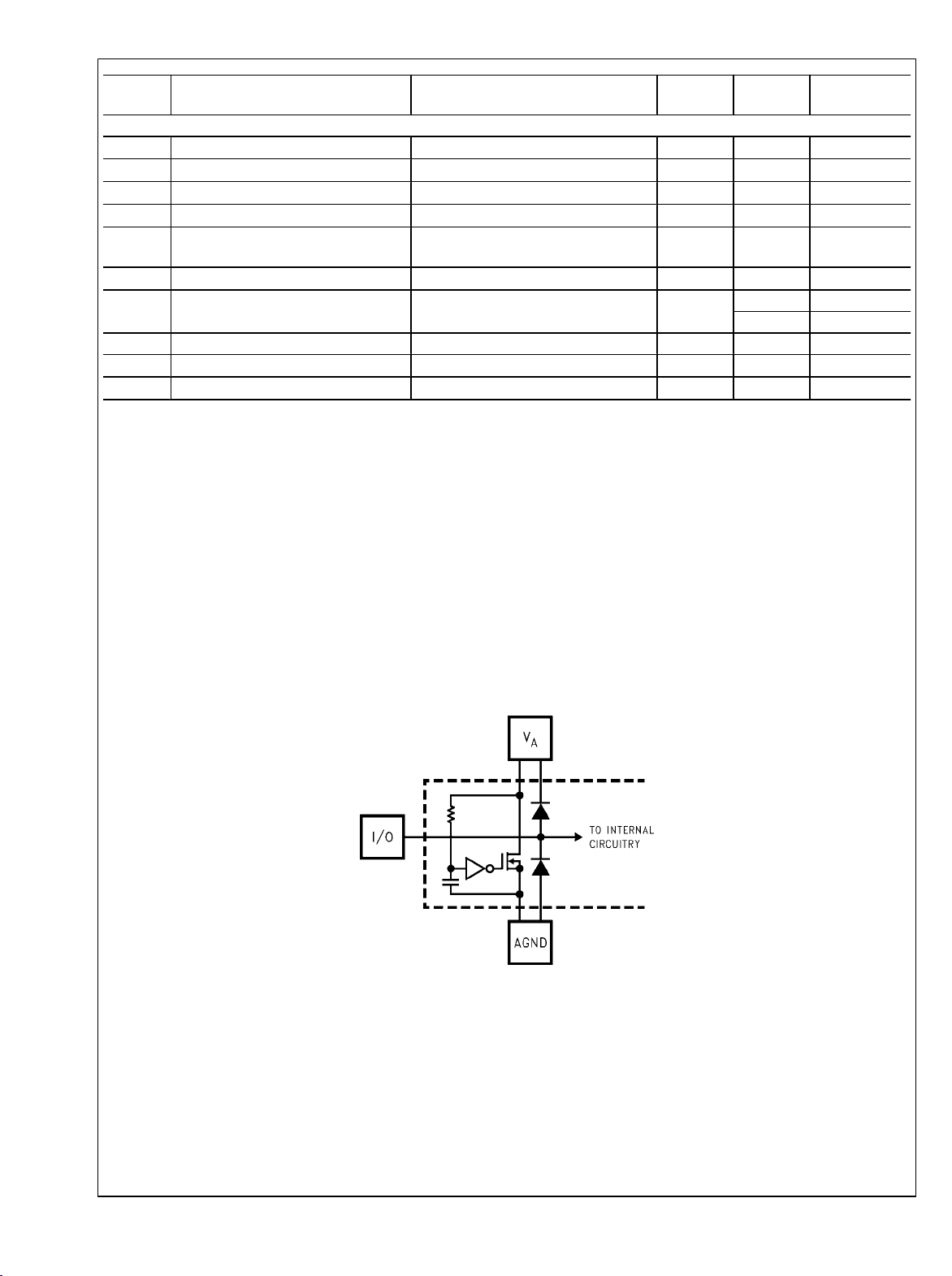
Note 8: The analog inputs are protected as shown below. Input voltage magnitudes up to VA + 300 mV or to 300 mV below GND will not damage this device.
However, errors in the A/D conversion can occur if the input goes above VDR or below GND by more than 100 mV. For example, if VA is 2.7VDC the full-scale
input voltage must be ≤2.8VDC to ensure accurate conversions.
Sampling (Aperture) Delay CLK Rise to Acquisition of Data 2.6 ns
Aperture Jitter 2 ps rms
Units
20041707
Note 9: To guarantee accuracy, it is required that VA and VDR be well bypassed. Each supply pin must be decoupled with separate bypass capacitors.
Note 10: Typical figures are at TJ = 25°C, and represent most likely parametric norms at specific conditions at the time of product characterization and are not
guaranteed. Test limits are guaranteed to National's AOQL (Average Outgoing Quality Level).
Note 11: IDR is the current consumed by the switching of the output drivers and is primarily determined by the load capacitance on the output pins, the supply
voltage, VDR, and the rate at which the outputs are switching (which is signal dependent), IDR = VDR (CO x fO + C1 x f1 + … + C71 x f7) where VDR is the output
driver power supply voltage, Cn is the total capacitance on any given output pin, and fn is the average frequency at which that pin is toggling.
www.national.com 6
 Loading...