

National Semiconductor ADC102S051, ADC082S051, ADC122S051, ADC122S021, ADC082S021 User Manual
...Page 1
National Semiconductor
Evaluation Board User's Guide
12-, 10- and 8-Bit General Purpose
Analog-to-Digital Converters with Input Multiplexer
ADC122S101 / ADC102S101 / ADC082S101
ADC122S051 / ADC102S051 / ADC082S051
ADC122S021 / ADC102S021 / ADC082S021
ADC124S101 / ADC104S101 / ADC084S101
ADC124S051 / ADC104S051 / ADC084S051
ADC124S021 / ADC104S021 / ADC084S021
August 2005
Rev -
© 2005 National Semiconductor Corporation.
1 http://www.national.com
Page 2

Table of Contents
1.0 Introduction.............................................................................................................................3
2.0 Board Assembly .....................................................................................................................3
3.0 Quick Start..............................................................................................................................3
4.0 Functional Description............................................................................................................4
4.1 Input (signal conditioning) circuitry............................................................................4
4.2 The ADC reference ...................................................................................................4
4.3 ADC clock circuit .......................................................................................................4
4.5 Digital Data Output....................................................................................................4
4.6 Power Supply Connections .......................................................................................4
4.7 Power Requirements.................................................................................................5
4.8 Analog Inputs ............................................................................................................5
5.0 Installing and Using the ADCxx1S101 Evaluation Board .......................................................5
5.1 Software Installation..................................................................................................5
5.2 Setting up the ADCxx1S101 Evaluation Board .........................................................5
5.2.1 Board Set-up .............................................................................................5
5.2.2 Quick Check of Analog Functions.............................................................5
5.2.3 Quick Check of Software and Computer Interface Operation...................5
5.2.4 Getting Consistent Readings.....................................................................6
5.2.5 Troubleshooting.........................................................................................6
6.0 Evaluation Board Specifications.............................................................................................6
7.0 Hardware Schematic..............................................................................................................7
8.0 ADCxx1S101 Evaluation Board Bill of Materials ....................................................................8
A1 Summary Tables of Test Points and Connectors ...................................................................9
2 http://www.national.com
Page 3

1.0 Introduction
These ADC Design Kits (consisting of one of these
evaluation boards: ADC12xS101, ADC10xS101,
ADC08xS101, ADC12xS051, ADC10xS051,
ADC08xS051, ADC12xS021, ADC10xS021,
ADC08xS021 and WaveVision4 hardware, where "x" in
the device types here could be a 2 or a 4, indicating the
number of multiplexer inputs) is designed to ease
evaluation and design-in of these National
Semiconductor Analog-to-Digital Converters. These
evaluation boards allow the desivgner to evaluate product
performance in a choice of two ways: in standalone mode
with a logic analyzer and appropriate software (including
National's WaveVision software), or with a personal
computer and WaveVision4 hardware and software.
Reference in this Guide to DUT is meant to refer to the
particular device for which you have the evaluation board.
For operation with a computer system, this evaluation
board should be coupled to a WaveVision4 data capture
board (National part number WAVEVSN BRD 4.0) using
the WaveVision software operating under Microsoft
Windows. The analog signal presented to the DUT is
captured by the WaveVision4 data capture board, and
displayed on the computer screen as a dynamic
waveform, FFT, and/or histogram. The software also
computes and displays dynamic performance in the form
of SNR, SINAD, THD, SFDR, and ENOB.
Important Note: The evaluation boards for all of these ADCs
look identical. The actual device placed on your evaluation
board can be identified by the label on the board and verified
by looking at the DUT (Device Under Test) top mark. The
devices have the following top marks:
Device Top Mark
ADC082S101 X22C
ADC082S051 X04C
ADC082S021 X16C
ADC084S101 X25C
ADC084S051 X10C 8. Run the WaveVision 4 software and click on
ADC084S021 X19C
ADC102S101 X23C
ADC102S051 X05C
ADC102S021 X17C
ADC104S101 X26C
ADC104S051 X11C
ADC104S021 X20C
ADC122S101 X24C
ADC122S051 X06C
ADC122S021 X18C
ADC124S101 X27C
ADC124S051 X12C
ADC124S021 X21C
The signal at the Analog Input to the board is digitized
and is available at FutureBus connector J2.
The board inputs are provided at BNC1 and BNC2.
Jumper headers JP1 and JP3 allow these inputs to be
either a.c. or d.c. coupled to the DUT. Provision is made
to adjust the DUT supply voltage (measured at TP1) with
potentiometer VR1.
VR2 is used to set the input offset.
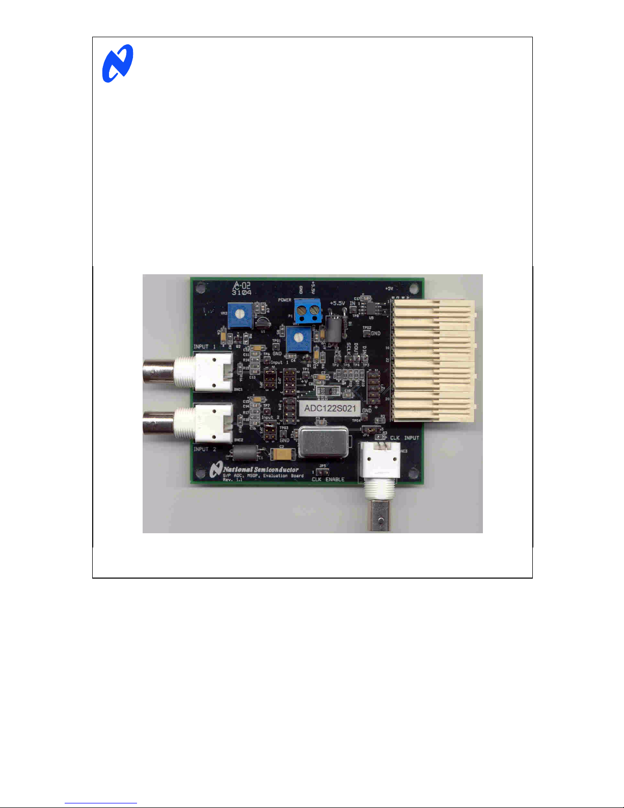
2.0 Board Assembly
These Evaluation Boards come fully assembled and
ready to use. Refer to the Bill of Materials for a
description of components, to Figure 1 for major
component placement and to Figure 2 for the Evaluation
Board schematic.
3.0 Quick Start
Refer to Figure 1 for locations of test points and major
components.
1. Connect the evaluation board to the Capture Board
(order number WAVEVSN BRD 4.0). See the
Capture Board Manual for operation of that board.
2. Connect a clean power supply to the terminals of
connector P1. Adjust power supply to a voltage of
±5.5V to ±5.7V before connecting it to the board.
3. Connect a voltmeter to TP1 and use VR1 to set the
DUT analog supply voltage for the desired value
between +2.7V and +5.0V.
4. Set the jumper to short pins 1 and 2 of JP6 and be
sure there is a clock oscillator of the appropriate
frequency at Y1.
5. Put a jumper between pins 1 and 2 of JP1 and pins
1 and 2 of JP2.
6. Connect a signal, through an appropriate bandpass
filter, to BNC1. The peak-to-peak amplitude of this
signal at TP6 should be the same as or just under
the power supply voltage setting.
7. Connect a USB cable between the WaveVision
Capture Board and the PC.
Settings, then click on Capture. Under "Board Type"
select "WaveVision 4.0 (USB)".
9. Under "Communication" press the "Test" button. If
you get a "Communication Failed" message, check
all connections and be sure the power supply is on.
10. If the appropriate sample rate (not clock rate) is not
reported, check to be sure the clock signal has
adequate amplitude and repeat the previous step.
11. Click "Accept" then gather data by pressing F1 on
the keyboard. Perform an FFT on the data by
clicking on the FFT tab.
See the WaveVision Capture Board Manual for complete
data gathering instructions.
3 http://www.national.com
Page 4
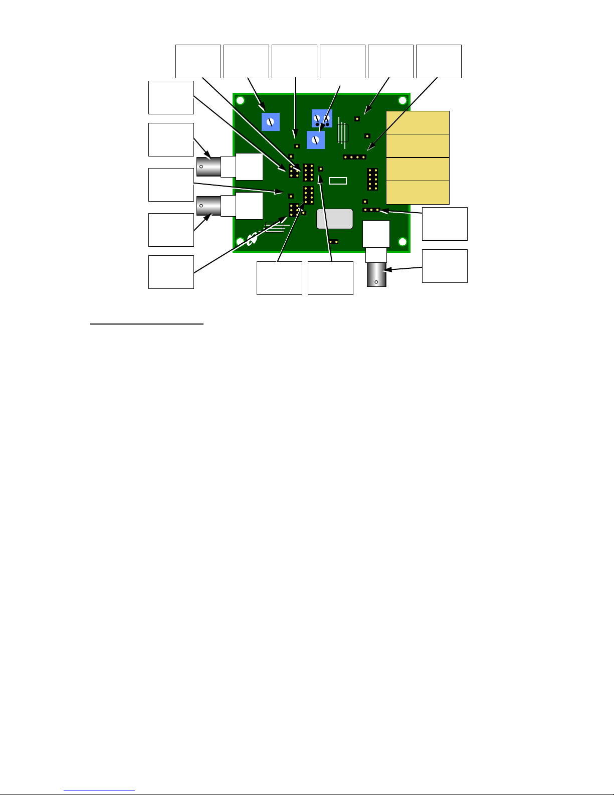
Input 1 Chan
JP1
INPUT 1
AC/DC Couple
BNC1
INPUT 1
Connection
JP2
Select
VR2
Offset
Adjust
INPUT 1
INPUT 1
Test Point
VR2
TP6
BNC1
TP7
INPUT 2
Test Point
BNC1
JP1
BNC2
JP3
BNC2
INPUT 2
Connection
JP3
INPUT 2
AC/DC Couple
BNC2
INPUT 2
National Semiconductor
G/P ADC, MSOP, Evaluation Board
Rev. 1.1
Input 1 Chan
L1
JP2
Select
Figure 1. Major Components and Test Points of the Evaluation Board
4.0 Functional Description
The Evaluation Board component locations are shown in
Figure 1. The board schematic is shown in Figure 2.
4.1 Input (signal conditioning) circuitry
The input signal to be digitized should be applied to BNC
connector BNC1 or to BNC2, or to both through (an)
appropriate filter(s). These 50 Ohm inputs are intended to
accept a low-noise sine wave signal of peak-to-peak
amplitude up to the power supply level. To accurately
evaluate the ADC dynamic performance, the input test
signal should be a single frequency passed through a
high-quality band pass filter as described in Section 5.0.
The input signal may be either a.c. or d.c. coupled to the
DUT with the setting of jumpers on J1 and JP3. See
schematic Figure 2.
4.2 The ADC reference
The reference voltage for the DUT is the device supply
voltage. Therefore, adjusting this voltage will change the
full scale range of the DUT. Since the operational supply
voltage range of the these ADCs is 2.7V to 5.25V, this is
also the range of the reference voltage.
TP6
TP7
Input2
TPG1
GND
POWER
Input1
JP2
JP4
TPG3
GND
P1
VR1
VA Supply
TP1
+V
U2, U3, U4
JP5
JP6
Clock
Select
VR1
Adjust
L2
TP2 TP5 TP4 TP3
Y1
+5.5V IN 1
TP8
TPG4
+5.5V Input
TPG2
GND
GND
JP6
BNC3
TP8
Test Point
J2
LA1
CLK INPUT
BNC3
TP2, TP3,
TP4, TP5
Serial Lines
Test Points
JP6
Clock
Select
BNC3
Ext. Clock
Connection
4.3 ADC Input Bias
To maximize ADC performance it is necessary that the
input signal swing cover nearly the entire ADC input
range. If the input biasing is not at the center of the signal
swing, it will not be possible to get maximum signal swing
without clipping of the signal, at which point there will be
excessive distortion.
VR2 is provided to allow adjustment of the input bias
point when a.c. input coupling is used. VR2 should be
adjusted to provide a d.c. voltage at TP6 and TP7 that
are one half the DUT supply voltage at TP1.
4.4 ADC clock circuit
The clock signal applied to the ADC can come from
BNC3 or from an on-board oscillator at position Y1 or Y2.
Y1 is for a through-hole TTL oscillator, while Y2 is for a
surface mounted TTL oscillator. Only one oscillator
should be mounted at a time and either an oscillator or
an external generator should be connected. JP6 is used
to select the oscillator source. Shorting pins 1 and 2 of
JP6 selects the on-board oscillator, while shorting pins 2
and 3 selects the oscillator signal at BNC3.
4 http://www.national.com
Page 5

4.5 Digital Data Output.
The digital output data from the DUT is available at
Header LA1 for connection to a logic analyzer. Data is
transferred over FutureBus J5 for use with the
WaveVision4 data capture board.
4.6 Power Supply Connections
Power to this board is supplied through power connector
J6. The only Voltage needed for the evaluation board is a
single +5.5V to +5.7V supply.
When using this evaluation Board with the WaveVision4
Capture Board, the +5V logic power supply for that
Capture board and the +5V of the DUT evaluation board
are connected together through pins A1, B1, A2 and B2
of J2. Diode D1 between P1 and the WaveVision4 board
is meant to prevent the higher voltage at DUT board P1
from getting to the WaveVision4 board. Providing the
+5.5V to +5.7V to the DUT board will provide +5V to the
WaveVision4 board through D1 and the WaveVision4
board pins A1, B1, A2 and B2 of J2.
4.7 Power Requirements
Voltage and current requirements for the DUT Evaluation
Board are
• Pin 1 of P1: +5.5V to 5.7V at 50 mA
• Pin 2 of P1: Ground
4.8 Analog Inputs
The evaluation board input channel is composed of
termination components and a user choice of a.c. or d.c.
signal coupling to the DUT, as well as a choice of DUT
multiplexer inputs that are connected to inputs BNC1 and
BNC2. Short together pins 1 and 2 of JP1 and JP3 to a.c.
couple the input signals. Short pins 5 and 6 of JP1 and
JP3 to d.c. couple the input signal to the DUT. Shorting
together pins 3 and 4 of JP1 or JP3 will ground the
corresponding ADC input.
JP2 and JP4 determine which BNC connector is
connected to which ADC input. See Figure 2 for the
device schematic.
Caution: Be sure that the input signals to the DUT do
not go more negative than -0.3V or more than 0.3V
above the DUT power supply.
5.0 Installing and Using the ADCxx1S101
Evaluation Board
The evaluation board requires a power supply as
described in Section 4.7. An appropriate signal generator
with 50 Ohm source impedance should be connected to
the Analog Input BNC1 and/or BNC2. A bandpass filter
should be inserted between the generator output and the
input to the evaluation board when evaluating sinusoidal
signals to be sure there are no unwanted frequencies
(harmonics and noise) presented to the ADC. It is
important to realize that no frequency generator or
synthesizer produces a pure enough sine wave to
evaluate an A/D Converter without the use of a good
filter. If the WaveVison4 capture board is used, a USB
cable must be connected between the WaveVision4
Capture Board and the host computer. See the
WaveVision4 Capture Board User's Guide for details.
5.1 Software Installation
The WaveVision4 software provided requires about 6
Megabytes of hard drive space, including the Java files,
and runs under Windows. See the WaveVision4 Capture
Board Users' Guide for WaveVision4 software installation
instructions.
5.2 Setting up the Evaluation Board
This evaluation package was designed to be easy and
simple to use, and to provide a quick and simple way to
evaluate the DUT. The procedures given here will help
you to properly set up the board.
5.2.1 Board Set-up
Refer to Figure 1 for locations of the major components
on the board.
1. Connect The evaluation board to a WaveVision4
Capture Board, WAVEVSN BRD 4.0.
2. Connect the desired jumper to JP1, JP2, JP3 and
JP4. (See Section 4.8).
3. Connect power to the board per requirements of
paragraph 4.7.
4. Connect a USB cable between the WaveVision4
Capture Board and a USB port on your computer.
5. Connect a clean power supply to the terminals of
connector P1. Adjust power supply to a voltage of
±5.5V to ±5.7V before connecting it to the board.
Apply power to the WaveVision4 Capture Board.
6. Connect an appropriate test signal source to
connector BNC1 and/or BNC2 of the evaluation
board through (an) appropriate filter(s).
5.2.2 Quick Check of Analog Functions
Refer to Figure 1 for locations of major components on
the board. If at any time the expected response is not
obtained, see section 5.2.5 on Troubleshooting.
1. Perform steps 1 through 6 of Section 5.2.1.
2. Adjust VR1 for the desired DUT supply voltage at
TP1.
3. Adjust VR2 for a voltage at TP6 and TP7 that are
1/2 that at TP1.
4. Apply a signal to BNC1 and scope TP6 to be sure
the input signal is present.
5. Apply a signal to BNC2 and scope TP7 to be sure
the input signal is present.
5 http://www.national.com
Page 6

This completes the testing of the analog portion of the
evaluation board.
5.2.3 Quick Check of Software and Computer
Interface Operation
1. Perform the steps of Paragraph 5.2.2, above.
2. Put a jumper between pins 1 and 2 of JP1 and
between pins 1 and 2 of JP2.
3. Apply a signal to BNC1. Adjust the signal source at
Analog Input BNC1 for a peak-to-peak signal
amplitude at TP6 that is very slightly below the value
of the d.c. voltage at TP1.
4. Be sure there is an interconnecting cable between
the Capture Board and your computer USB port.
5. Run the WaveVision4 program and click on
Settings, then click on Capture. Under "Board Type"
select "WaveVision 4.0 (USB)".
6. Under "Communication" press the "Test" button. If
you get a "Communication Failed" message, test all
connections and be sure the power supply to the
boards is turned on. Click on "Accept".
7. Acquire data by pressing the computer F1 key. Data
transfer can take a few seconds.
8. When transfer is complete, the data window should
show many sine waves. The display may show a
nearly solid area of red, which is O.K.
9. With the mouse, you may click on the magnifying
glass, then and drag (top left to bottom right) to
select a portion of the displayed waveform for better
examination.
10. Click on the FFT tab to compute the FFT and
display a frequency domain plot.
The FFT data will provide a measurement of SINAD,
SNR, THD SFDR and ENOB, simplifying the
performance verification of the DUT.
Note: Be sure to use a band pass filter between the
signal source and this board for accurate dynamic
performance measurement.
To change the selected input channel, click on the
"Settings" pull-down, then on "Product Board Settings"
and choose the selected channel. Choosing "GND" will
internally ground the ADC input. It is necessary to select
the mainWaveVision4 window before capturing data.
5.2.4 Getting Consistent Readings
Artifacts can result when we perform an FFT on a
digitized waveform, producing inconsistent results when
testing repeatedly. The presence of these artifacts means
that the ADC under test may perform better than our
measurements would indicate. Windowing is a common
method of improving FFT results of finite data.
We can eliminate the need for windowing and get more
consistent results if we observe the proper ratios between
the input and sampling frequencies, forcing the data to
cleanly "wrap around" itself, providing coherent sampling.
This eliminates the distortion that would otherwise be
present in an FFT and greatly increases its spectral
resolution. This, in turn, allows us to more accurately
evaluate the spectral response of the A/D converter.
When we do this, however, we must be sure that the
input signal has high spectral purity and stability and that
the sampling clock signal is extremely stable with
minimal jitter.
Coherent sampling of a periodic waveform occurs when
an integer number of cycles exists in the sample window.
The relationship between the number of cycles sampled
(CY), the number of samples taken (SS), the signal input
frequency (fin) and the sample rate (fs), for coherent
sampling, is
f
CY
in
=
f
SS
s
CY, the number of cycles in the data record, must be a
prime integer number and SS, the number of samples in
the record, must be a power of 2 integer.
Further, fin (signal input frequency) and fs (sampling rate)
should be locked to each other. Then, if they come from
the same generator, whatever frequency instability (jitter)
is present in the two signals will cancel each other.
Windowing (an FFT Option under WaveVision) should
not be used for coherent sampling.
5.2.5 Troubleshooting
Nothing happens when F1 is pressed
then Capture Board Settings and look at the top for
"Board Properties" If you see "No WaveVision hardware
is present", be sure that the WaveVision Capture Board
is connected to an USB port and has power, that the
evaluation board has power and is properly connected to
and seated with the WaveVision4 Capture Board.
There is no output from the DUT: perform the following:
: Select Settings,
• Be sure the appropriate input channel is selected
through the WaveVision4 software.
• Be sure that a shorting jumper is appropriately
placed on JP1 through JP4.
• Be sure that the proper voltage and polarity is
present at Power Connector J6.
• Check to see that the DUT input signal does not go
below ground or above the DUT supply voltage.
• Be sure there is a clock signal is present at TP5.
The PC displayed waveform appears to be noisy, or the
FFT plot shows nothing but noise with no apparent
signal:
• Be sure the appropriate input channel is selected
through the WaveVision4 software.
• Be sure shorting jumpers are appropriately on JP1
through JP4.
6 http://www.national.com
Page 7

• Check to see that the DUT input signal does not go
below ground or above the DUT analog supply
voltage.
• Be sure that a minimum of +2.7V is at pin 1 of TP1.
• Be sure that only one clock source (oscillator at Y1
or signal at BNC3) is active on the board.
6.0 Evaluation Board Specifications
Board Size: 3.1" x 3.8" (8.0 cm x 9.6 cm)
Power Requirements: + 5.5V to 5.7 @ 15 mA
Clock Frequency Range: 1 MHz to 20 MHz
Analog Input
Nominal Voltage: Supply peak-to-peak Voltage
Impedance: 50 Ohms
7 http://www.national.com
Page 8

7.0 Hardware Schematic
+5V
D2
1N4148
Q1
2N3904
312
VR1
1k
+5p5V
+5p5V
L1
100 uHChoke
C2
68uF
0.1uF
C1
8 MHz OSC (THROUGH-HOLE)
Y1
18
OEOUT
VDDGND
147
42
C3
0.1uF
JP5
CLK_ENABLE
1 2
Y2
8 MHz OSC (SMT)
13
OEOUT
VDDGND
JP6
123
INT
BNC3
CLK
1 2
3 4
5 6
7 8
9 1 0
LA1
Logic Analyzer Header
1
GND
TPG1
1
ADC_SCLK
TP5
1
ADC_DOUT
TP4
1
ADC_DIN
TP3
1
ADC_CS#
TP2
1
+V
TP1
+V
C5
10uF, 6.3V
R6
1k
C4
0.1uF
R5
1.8k
INPUT_OFFSET
VR2
1k
R4
0
R7
1k
312
Q2
2N3904
HEADER 3X1
EXT
R2
51.1
R3
51.1
1
2
INPUT_1
ADC_DIN
ADC_CSb
ADC_SCLK
ADC_DOUT
R12
100
R11
100
R10
100
R9
100
ADC_DIN
ADC_CSb
ADC_DOUT
ADC_SCLK
U2
1
8
9
10
MSOP10-2
DIN
CS#
SCLK
VA
DOUT
2
GND
3
VD
100
R13
AIN1
AIN2
N/C
0.1uF
C10
6
574
AIN2
AIN1
C8
0.1uF
C7
1uF
1
GND
TPG2
U1
LM4041DIZ-1.2
+1p2V
3 2
C9
0.1uF
C6
10uF, 6.3V
R8
not used
1
Input_1
TP6
5.1K
R14
C12
10uF, 6.3V
0.1uF
C11
U3
MSOP8-1
23
AIN1
AIN2
AIN3
JP2
1 2
3 4
5 6
IN2_CH_SEL
INPUT1
246
+
+
+
JP1
+
+
+
135
D.C. COUP.
A.C. COUP.
5.1K
R15
INPUT_1
BNC1
ADC_DIN
ADC_CSb
1
678
CS#
VAGND
AIN1
5
4
AIN1
AIN2
AIN4
7 8
IN1_SEL
C13
0.1uF
R16
51
1
2
AIN2 DIN
ADC_SCLK
ADC_DOUT
DOUT
SCLK
U4
ADC_DIN
ADC_CSb
ADC_DOUT
ADC_SCLK
1
8
9
10
MSOP10-1
DIN
CS#
SCLK
DOUT
VAGND
23
AIN1
AIN2
AIN4
AIN3
765
4
AIN1
AIN3
AIN2
AIN4
JP4
1 2
IN2_CH_SEL
JP3
1
Input_2
TP7
R18
R17
5.1K
5.1K
C15
10uF, 6.3V
C14
0.1uF
3 4
5 6
INPUT2
246
+
+
135
A.C. COUP.
BNC2
EEPROM_SDA
24C02/SO8
U5
5
0.1uF
C17
EEPROM_Power
7 8
+
+
+
+
IN2_SEL
D.C. COUP.
C16
0.1uF
R19
51
1
2
INPUT_2
SCLK_SEND
GND
SDA
4
VCC
8
WP
A0A1A2
SCL
123
6
7
EEPROM_Power
EEPROM_SCL
A1
A1
+5V
B1
B1
C1
C1
D1
D1
A2
A2
B2
B2
C2
C2
D2
ADC_SCLK
D2
A3
A3
B3
EEPROM_SDA
B3
C3
EEPROM_SCL
C3
D3
EEPROM_Power
D3
A4
ADC_DOUT
A4
B4
B4
C4
C4
D4
1
GND
TPG4
1
GND
TPG3
D4
A5
A5
B5
B5
C5
C5
D5
D5
A6
A6
B6
B6
C6
C6
D6
D6
A7
A7
B7
B7
C7
C7
D7
D7
A8
A8
B8
B8
C8
C8
D8
D8
A9
A9
B9
B9
C9
C9
D9
D9
A10
A10
B10
B10
C10
C10
D10
D10
A11
A11
B11
B11
C11
C11
D11
D11
A12
A12
B12
B12
C12
C12
D12
D12
A13
A13
B13
B13
C13
C13
D13
D13
A14
A14
B14
B14
C14
C14
D14
D14
A15
A15
B15
B15
C15
C15
D15
D15
A16
A16
B16
B16
C16
C16
D16
D16
A17
A17
B17
B17
C17
C17
D17
SCLK_SEND
D17
A18
A18
B18
B18
C18
C18
D18
ADC_SCLK
D18
A19
A19
B19
B19
C19
C19
D19
D19
ADC_CSb
A20
A20
B20
B20
C20
C20
D20
ADC_DIN
D20
A21
A21
B21
B21
C21
C21
D21
D21
A22
A22
B22
B22
C22
C22
D22
D22
A23
A23
B23
B23
C23
C23
D23
D23
A24
A24
B24
B24
FUTUREBUS_96
C24
+3P3V
C24
D24
D24
J2
+5p5V
0.1uF
C18
10uF, 6.3V
C19
L2
100 uHChoke
D1
1N4001
1
+5.5V_IN
TP8
+5p5V_IN
1
2
P1
POWER_IN
Figure 2. ADC12xSxx1 / ADC10xSxx1 / ADC08xSxx1 Evaluation Board Schematic
8 http://www.national.com
Page 9

8.0 ADC12/10/08xSxx1 Evaluation Board Bill of Materials
Item Qty Reference Part Source
1 12
2 1 C2 68uF Type 7343
3 5 C5, C6, C12, C15, C19 10uF, 6.3V Type 3216
4 1 C7 1uF, 6.3V or 10V Type 3216
5 3 BNC1, BNC2, BNC3 BNC Connector DigiKey # ARF1177-ND
6 1 D1 1N4001 - DO-41 Pkg Various
7 1 JP1, JP3 3x2 Pin Post Header DigiKey # 22-28-4065-ND
8 2 JP2, JP4 2x2 Pin Post Header [2 input]
9 0 JP5 not used n/a
10 1 JP6 3-pin Post Header DigiKey # A19351-ND
11 1 J2 FUTUREBUS Connector AMP/Tyco 536501-1
12 1 LA1 2 x 10 pin Post Header DigiKey # 10-89-2101-ND
13 2 L1, L2 100uH Inductor DigiKey # 445-1152-1-ND
14 1 P1 2-Pin Terminal Block DigiKey # ED1609-ND
15 2 Q1, Q2 MMBTN3904 (SOT-23) Various
16 2 R2, R3 51.1, 1%, 1/8 Watt Size 0603
17 1 R4 0 Size 0603
18 1 R5 1.8k, 5%, 1/10 W Size 0603
19 2 R6, R7 1k, 5%, 1/10 W Size 0603
20 2 VR1, VR2 1k DigiKey # 3386F-102-ND
21 0 R8 not used n/a
22 5 R9, R10, R11, R12, R13 100, 5%, 1/10 W Size 0603
23 4 R14, R15, R17, R18 5.11K, 1%, 1/10 W Size 0603
24 2 R16, R19 51, 5%, 1/8 W Size 0603
25 1
26 1 U1 LM4041DIZ-1.2 National Semiconductor
27 0 U2 not used n/a
28 1 U3 ADCxx2Sxx1 National Semiconductor
29 0 U4 ADCxx4Sxx1 National Semiconductor
30 1 U5 24C02/SO8 Various
31 1 Y1 4 MHz OSC fo 50 ksps
32 0 Y2 - optional, not provided not used n/a
33 1 OSC Socket For Y1 DigiKey # A400-ND
34 5 Shorting Jumpers For JP1, JP2, JP3, JP4, JP6 DigiKey #S9601-ND
C1, C3, C4, C8, C9, C10, C11, C13, C14, C16,
C17, C18
TP1, TP2, TP3, TP4, TP5 ,TP6, TP7, TP8,
TPG1, TPG2, TPG3, TPG4
0.1uF Type 0805
DigiKey # 10-89-9047-ND
2x4 Pin Post Header [4 input]
Breakable Header DigiKey # S1012-36-ND
20 MHz OSC for 200 ksps
20 MHz OSC for 1 Msps
DigiKey # 22-28-4085-ND
DigiKey # CTX107-ND
DigiKey # CTX114-ND
DigiKey # CTX119-ND
9 http://www.national.com
Page 10

APPENDIX
A1 Summary Tables of Test Points and Connectors
P1 Connector - Power Supply Connections
Pin Iput Voltage Function
P1-1 +5.5V to +5.7V Positive Power Supply
P1-2 GND Power Supply Ground
LA1 - Logic Analyzer Header
Pin Function
1 Ground
3 ADC Serial Data Output
5 ADC Chip Select (active low)
7 ADC serial Clock
9 ADC Serial Data Input
2 Ground
4 Ground
6 Ground
8 Ground
10 Ground
JP1 - Input 1 Select
Jumper Function
none Input 1 not connected to DUT
1 - 2 Input 1 a.c. coupled
3 - 4 Input 1 path grounded
5 - 6 Input 1 d.c. coupled
JP2 - Input 1 Channel Select
Jumper Function
none Input 1 NOT connected to DUT
1 - 2 Input 1 connected to IN1
3 - 4 Input 1 connected to IN2
5 - 6 Input 1 connected to IN3 (ADCxx4Sxx1 only)
7 - 8 Input 1 connected to IN4 (ADCxx4Sxx1 only)
JP3 - Input 2 Select
Jumper Function
none Input 2 not connected to DUT
1 - 2 Input 2 a.c. coupled
3 - 4 Input 2 path grounded
5 - 6 Input 2 d.c. coupled
10 http://www.national.com
Page 11

JP4 - Input 2 Channel Select
IN
OUT
Jumper Function
none Input 2 NOT connected to DUT
1 - 2 Input 2 connected to IN1
3 - 4 Input 2 connected to IN2
5 - 6 Input 2 connected to IN3 (ADCxx4Sxx1 only)
7 - 8 Input 2 connected to IN4 (ADCxx4Sxx1 only)
JP5 - Clock Enable
Jumper Function
none Clock at Y1 or Y2 is disabled if oscillator has enable input
1 - 2 Clock at Y1 or Y2 is enabled
Test Points on the Evaluation Board
Test Point Function
TP 1 DUT supply voltage
TP 2 ADC CSb
TP 3 ADC D
TP 4 ADC D
TP 5 SCLK
TP 6 INPUT1 Signal input to DUT
TP 7 INPUT2 Signal input to DUT
TP 8 Board +5.5V Supply Input voltage
TPG1 thru
TPG4
Ground
J10 - FutureBus Connector
Pin(s) Function
A1, B1, A2, B2 +5V from WaveVision4 Capture Board
D2 ADC Serial Clock
B3 EEPROM SDA (Data)
C3 EEPROM SCL (Clock)
D3 EEPROM Power
A4 ADC Data Output
D17 SCLK SEND
D18 ADC SCLK
D19 ADC CS#
D20 ADC Data Input
A23, B23, A24, B24 +3.3V from WaveVision4 Capture Board
All Others Ground
11 http://www.national.com
Page 12

These Evaluation Boards are intended for product evaluation purposes only and are not intended for resale to end
consumers, is not authorized for such use and is not designed for compliance with European EMC Directive 89/336/EEC.
National does not assume any responsibility for use of any circuitry or software supplied or described. No circuit patent
licenses are implied.
LIFE SUPPORT POLICY
NATIONAL'S PRODUCTS ARE NOT AUTHORIZED FOR USE AS CRITICAL COMPONENTS IN LIFE SUPPORT
DEVICES OR SYSTEMS WITHOUT THE EXPRESS WRITTEN APPROVAL OF THE PRESIDENT OF NATIONAL
SEMICONDUCTOR CORPORATION. As used herein:
1. Life support devices or systems are devices or
systems which, (a) are intended for surgical implant
into the body, or (b) support or sustain life, and
whose failure to perform, when properly used in
accordance with instructions for use provided in the
2. A critical component is any component in a life
support device or system whose failure to perform
can be reasonably expected to cause the failure of
the life support device or system, or to affect its
safety or effectiveness.
labeling, can be reasonably expected to result in a
significant injury to the user.
National Semiconductor Corporation
Americas
Tel: 1-800-272-9959
Fax: 1-800-737-7018
Email: support@nsc.com
National Semiconductor Europe
Fax: +49 (0) 1 80-530 85 86
Email: europe.support@nsc.com
Deutsch Tel: +49 (0) 1 80-530 85 85
English Tel: +49 (0) 1 80 532 78 32
Français Tel: +49 (0) 1 80 532 93 58
Italiano Tel: +49 (0) 1 80 534 16 8
National Semiconductor
Asia Pacific Customer
Response Group
Tel: 65-2544466
Fax: 65-2504466
Email: sea.support@nsc.com
National Semiconductor
Japan Ltd.
Tel: 81-3-5620-6175
Fax: 81-3-5620-6179
www.national.com
National does not assume any responsibility for any circuitry described, no circuit patent licenses are implied and National reserves the right
at any time without notice to change said circuitry and specifications.
12 http://www.national.com
Page 13

IMPORTANT NOTICE
Texas Instruments Incorporated and its subsidiaries (TI) reserve the right to make corrections, modifications, enhancements, improvements,
and other changes to its products and services at any time and to discontinue any product or service without notice. Customers should
obtain the latest relevant information before placing orders and should verify that such information is current and complete. All products are
sold subject to TI’s terms and conditions of sale supplied at the time of order acknowledgment.
TI warrants performance of its hardware products to the specifications applicable at the time of sale in accordance with TI’s standard
warranty. Testing and other quality control techniques are used to the extent TI deems necessary to support this warranty. Except where
mandated by government requirements, testing of all parameters of each product is not necessarily performed.
TI assumes no liability for applications assistance or customer product design. Customers are responsible for their products and
applications using TI components. To minimize the risks associated with customer products and applications, customers should provide
adequate design and operating safeguards.
TI does not warrant or represent that any license, either express or implied, is granted under any TI patent right, copyright, mask work right,
or other TI intellectual property right relating to any combination, machine, or process in which TI products or services are used. Information
published by TI regarding third-party products or services does not constitute a license from TI to use such products or services or a
warranty or endorsement thereof. Use of such information may require a license from a third party under the patents or other intellectual
property of the third party, or a license from TI under the patents or other intellectual property of TI.
Reproduction of TI information in TI data books or data sheets is permissible only if reproduction is without alteration and is accompanied
by all associated warranties, conditions, limitations, and notices. Reproduction of this information with alteration is an unfair and deceptive
business practice. TI is not responsible or liable for such altered documentation. Information of third parties may be subject to additional
restrictions.
Resale of TI products or services with statements different from or beyond the parameters stated by TI for that product or service voids all
express and any implied warranties for the associated TI product or service and is an unfair and deceptive business practice. TI is not
responsible or liable for any such statements.
TI products are not authorized for use in safety-critical applications (such as life support) where a failure of the TI product would reasonably
be expected to cause severe personal injury or death, unless officers of the parties have executed an agreement specifically governing
such use. Buyers represent that they have all necessary expertise in the safety and regulatory ramifications of their applications, and
acknowledge and agree that they are solely responsible for all legal, regulatory and safety-related requirements concerning their products
and any use of TI products in such safety-critical applications, notwithstanding any applications-related information or support that may be
provided by TI. Further, Buyers must fully indemnify TI and its representatives against any damages arising out of the use of TI products in
such safety-critical applications.
TI products are neither designed nor intended for use in military/aerospace applications or environments unless the TI products are
specifically designated by TI as military-grade or "enhanced plastic." Only products designated by TI as military-grade meet military
specifications. Buyers acknowledge and agree that any such use of TI products which TI has not designated as military-grade is solely at
the Buyer's risk, and that they are solely responsible for compliance with all legal and regulatory requirements in connection with such use.
TI products are neither designed nor intended for use in automotive applications or environments unless the specific TI products are
designated by TI as compliant with ISO/TS 16949 requirements. Buyers acknowledge and agree that, if they use any non-designated
products in automotive applications, TI will not be responsible for any failure to meet such requirements.
Following are URLs where you can obtain information on other Texas Instruments products and application solutions:
Products Applications
Audio www.ti.com/audio Automotive and Transportation www.ti.com/automotive
Amplifiers amplifier.ti.com Communications and Telecom www.ti.com/communications
Data Converters dataconverter.ti.com Computers and Peripherals www.ti.com/computers
DLP® Products www.dlp.com Consumer Electronics www.ti.com/consumer-apps
DSP dsp.ti.com Energy and Lighting www.ti.com/energy
Clocks and Timers www.ti.com/clocks Industrial www.ti.com/industrial
Interface interface.ti.com Medical www.ti.com/medical
Logic logic.ti.com Security www.ti.com/security
Power Mgmt power.ti.com Space, Avionics and Defense www.ti.com/space-avionics-defense
Microcontrollers microcontroller.ti.com Video and Imaging www.ti.com/video
RFID www.ti-rfid.com
OMAP Mobile Processors www.ti.com/omap
Wireless Connectivity www.ti.com/wirelessconnectivity
TI E2E Community Home Page e2e.ti.com
Mailing Address: Texas Instruments, Post Office Box 655303, Dallas, Texas 75265
Copyright © 2012, Texas Instruments Incorporated
 Loading...