


ADC0844/ADC0848
8-Bit µP Compatible A/D Converters with Multiplexer
Options
ADC0844/ADC0848 8-Bit µP Compatible A/D Converters with Multiplexer Options
June 1999
General Description
The ADC0844 and ADC0848 are CMOS 8-bit successive
approximation A/D converters with versatile analog input
multiplexers. The 4-channel or 8-channel multiplexers can
be software configured for single-ended, differential or
pseudo-differential modes of operation.
The differential mode provides low frequency input common
mode rejection and allows offsetting the analog range of the
converter. In addition, the A/D’s reference can be adjusted
enabling the conversion of reduced analog ranges with 8-bit
resolution.
The A/Ds are designed to operate from the control bus of a
wide variety of microprocessors. TRI-STATE output latches
that directly drive the data bus permit the A/Ds to be configured as memory locations or I/O devices to the microprocessor with no interface logic necessary.
Block and Connection Diagrams
Features
n Easy interface to all microprocessors
n Operates ratiometrically or with 5 V
voltage reference
n No zero or full-scale adjust required
n 4-channel or 8-channel multiplexer with address logic
n Internal clock
n 0V to 5V input range with single 5V power supply
n 0.3" standard width 20-pin or 24-pin DIP
n 28 Pin Molded Chip Carrier Package
DC
Key Specifications
n Resolution 8 Bits
n Total Unadjusted Error
n Single Supply 5 V
n Low Power 15 mW
n Conversion Time 40 µs
1
±
⁄2LSB and±1 LSB
DC
DS005016-1
*ADC0848 shown in DIP Package CH5-CH8 not included on the ADC0844
© 2001 National Semiconductor Corporation DS005016 www.national.com

Block and Connection Diagrams (Continued)
Molded Chip Carrier Package
ADC0844/ADC0848
Top View
See Ordering Information
Ordering Information
Temperature Total Unadjusted Error MUX Package
0˚C to +70˚C Molded Dip
−40˚C to +85˚C
Range
DS005016-29
Dual-In-Line Package
DS005016-2
Dual-In-Line Package
Top View
1
±
⁄2LSB
±
1 LSB Channels Outline
ADC0844CCN 4 N20A
ADC0848BCN 8 N24C
ADC0848CCN Molded Dip
ADC0844BCJ 4 J20A
ADC0844CCJ Cerdip
ADC0848BCV 8 V28A
ADC0848CCV Molded Chip Carrier
DS005016-30
Top View
www.national.com 2

ADC0844/ADC0848
Absolute Maximum Ratings (Notes 1, 2)
If Military/Aerospace specified devices are required,
please contact the National Semiconductor Sales Office/
Distributors for availability and specifications.
Supply Voltage (V
Voltage
Logic Control Inputs −0.3V to +15V
At Other Inputs and Outputs −0.3V to V
Input Current at Any Pin (Note 3) 5 mA
Package Input Current (Note 3) 20 mA
Storage Temperature −65˚C to +150˚C
Package Dissipation at T
ESD Susceptibility (Note 4) 800V
) 6.5V
CC
CC
=25˚C 875 mW
A
+0.3V
Lead Temperature
(Soldering, 10 seconds)
Dual-In-Line Package (Plastic) 260˚C
Dual-In-Line Package (Ceramic) 300˚C
Molded Chip Carrier Package
Vapor Phase (60 seconds) 215˚C
Infrared (15 seconds) 220˚C
Operating Conditions (Notes 1, 2)
Supply Voltage (V
Temperature Range T
ADC0844CCN, ADC0848BCN, 0˚C≤TA≤70˚C
ADC0848CCN
ADC0844BCJ, ADC0844CCJ, −40˚C≤T
) 4.5 VDCto 6.0 V
CC
MIN≤TA≤TMAX
A
≤85˚C
ADC0848BCV, ADC0848CCV
Electrical Characteristics
The following specifications apply for VCC=5VDCunless otherwise specified.Boldface limits apply from T
other limits T
Parameter Conditions
CONVERTER AND MULTIPLEXER CHARACTERISTICS
Maximum Total V
Unadjusted Error (Note 8)
ADC0844BCN, ADC0848BCN, BCV
ADC0844CCN, ADC0848CCN, CCV
ADC0844CCJ
Minimum Reference 2.4 1.1 2.4 1.2 1.1 kΩ
Input Resistance
Maximum Reference 2.4 5.9 2.4 5.4 5.9 kΩ
Input Resistance
Maximum Common-Mode (Note 9) V
Input Voltage
Minimum Common-Mode (Note 9) GND−0.05 GND−0.05 GND−0.05 V
Input Voltage
DC Common-Mode Error Differential Mode
Power Supply Sensitivity V
Off Channel Leakage (Note 10)
Current On Channel=5V, −1 −0.1 −1 µA
DIGITAL AND DC CHARACTERISTICS
, Logical “1” Input VCC=5.25V 2.0 2.0 2.0 V
V
IN(1)
Voltage (Min)
, Logical “0” Input VCC=4.75V 0.8 0.8 0.8 V
V
IN(0)
Voltage (Max)
, Logical “1” Input VIN=5.0V 0.005 1 0.005 1 µA
I
IN(1)
Current (Max)
, Logical “0” Input
I
IN(0)
Current (Max)
, Logical “1” VCC=4.75V
V
OUT(1)
Output Voltage (Min) I
A=Tj
= 25˚C.
ADC0844BCJ
ADC0844CCJ
ADC0844CCN
ADC0848BCN, ADC0848CCN
ADC0848BCV, ADC0848CCV
Typ Tested Design Typ Tested Design
(Note 5) Limit Limit (Note 5) Limit Limit
(Note 6) (Note 7) (Note 6) (Note 7)
=5.00 V
REF
CC
=5V±5%
DC
1
±
⁄
2
±
1
±
1 LSB
+0.05 VCC+0.05 VCC+0.05 V
CC
±
±
1/16
1/16
1
±
⁄
4
1
±
⁄
8
±
±
1/16
1/16
1
±
⁄
4
1
±
⁄
8
Off Channel=0V
On Channel=0V, 1 0.1 1 µA
Off Channel=5V
VIN=0V −0.005 −1 −0.005 −1 µA
=−360 µA 2.4 2.8 2.4 V
OUT
=−10 µA 4.5 4.6 4.5 V
I
OUT
MIN
to T
MAX
1
±
⁄
2
±
1 LSB
1
±
⁄
4
1
±
⁄
8
; all
Limit
Units
LSB
LSB
LSB
DC
www.national.com3
Electrical Characteristics (Continued)
The following specifications apply for VCC=5VDCunless otherwise specified.Boldface limits apply from T
other limits T
ADC0844/ADC0848
DIGITAL AND DC CHARACTERISTICS
V
OUT(0)
Output Voltage (Max) I
I
, TRI-STATE Output V
OUT
Current (Max) V
I
SOURCE
Current (Min)
, Output Sink V
I
SINK
Current (Min)
, Supply Current (Max) CS =1, V
I
CC
Parameter Conditions
, Logical “0” VCC=4.75V 0.4 0.34 0.4 V
, Output Source V
A=Tj
= 25˚C.
ADC0844BCJ
ADC0844CCJ
ADC0848BCN, ADC0848CCN
ADC0848BCV, ADC0848CCV
Typ Tested Design Typ Tested Design
(Note 5) Limit Limit (Note 5) Limit Limit
(Note 6) (Note 7) (Note 6) (Note 7)
=1.6 mA
OUT
=0V −0.01 −3 −0.01 −0.3 −3 µA
OUT
=5V 0.01 3 0.01 0.3 3 µA
OUT
=0V −14 −6.5 −14 −7.5 −6.5 mA
OUT
OUT=VCC
Open
REF
16 8.0 16 9.0 8.0 mA
1 2.5 1 2.3 2.5 mA
ADC0844CCN
MIN
to T
AC Electrical Characteristics
The following specifications apply for VCC=5VDC,tr=tf= 10 ns unless otherwise specified. Boldface limits apply from T
to T
t
C
t
W(WR)
t
ACC
RD to Output Data Valid)
t
1H,t0H
Edge of RD to Hi-Z State)
t
WI,tRI
Reset of INTR
tDS, Minimum Data Set-Up Time (Note 11) 50 100 ns
t
DH
C
IN
C
OUT
; all other limits TA=Tj= 25˚C.
MAX
Tested Design
Parameter Conditions Typ Limit Limit Units
(Note 5) (Note 6) (Note 7)
, Maximum Conversion Time (See Graph) 30 40 60 µs
, Minimum WR Pulse Width (Note 11) 50 150 ns
, Maximum Access Time (Delay from Falling Edge of CL= 100 pF 145 225 ns
(Note 11)
, TRI-STATE Control (Maximum Delay from Rising CL= 10 pF, RL= 10k 125 200 ns
(Note 11)
, Maximum Delay from Falling Edge of WR or RD to (Note 11) 200 400 ns
, Minimum Data Hold Time (Note 11) 0 50 ns
, Capacitance of Logic Inputs 5 pF
, Capacitance of Logic Outputs 5 pF
Note 1: Absolute Maximum Ratingsindicate limits beyond which damageto the device may occur. DC andAC electrical specificationsdo not apply when operating
the device beyond its specified operating conditions.
Note 2: All voltages are measured with respect to the ground pins.
Note 3: When the input voltage (V
to 5 mA or less. The 20 mA package input current limits the number of pins that can exceed the power supply boundaries witha5mAcurrent limit to four.
Note 4: Human body model, 100 pF discharged through a 1.5 kΩ resistor.
Note 5: Typicals are at 25˚C and represent most likely parametric norm.
Note 6: Tested limits are guaranteed to National’s AOQL (Average Outgoing Quality Level).
Note 7: Design limits are guaranteed by not 100% tested. These limits are not used to calculate outgoing quality levels.
Note 8: Total unadjusted error includes offset, full-scale, linearity, and multiplexer error.
Note 9: For V
voltages one diode drop below ground or one diode drop greaterthan V
can cause this input diode to conduct, especially at elevated temperatures, and cause errors for analog inputs near full-scale. The spec allows 50 mV forward bias
of either diode. This means that as long as the analog V
absolute 0 V
Note 10: Off channel leakage current is measured after the channel selection.
Note 11: The temperature coefficient is 0.3%/˚C.
(−) ≥ VIN(+) the digital outputcode will be 0000 0000. Twoon-chip diodes are tied to each analog input, which will forward-conduct for analog input
IN
to5VDCinput voltage range willtherefore require a minimum supply voltage of4.950 VDCover temperature variations, initialtolerance and loading.
DC
) at any pin exceeds the power supply rails (V
IN
CC
does not exceed the supply voltage by more than 50 mV, the output code will be correct. To achieve an
IN
<
IN
supply.Be careful during testingat low VCClevels (4.5V), as high level analog inputs (5V)
V−or V
>
V+) the absolute value of the current at that pinshould be limited
IN
MAX
; all
Limit
Units
MIN
www.national.com 4
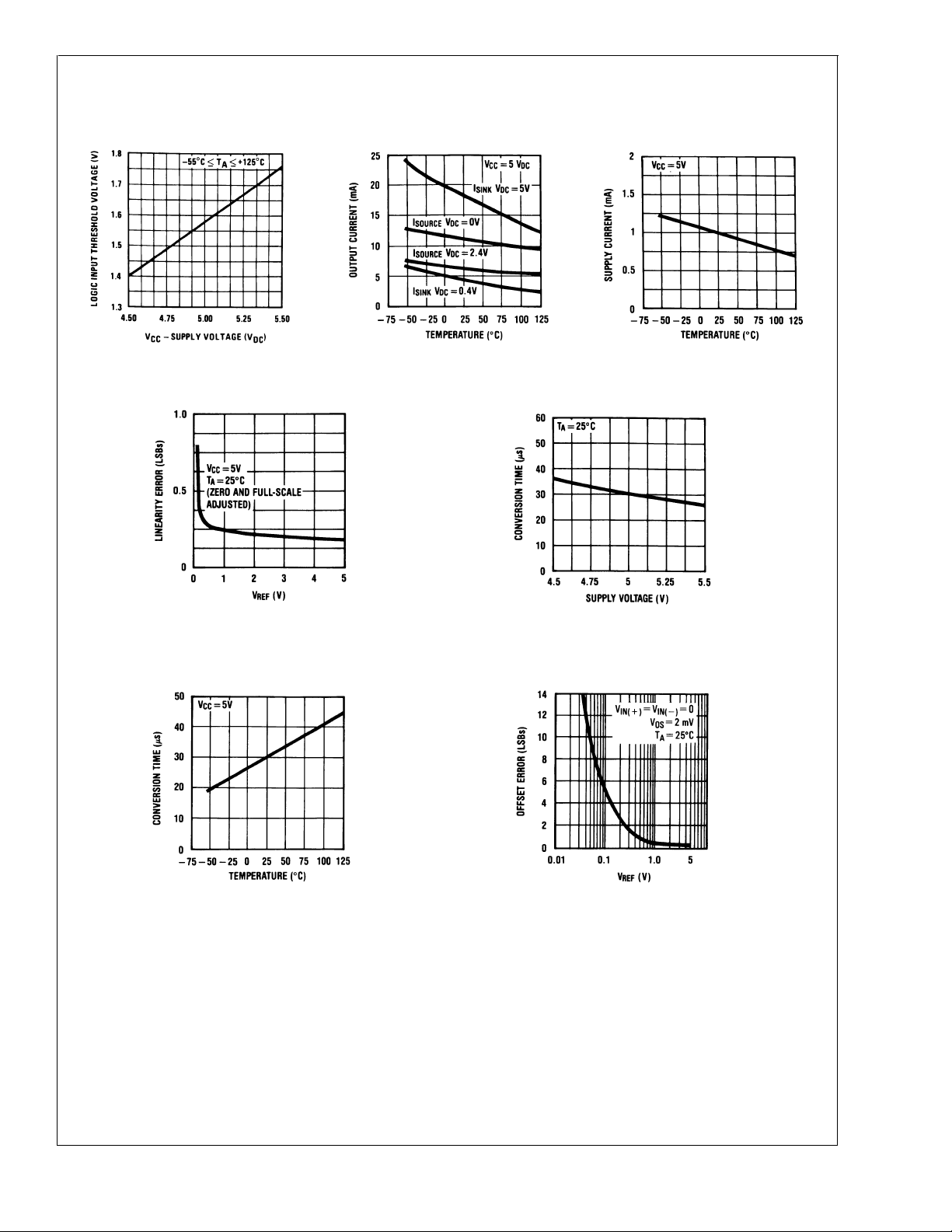
Typical Performance Characteristics
ADC0844/ADC0848
Logic Input Threshold
Voltage vs Supply Voltage
Linearity Error vs V
REF
DS005016-31
Output Current vs
Temperature
DS005016-32
Conversion Time vs V
Power Supply Current vs
Temperature
DS005016-33
SUPPLY
Conversion Time vs
Temperature
DS005016-34
DS005016-36
Unadjusted Offset Error vs
V
Voltage
REF
DS005016-35
DS005016-37
www.national.com5
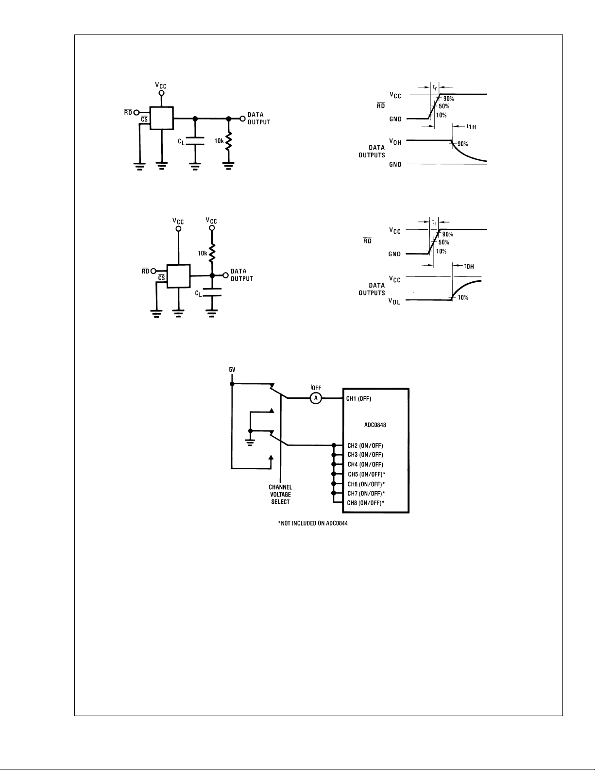
TRI-STATE Test Circuits and Waveforms
t
1H
ADC0844/ADC0848
t
0H
Leakage Current Test Circuit
DS005016-4
DS005016-6
t1H,CL=10pF
DS005016-5
tr=20ns
t0H,CL=10pF
DS005016-7
tr=20ns
www.national.com 6
DS005016-8
 Loading...