

ADC083000
8-Bit, 3 GSPS, High Performance, Low Power A/D
Converter
ADC083000 8-Bit, 3 GSPS, High Performance, Low Power A/D Converter
May 2007
General Description
The ADC083000 is a single, low power, high performance
CMOS analog-to-digital converter that digitizes signals to 8
bits resolution at sampling rates up to 3.4 GSPS. Consuming
a typical 1.9 Watts at 3 GSPS from a single 1.9 Volt supply,
this device is guaranteed to have no missing codes over the
full operating temperature range. The unique folding and interpolating architecture, the fully differential comparator design, the innovative design of the internal sample-and-hold
amplifier and the self-calibration scheme enable a very flat
response of all dynamic parameters up to Nyquist, producing
a high 7.0 Effective Number Of Bits, (ENOB) with a 748 MHz
input signal and a 3 GHz sample rate while providing a 10
Bit Error Rate, (BER). The ADC083000 achieves a 3 GSPS
sampling rate by utilizing both the rising and falling edge of a
1.5 GHz input clock. Output formatting is offset binary and the
LVDS digital outputs are compatible with IEEE 1596.3-1996,
with the exception of an adjustable common mode voltage
between 0.8V and 1.15V.
The ADC has a 1:4 demultiplexer that feeds four LVDS buses
and reduces the output data rate on each bus to a quarter of
the sampling rate.
The converter typically consumes less than 25 mW in the
Power Down Mode and is available in a 128-lead, thermally
enhanced exposed pad LQFP and operates over the Industrial (-40°C ≤ TA ≤ +85°C) temperature range.
-18
Features
Internal Sample-and-Hold
■
Single +1.9V ±0.1V Operation
■
Choice of SDR or DDR output clocking
■
Guaranteed No Missing Codes
■
Serial Interface for Extended Control
■
Adjustment of Input Full-Scale Range and Offset
■
Duty Cycle Corrected Sample Clock
■
Test pattern
■
Key Specifications
Resolution 8 Bits
■
Max Conversion Rate 3 GSPS (min)
■
Bit Error Rate (BER) 10
■
ENOB @ 748 MHz Input 7.0 Bits (typ)
■
SNR @ 748 MHz 44.5 dB (typ)
■
Full Power Bandwidth 3 GHz (typ)
■
Power Consumption
■
Operating 1.9 W (typ)
—
Power Down Mode 25 mW (typ)
—
Applications
Direct RF Down Conversion
■
Digital Oscilloscopes
■
Satellite Set-top boxes
■
Communications Systems
■
Test Instrumentation
■
-18
(typ)
Ordering Information
Industrial Temperature Range
(-40°C < TA < +85°C)
ADC083000CIYB 128-Pin Exposed Pad LQFP
ADC08x3000EB Development Board
© 2007 National Semiconductor Corporation 201932 www.national.com
NS Package
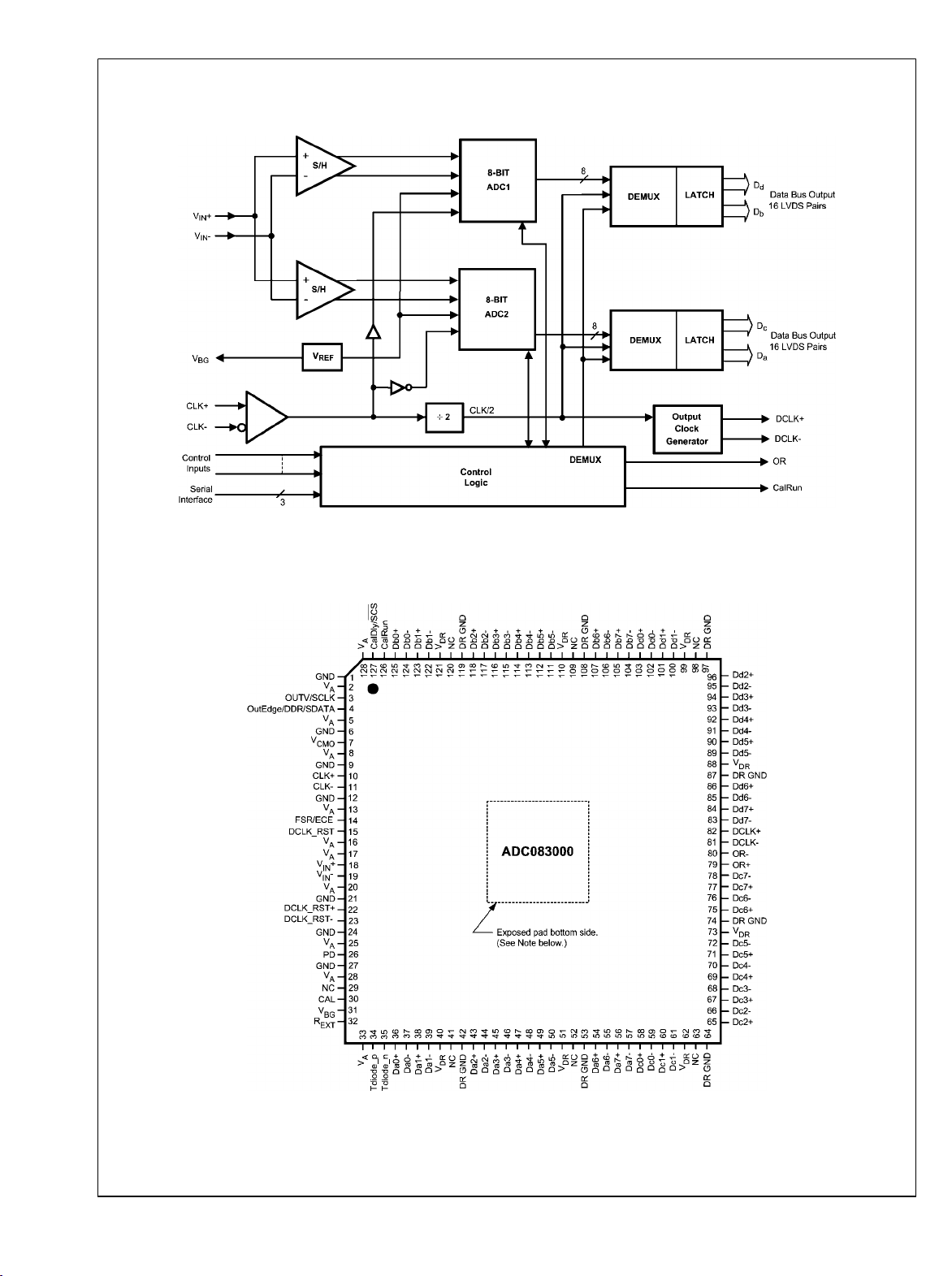
Block Diagram
ADC083000
Pin Configuration
20193253
20193201
Note: The exposed pad on the bottom of the package must be soldered to a ground plane to ensure rated performance.
www.national.com 2

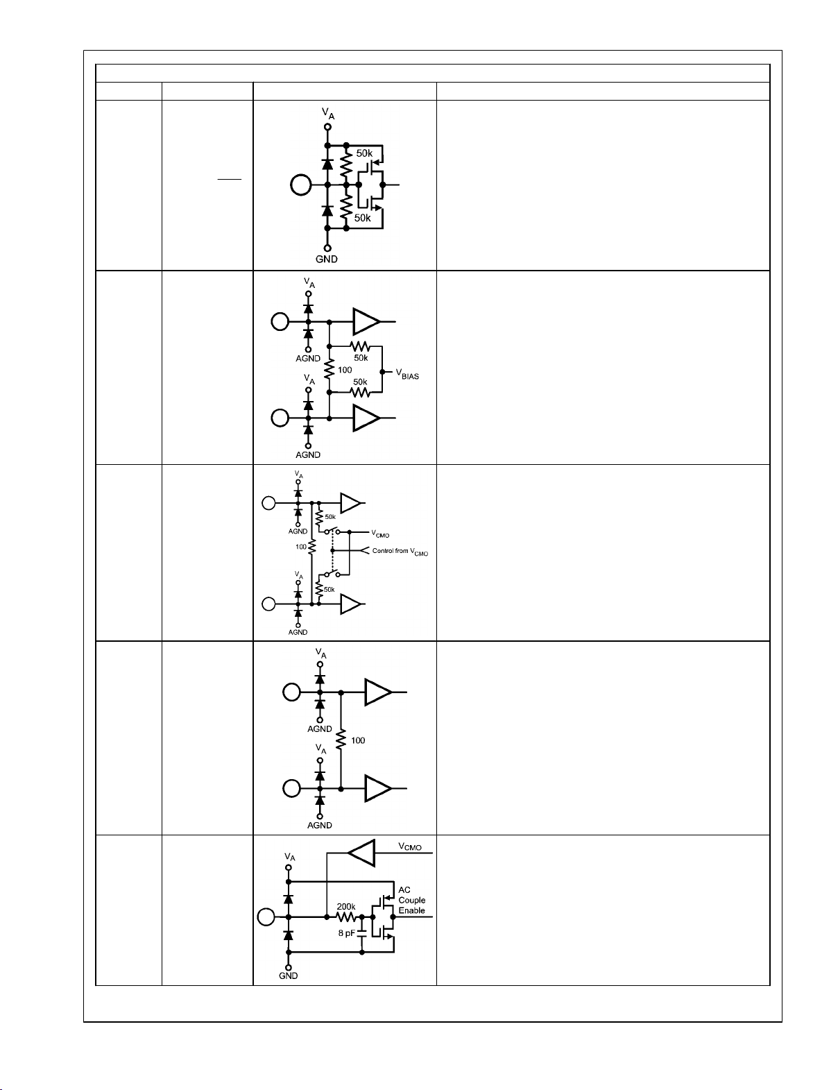
Pin Descriptions and Equivalent Circuits
Pin Functions
Pin No. Symbol Equivalent Circuit Description
Output Voltage Amplitude / Serial Interface Clock
(Input):LVCMOS Tie this pin high for normal differential DCLK
and data amplitude. Ground this pin for a reduced differential
3 OutV / SCLK
OutEdge / DDR /
4
SDATA
output amplitude and reduced power consumption. See Section
1.1.6. When the extended control mode is enabled, this pin
functions as the SCLK input which clocks in the serial data. See
Section 1.2 for details on the extended control mode. See
Section 1.3 for description of the serial interface.
Edge Select / Double Data Rate / Serial Data
(Input):LVCMOS This input sets the output edge of DCLK+ at
which the output data transitions. (See Section 1.1.5.2). When
this pin is floating or connected to 1/2 the supply voltage, DDR
clocking is enabled. When the extended control mode is enabled,
this pin functions as the SDATA input. See Section 1.2 for details
on the extended control mode. See Section 1.3 for description of
the serial interface.
ADC083000
15 DCLK_RST
26 PD
30 CAL
14 FSR/ECE
DCLK Reset
(Input):LVCMOS A positive pulse on this pin is used to reset
and synchronize the DCLK outs of multiple converters. See
Section 1.5 for detailed description. When bit 14 in the
Configuration Register (address 1h) is set to 0b, this singleended DCLK_RST pin is selected.
Power Down
(Input):LVCMOS A logic high on the PD pin puts the entire
device into the Power Down Mode.
Calibration Cycle Initiate
(Input):LVCMOS A minimum 80 input clock cycles logic low
followed by a minimum of 80 input clock cycles high on this pin
initiates the calibration sequence. See Section 2.4.2 for an
overview of self-calibration and Section 2.4.2.2 for a description
of on-command calibration.
Full Scale Range Select / Extended Control Enable
(Input):LVCMOS In non-extended control mode, a logic low on
this pin sets the full-scale differential input range to 600 mV
A logic high on this pin sets the full-scale differential input range
to 820 mV
mode, whereby the serial interface and control registers are
employed, allow this pin to float or connect it to a voltage equal
to VA/2. See Section 1.2 for information on the extended control
mode.
. See Section 1.1.4. To enable the extended control
P-P
P-P
.
3 www.national.com
Pin Functions
Pin No. Symbol Equivalent Circuit Description
ADC083000
127 CalDly / SCS
10
11
18
19
CLK+
CLK-
VIN+
VIN−
Calibration Delay / Serial Interface Chip Select
(Input):LVCMOS With a logic high or low on pin 14, this pin
functions as Calibration Delay and sets the number of input clock
cycles after power up before calibration begins (See Section
1.1.1). With pin 14 floating, this pin acts as the enable pin for the
serial interface input and the CalDly value becomes "0" (short
delay with no provision for a long power-up calibration delay).
Sampling Clock Input
(Input):LVDS The differential clock signal must be a.c. coupled
to these pins. The input signal is sampled on the rising and falling
edge of CLK. See Section 1.1.2 for a description of acquiring the
input and Section 2.3 for an overview of the clock inputs.
Signal Input
(Input):Analog The differential full-scale input range is 600
mV
when the FSR pin is low, or 820 mV
P-P
when the FSR pin
P-P
is high.
22
23
7
www.national.com 4
DCLK_RST+
DCLK_RST-
V
CMO
Sample Clock Reset
(Input):LVDS A positive pulse on this pin is used to reset and
synchronize the DCLK outs of multiple converters. See Section
1.5 for detailed description. When bit 14 in the Configuration
Register (address 1h) is set to 1b, these differential DCLK_RST
pins are selected.
Common Mode Voltage
(Output):Analog - The voltage output at this pin is required to
be the common mode input voltage at VIN+ and VIN− when d.c.
coupling is used. This pin should be grounded when a.c. coupling
is used at the analog input. This pin is capable of sourcing or
sinking 100μA and can drive a load up to 80 pF. See Section 2.2.
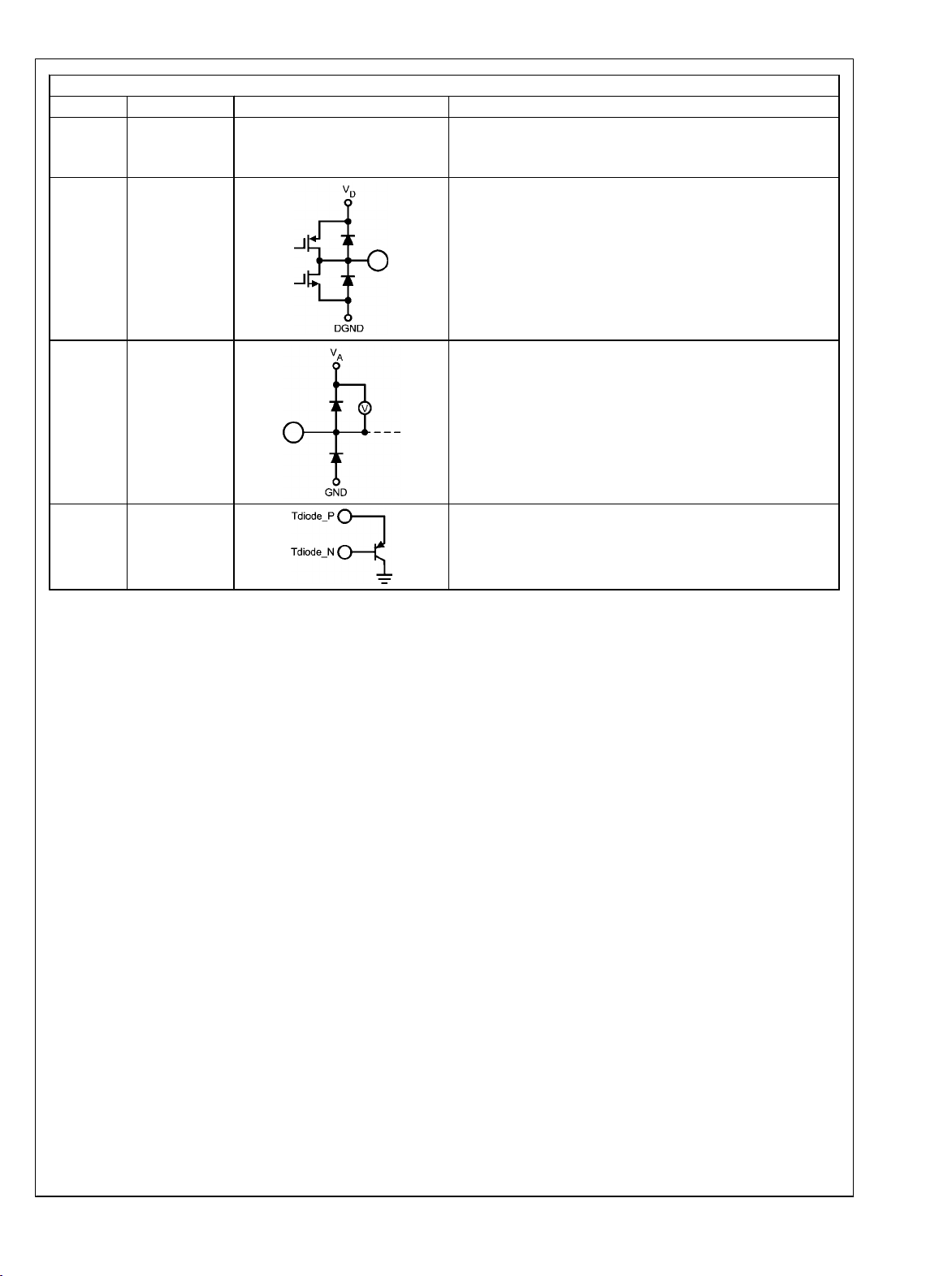
Pin Functions
Pin No. Symbol Equivalent Circuit Description
Bandgap Output Voltage
31
V
BG
(Output):Analog - Capable of 100 μA source/sink and can drive
a load up to 80 pF.
Calibration Running
126 CalRun
(Output):LVCMOS - This pin is at a logic high when calibration
is running.
External Bias Resistor Connection
32
R
EXT
Analog - Nominal value is 3.3k-Ohms (±0.1%) to ground. See
Section 1.1.1.
ADC083000
34
35
Tdiode_P
Tdiode_N
Temperature Diode
Analog - Positive (Anode) and Negative (Cathode) for die
temperature measurements. See Section 2.6.2.
5 www.national.com
Pin Functions
Pin No. Symbol Equivalent Circuit Description
36 / 37
38 / 39
ADC083000
43 / 44
45 / 46
47 / 48
49 / 50
54 / 55
56 / 57
58 / 59
60 / 61
65 / 66
67 / 68
69 / 70
71 / 72
75 / 76
77 / 78
83 / 84
85 / 86
89 / 90
91 / 92
93 / 94
95 / 96
100 / 101
102 / 103
104 / 105
106 / 107
111 / 112
113 / 114
115 / 116
117 / 118
122 / 123
124 / 125
79
80
82
81
Da0+ / Da0Da1+ / Da1-
Da2+ / Da2−
Da3+ / Da3-
Da4+ / Da4−
Da5+ / Da5-
Da6+ / Da6−
Da7+ / Da7-
Dc0+ / Dc0Dc1+ / Dc1-
Dc2+ / Dc2−
Dc3+ / Dc3-
Dc4+ / Dc4−
Dc5+ / Dc5-
Dc6+ / Dc6−
Dc7+ / Dc7-
Dd7− / Dd7+
Dd6- / Dd6+
Dd5− / Dd5+
Dd4- / Dd4+
Dd3- / Dd3+
Dd2- / Dd2+
Dd1− / Dd1+
Dd0- / Dd0+
Db7- / Db7+
Db6- / Db6+
Db5− / Db5+
Db4- / Db4+
Db3− / Db3+
Db2- / Db2+
Db1− / Db1+
Db0- / Db0+
OR+
OR-
DCLK+
DCLK-
A and C Data
(Output):LVDS Data Outputs from the first internal converter.
The data should be extracted in the order ABCD These outputs
should always be terminated with a 100Ω differential resistor.
B and D Data
(Output):LVDS Data Outputs from the second internal
converter. The data should be extracted in the order ABCD
These outputs should always be terminated with a 100Ω
differential resistor.
Out Of Range
(Output):LVDS - A differential high at these pins indicates that
the differential input is out of range (outside the range ±325 mV
or ±435 mV as defined by the FSR pin). These outputs should
always be terminated with a 100Ω differential resistor.
Differential Clock
(Output):LVDS - The Differential Clock outputs are used to latch
the output data. Delayed and non-delayed data outputs are
supplied synchronous to this signal. DCLK is 1/2 the sample
clock rate in SDR mode and 1/4 the sample clock rate in the DDR
mode. These outputs should always be terminated with a 100Ω
differential resistor. The DCLK outputs are not active during the
calibration cycle depending on the setting of Configuration
Register (address 1h), bit- 14 (RTD). DCLK is continuously
present during the calibration cycle when bit-14 is set high (1b)
and is not active during the calibration cycle when set low (0b).
www.national.com 6
Pin Functions
Pin No. Symbol Equivalent Circuit Description
2, 5, 8, 13,
16, 17, 20,
25, 28, 33,
V
A
Analog power supply pins
(Power) - Bypass these pins to ground.
128
40, 51 ,62,
73, 88, 99,
110, 121
1, 6, 9, 12,
21, 24, 27
V
DR
GND
Output Driver power supply pins
(Power) - Bypass these pins to DR GND.
(Gnd) - Ground return for VA.
42, 53, 64,
74, 87, 97,
DR GND
(Gnd) - Ground return for VDR.
108, 119
29,41,52,
63, 98, 109,
NC No Connection Make no connection to these pins
120
ADC083000
7 www.national.com
Absolute Maximum Ratings
(Notes 1, 2)
If Military/Aerospace specified devices are required,
ADC083000
please contact the National Semiconductor Sales Office/
Distributors for availability and specifications.
Supply Voltage (VA, VDR)
Supply Difference
VA - V
DR
Voltage on Any Input Pin −0.15V to (VA + 0.15V)
Ground Difference
|GND - DR GND| 0V to 100 mV
Input Current at Any Pin (Note 3) ±25 mA
Package Input Current (Note 3) ±50 mA
Power Dissipation at TA ≤ 85°C
ESD Susceptibility (Note 4)
Human Body Model
Machine Model
Storage Temperature −65°C to +150°C
0V to -100mV
2.2V
2.3 W
2500V
250V
Operating Ratings (Notes 1, 2)
Ambient Temperature Range
Supply Voltage (VA)
Driver Supply Voltage (VDR) +1.8V to V
Analog Input Common Mode Voltage V
VIN+, VIN- Voltage Range
(Maintaining Common Mode)
Ground Difference
(|GND - DR GND|) 0V
CLK Pins Voltage Range 0V to V
Differential CLK Amplitude 0.4V
−40°C ≤ TA ≤ +85°C
+1.8V to +2.0V
CMO
200mV to V
to 2.0V
P-P
Package Thermal Resistance
Package
128-Lead
Exposed Pad
LQFP
θ
θ
JA
JC (Top of
Package)
26°C / W 10°C / W 2.8°C / W
θ
(Thermal Pad)
Soldering process must comply with National
Semiconductor’s Reflow Temperature Profile specifications.
Refer to www.national.com/packaging. (Note 5)
Converter Electrical Characteristics
The following specifications apply after calibration for VA = VDR = +1.9VDC, OutV = 1.9V, VIN FSR (a.c. coupled) = differential
820mV
Non-Extended Control Mode, SDR Mode, R
limits apply for TA = T
Symbol Parameter Conditions
STATIC CONVERTER CHARACTERISTICS
INL Integral Non-Linearity (Best fit)
DNL Differential Non-Linearity
V
OFF
V
OFF
PFSE Positive Full-Scale Error (Note 9) −1.6 ±25 mV (max)
NFSE
FS_ADJ Full-Scale Adjustment Range Extended Control Mode ±20 ±15 %FS
DYNAMIC CONVERTER CHARACTERISTICS
FPBW Full Power Bandwidth 3 GHz
B.E.R. Bit Error Rate
Gain Flatness
ENOB Effective Number of Bits
SINAD
, CL = 10 pF, Differential, a.c. coupled Sinewave Input Clock, f
P-P
MIN
to T
. All other limits TA = 25°C, unless otherwise noted. (Notes 6, 7)
MAX
= 3300Ω ±0.1%, Analog Signal Source Impedance = 100Ω Differential. Boldface
EXT
DC Coupled, 1MHz Sine Wave Over
Ranged
DC Coupled, 1MHz Sine Wave Over
Ranged
Resolution with No Missing
Codes
8 Bits
Offset Error -0.20 LSB
_ADJ
Input Offset Adjustment Range Extended Control Mode ±45 mV
Negative Full-Scale Error (Note
9)
−1.00 ±25 mV (max)
d.c. to 750 MHz ±0.42 dBFS
d.c. to 1500 MHz ±0.83 dBFS
fIN = 373 MHz, VIN = FSR − 0.5 dB
fIN = 748 MHz, VIN = FSR − 0.5 dB
fIN = 1498 MHz, VIN = FSR − 0.5 dB
Signal-to-Noise Plus Distortion
Ratio
fIN = 373 MHz, VIN = FSR − 0.5 dB
fIN = 748 MHz, VIN = FSR − 0.5 dB
fIN = 1498 MHz, VIN = FSR − 0.5 dB
= 1.5GHz at 0.5V
CLK
with 50% duty cycle, VBG = Floating,
P-P
Typical
(Note 8)
Limits
(Note 8)
±0.35 ±0.9 LSB (max)
±0.20 ±0.6 LSB (max)
-18
10
Error/Sample
7.2 6.85 Bits (min)
7.0 6.6 Bits (min)
6.5 Bits
45 42.2 dB (min)
44.2 40.8 dB (min)
41.1 dB
A
±50mV
A
A
P-P
J-PAD
Units
(Limits)
www.national.com 8
ADC083000
Symbol Parameter Conditions
fIN = 373 MHz, VIN = FSR − 0.5 dB
SNR Signal-to-Noise Ratio
fIN = 748 MHz, VIN = FSR − 0.5 dB
fIN = 1498 MHz, VIN = FSR − 0.5 dB
fIN = 373 MHz, VIN = FSR − 0.5 dB
THD Total Harmonic Distortion
fIN = 748 MHz, VIN = FSR − 0.5 dB
fIN = 1498 MHz, VIN = FSR − 0.5 dB
fIN = 373 MHz, VIN = FSR − 0.5 dB
2nd Harm Second Harmonic Distortion
fIN = 748 MHz, VIN = FSR − 0.5 dB
fIN = 1498 MHz, VIN = FSR − 0.5 dB
fIN = 373 MHz, VIN = FSR − 0.5 dB
3rd Harm Third Harmonic Distortion
fIN = 748 MHz, VIN = FSR − 0.5 dB
fIN = 1498 MHz, VIN = FSR − 0.5 dB
fIN = 373 MHz, VIN = FSR − 0.5 dB
SFDR Spurious-Free dynamic Range
fIN = 748 MHz, VIN = FSR − 0.5 dB
fIN = 1498 MHz, VIN = FSR − 0.5 dB
ANALOG INPUT AND REFERENCE CHARACTERISTICS
FSR pin 14 Low 600
V
IN
Full Scale Analog Differential
Input Range
FSR pin 14 High 820
V
CMI
C
IN
R
IN
Analog Input Common Mode
Voltage
Analog Input Capacitance (Notes
10, 11)
Differential Input Resistance 100
Differential 1.08 pF
Each input pin to ground 2.2 pF
ANALOG OUTPUT CHARACTERISTICS
V
CMO
V
CMO_LVL
TC V
CMO
C
LOAD VCMO
V
BG
TC V
BG
C
LOAD VBG
Common Mode Output Voltage
V
input threshold to set DC
CMO
Coupling mode
Common Mode Output Voltage
Temperature Coefficient
Maximum V
CMO
load
Capacitance
Bandgap Reference Output
Voltage
Bandgap Reference Voltage
Temperature Coefficient
Maximum Bandgap Reference
load Capacitance
I
= ±100 µA
CMO
VA = 1.8V
VA = 2.0V
TA = −40°C to +85°C
80 pF
IBG = ±100 µA
TA = −40°C to +85°C,
IBG = ±100 µA
80 pF
Typical
(Note 8)
Limits
(Note 8)
Units
(Limits)
45.3 43.2 dB (min)
44.5 41.7 dB (min)
41.8 dB
-57 -49 dB (max)
-56 -48 dB (max)
-49.5 dB
−68 dB
−66 dB
−56 dB
−64 dB
−58 dB
−52 dB
57 49 dB (min)
54.5 48 dB (min)
52.0 dB
mV
P-P
mV
P-P
mV
P-P
mV
P-P
mV (min)
mV (max)
Ω (min)
V
CMO
550
650
770
870
V
− 50
CMO
V
+ 50
CMO
95
1.26
105
0.95
1.45
Ω (max)
V (min)
V (max)
0.60 V
0.66 V
118 ppm/°C
1.26
1.20
1.33
V (min)
V (max)
28 ppm/°C
(min)
(max)
(min)
(max)
9 www.national.com

Symbol Parameter Conditions
TEMPERATURE DIODE CHARACTERISTICS
ADC083000
ΔV
BE
Temperature Diode Voltage
192 µA vs. 12 µA,
TJ = 25°C
192 µA vs. 12 µA,
TJ = 85°C
LVDS INPUT CHARACTERISTICS
Sine Wave Clock 0.6
V
ID
Differential Clock Input Level
Square Wave Clock 0.6
I
I
C
IN
Input Current
Input Capacitance (Notes 10, 11)
VIN = 0 or VIN = V
Differential 0.02 pF
Each input to ground 1.5 pF
LVDS OUTPUT CHARACTERISTICS
Measured differentially, OutV = VA, V
V
OD
LVDS Differential Output Voltage
= Floating (Note 15)
Measured differentially, OutV = GND,
VBG = Floating (Note 15)
Δ V
V
V
Δ V
I
OS
Z
O
OS
OS
O DIFF
OS
Change in LVDS Output Swing
Between Logic Levels
Output Offset Voltage,
see Figure 1
Output Offset Voltage,
see Figure 1
Output Offset Voltage Change
Between Logic Levels
Output Short Circuit Current Output+ & Output- connected to 0.8V ±4 mA
Differential Output Impedance 100 Ohms
±1 mV
VBG = Floating
VBG = VA (Note 15)
±1 mV
LVCMOS INPUT CHARACTERISTICS
V
IH
V
IL
C
IN
Logic High Input Voltage (Note 12)
Logic Low Input Voltage (Note 12)
Input Capacitance (Notes 11, 13) Each input to ground 1.2 pF
LVCMOS OUTPUT CHARACTERISTICS
V
OH
V
OL
CMOS H level output
CMOS L level output
IOH = -400uA (Note 12)
IOH = 400uA (Note 12)
POWER SUPPLY CHARACTERISTICS
I
A
I
DR
P
D
Analog Supply Current PD = Low 734 810 mA (max)
Output Driver Supply Current PD = Low 300 410 mA (max)
Power Consumption
PD = Low 1.9 2.3 W (max)
PD = High 25 mW
Typical
(Note 8)
Limits
(Note 8)
Units
(Limits)
71.23 mV
85.54 mV
V
V
V
mV
mV
mV
mV
V
P-P
P-P
P-P
P-P
P-P
P-P
P-P
P-P
(min)
(max)
(min)
(max)
(min)
(max)
(min)
(max)
0.4
2.0
0.4
2.0
A
BG
±1 µA
680
520
470
920
380
720
800 mV
1150 mV
0.85 x V
0.15 x V
A
A
V (min)
V (max)
1.65 1.5 V
0.15 0.3 V
www.national.com 10

ADC083000
Symbol Parameter Conditions
Typical
(Note 8)
Limits
(Note 8)
Units
(Limits)
AC ELECTRICAL CHARACTERISTICS - Sampling Clock
f
CLK1
f
CLK2
t
CYC
t
LC
t
HC
DCLK Duty Cycle (Note 11) 50
t
AD
t
AJ
t
OD
Maximum Input Clock Frequency Sampling rate is 2x clock input 1.7 1.5 GHz (min)
Minimum Input Clock Frequency Sampling rate is 2x clock input 500 MHz
Input Clock Duty Cycle
500MHz ≤ Input clock frequency ≤ 1.5
GHz (Note 12)
50
20
80
% (min)
% (max)
Input Clock Low Time (Note 11) 333 133 ps (min)
Input Clock High Time (Note 11) 333 133 ps (min)
Sampling (Aperture) Delay
Input CLK transition to Acquisition of
Data
45
55
1.4 ns
% (min)
% (max)
Aperture Jitter 0.55 ps rms
Input Clock to Data Output Delay
(in addition to Pipeline Delay)
50% of Input Clock transition to 50% of
Data transition
3.7 ns
Dd Outputs 13
Pipeline Delay (Latency)
(Notes 11, 14)
Db Outputs 14
Dc Outputs 13.5
Input Clock
Cycles
Da Outputs 14.5
AC ELECTRICAL CHARACTERISTICS - Output Clock and Data (Note 16)
t
t
LHT
HLT
LH Transition Time - Differential 10% to 90% 150 ps
HL Transition Time - Differential 10% to 90% 150 ps
50% of DCLK transition to 50% of Data
t
SKEWO
DCLK to Data Output Skew
transition, SDR Mode
±50 ps (max)
and DDR Mode, 0° DCLK (Note 11)
t
OSU
t
OH
Data to DCLK Set-Up Time DDR Mode, 90° DCLK (Note 12) 570 ps
DCLK to Data Hold Time DDR Mode, 90° DCLK (Note 12) 555 ps
AC ELECTRICAL CHARACTERISTICS - Serial Interface Clock
f
SCLK
t
SS
t
HS
Serial Clock Frequency (Note 11) 67 MHz
Data to Serial Clock Setup Time (Note 11) 2.5 ns (min)
Data to Serial Clock Hold Time (Note 11) 1 ns (min)
Serial Clock Low Time 6 ns (min)
Serial Clock High Time 6 ns (min)
AC ELECTRICAL CHARACTERISTICS - General Signals
t
SR
t
HR
t
PWR
t
WU
t
CAL
t
CAL_L
t
CAL_H
t
CalDly
t
CalDly
Setup Time DCLK_RST±
Hold Time DCLK_RST± 30 ps
(Note 12)
90 ps
Pulse Width DCLK_RST± (Note 11) 4 CLK± Cyc. (min)
PD low to Rated Accuracy
Conversion (Wake-Up Time)
Calibration Cycle Time
(Note 11) 1 µs
5
1.4 x 10
CLK± Cyc.
CAL Pin Low Time See Figure 8 (Note 11) 80 CLK± Cyc. (min)
CAL Pin High Time See Figure 8 (Note 11) 80 CLK± Cyc.(min)
Calibration delay determined by
pin 127
Calibration delay determined by
pin 127
See Section 1.1.1, Figure 8, (Note 11)
See Section 1.1.1, Figure 8, (Note 11)
25
2
2
31
CLK± Cyc.(min)
CLK± Cyc.(max)
11 www.national.com
Note 1: Absolute Maximum Ratings indicate limits beyond which damage to the device may occur. There is no guarantee of operation at the Absolute Maximum
Ratings. Operating Ratings indicate conditions for which the device is functional, but do not guarantee specific performance limits. For guaranteed specifications
and test conditions, see the Electrical Characteristics. The guaranteed specifications apply only for the test conditions listed. Some performance characteristics
may degrade when the device is not operated under the listed test conditions.
Note 2: All voltages are measured with respect to GND = DR GND = 0V, unless otherwise specified.
ADC083000
Note 3: When the input voltage at any pin exceeds the power supply limits (that is, less than GND or greater than VA), the current at that pin should be limited to
25 mA. The 50 mA maximum package input current rating limits the number of pins that can safely exceed the power supplies with an input current of 25 mA to
two. This limit is not placed upon the power, ground and digital output pins.
Note 4: Human body model is 100 pF capacitor discharged through a 1.5 kΩ resistor. Machine model is 220 pF discharged through ZERO Ohms.
Note 5: Reflow temperature profiles are different for lead-free and non-lead-free packages.
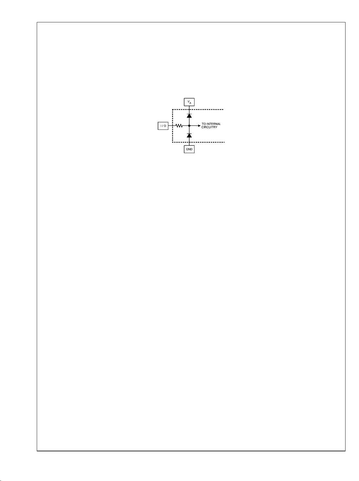
Note 6: The analog inputs are protected as shown below. Input voltage magnitudes beyond the Absolute Maximum Ratings may damage this device.
20193204
Note 7: To guarantee accuracy, it is required that VA and VDR be well bypassed. Each supply pin must be decoupled with separate bypass capacitors. Additionally,
achieving rated performance requires that the backside exposed pad be well grounded.
Note 8: Typical figures are at TA = 25°C, and represent most likely parametric norms. Test limits are guaranteed to National's AOQL (Average Outgoing Quality
Level).
Note 9: Calculation of Full-Scale Error for this device assumes that the actual reference voltage is exactly its nominal value. Full-Scale Error for this device,
therefore, is a combination of Full-Scale Error and Reference Voltage Error. See Figure 2. For relationship between Gain Error and Full-Scale Error, see
Specification Definitions for Gain Error.
Note 10: The analog and clock input capacitances are die capacitances only. Additional package capacitances of 0.65 pF differential and 0.95 pF each pin to
ground are isolated from the die capacitances by lead and bond wire inductances.
Note 11: This parameter is guaranteed by design and is not tested in production.
Note 12: This parameter is guaranteed by design and/or characterization and is not tested in production.
Note 13: The digital control pin capacitances are die capacitances only. Additional package capacitance of 1.6 pF each pin to ground are isolated from the die
capacitances by lead and bond wire inductances.
Note 14: Each of the two converters of the ADC083000 has two LVDS output buses, which each clock data out at one quarter the sample rate. Bus Db has a
pipeline latency that is one Input Clock cycle less than the latency of bus Dd. Likewise, bus Da has a pipeline latency that is one Input Clock cycle less than the
latency of bus Dc.
Note 15: Tying VBG to the supply rail will increase the output offset voltage (VOS) by 400mv (typical), as shown in the VOS specification above. Tying VBG to the
supply rail will also affect the differential LVDS output voltage (VOD), causing it to increase by 40mV (typical).
Note 16: All parameters are measured through a transmission line and 100Ω termination using a 0.33pF load oscilloscope probe.
Specification Definitions
APERTURE (SAMPLING) DELAY is the amount of delay,
measured from the sampling edge of the Clock input, after
which the signal present at the input pin is sampled inside the
device.
APERTURE JITTER (tAJ) is the variation in aperture delay
from sample to sample. Aperture jitter shows up as input
noise.
Bit Error Rate (B.E.R.) is the probability of error and is defined as the probable number of errors per unit of time divided
by the number of bits seen in that amount of time. A B.E.R. of
-18
10
corresponds to a statistical error in one bit about every
four (4) years.
CLOCK DUTY CYCLE is the ratio of the time that the clock
wave form is at a logic high to the total time of one clock period.
DIFFERENTIAL NON-LINEARITY (DNL) is the measure of
the maximum deviation from the ideal step size of 1 LSB.
Measured at 3 GSPS with a ramp input.
EFFECTIVE NUMBER OF BITS (ENOB, or EFFECTIVE
BITS) is another method of specifying Signal-to-Noise and
Distortion Ratio, or SINAD. ENOB is defined as (SINAD −
1.76) / 6.02 and says that the converter is equivalent to a per-
FULL POWER BANDWIDTH (FPBW) is a measure of the
frequency at which the reconstructed output fundamental
drops 3 dB below its low frequency value for a full scale input.
GAIN ERROR is the deviation from the ideal slope of the
transfer function. It can be calculated from Offset and FullScale Errors:
Positive Gain Error = Offset Error − Positive Full-Scale
Error
Negative Gain Error = −(Offset Error − Negative FullScale Error)
Gain Error = Negative Full-Scale Error − Positive FullScale Error = Positive Gain Error + Negative Gain Error
INTEGRAL NON-LINEARITY (INL) is a measure of the deviation of each individual code from a straight line through the
input to output transfer function. The deviation of any given
code from this straight line is measured from the center of that
code value. The best fit method is used.
INTERMODULATION DISTORTION (IMD) is the creation of
additional spectral components as a result of two sinusoidal
frequencies being applied to the ADC input at the same time.
It is defined as the ratio of the power in the second and third
order intermodulation products to the power in one of the
original frequencies. IMD is usually expressed in dBFS.
fect ADC of this (ENOB) number of bits.
www.national.com 12

ADC083000
LSB (LEAST SIGNIFICANT BIT) is the bit that has the small-
est value or weight of all bits. This value is
n
VFS / 2
where VFS is the differential full-scale amplitude of VIN as set
by the FSR input (pin-14) and "n" is the ADC resolution in bits,
which is 8 for the ADC083000.
LVDS DIFFERENTIAL OUTPUT VOLTAGE (VOD) is the absolute value of the difference between the VD+ & VD- outputs;
each measured with respect to Ground.
20193246
FIGURE 1.
LVDS OUTPUT OFFSET VOLTAGE (VOS) is the midpoint
between the D+ and D- pins output voltage; ie., [(VD+) +
( VD-)]/2.
MISSING CODES are those output codes that are skipped
and will never appear at the ADC outputs. These codes cannot be reached with any input value.
MSB (MOST SIGNIFICANT BIT) is the bit that has the largest
value or weight. Its value is one half of full scale.
NEGATIVE FULL-SCALE ERROR (NFSE) is a measure of
how far the last code transition is from the ideal 1/2 LSB above
a differential -VIN / 2. For the ADC083000 the reference voltage is assumed to be ideal, so this error is a combination of
full-scale error and reference voltage error.
OFFSET ERROR (V
scale point is from the ideal zero voltage differential input.
) is a measure of how far the mid-
OFF
Offset Error = Actual Input causing average of 8k samples to result in an average code of 127.5.
OUTPUT DELAY (tOD) is the time delay from 50% point of the
input clock transition, CLK, to the 50% point of the updated
data transition at the output pins.
OVER-RANGE RECOVERY TIME is the time required after
the differential input voltages goes from ±1.2V to 0V for the
converter to recover and make a conversion with its rated accuracy.
PIPELINE DELAY (LATENCY) is the number of input clock
cycles between initiation of conversion and when that data is
presented to the output driver stage. New data is available at
every clock cycle, but the data lags the conversion by the
Pipeline Delay plus the tOD.
POSITIVE FULL-SCALE ERROR (PFSE) is a measure of
how far the last code transition is from the ideal 1-1/2 LSB
below a differential +VIN / 2. For the ADC083000 the reference
voltage is assumed to be ideal, so this error is a combination
of full-scale error and reference voltage error.
POWER SUPPLY REJECTION RATIO (PSRR) can be one
of two specifications. PSRR1 (DC PSRR) is the ratio of the
change in full-scale error that results from a power supply
voltage change from 1.8V to 2.0V. PSRR2 (AC PSRR) is a
measure of how well an a.c. signal riding upon the power
supply is rejected from the output and is measured with a 248
MHz, 50 mV
ratio of the output amplitude of that signal at the output to its
signal riding upon the power supply. It is the
P-P
amplitude on the power supply pin. PSRR is expressed in dB.
SIGNAL TO NOISE RATIO (SNR) is the ratio, expressed in
dB, of the rms value of the input signal at the output to the rms
value of the sum of all other spectral components below onehalf the sampling frequency, not including harmonics or d.c.
SIGNAL TO NOISE PLUS DISTORTION (S/(N+D) or
SINAD) is the ratio, expressed in dB, of the rms value of the
input signal at the output to the rms value of all of the other
spectral components below half the input clock frequency, including harmonics but excluding d.c.
SPURIOUS-FREE DYNAMIC RANGE (SFDR) is the difference, expressed in dB, between the rms values of the input
signal at the output and the peak spurious signal, where a
spurious signal is any signal present in the output spectrum
that is not present at the input, excluding d.c.
TOTAL HARMONIC DISTORTION (THD) is the ratio expressed in dB, of the rms total of the first nine harmonic levels
at the output to the level of the fundamental at the output. THD
is calculated as
where Af1 is the RMS power of the fundamental (output) frequency and Af2 through A
harmonic frequencies in the output spectrum.
are the RMS power of the first 9
f10
– Second Harmonic Distortion (2nd Harm) is the difference, expressed in dB, between the RMS power in the input
frequency seen at the output and the power in its 2nd harmonic level at the output.
– Third Harmonic Distortion (3rd Harm) is the difference
expressed in dB between the RMS power in the input frequency seen at the output and the power in its 3rd harmonic
level at the output.
13 www.national.com

Transfer Characteristic
ADC083000
FIGURE 2. Input / Output Transfer Characteristic
20193222
www.national.com 14

Timing Diagrams
ADC083000
20193214
FIGURE 3. ADC083000 Timing — SDR Clocking
FIGURE 4. ADC083000 Timing — DDR Clocking
15 www.national.com
20193259

ADC083000
20193220
FIGURE 5. Clock Reset Timing in DDR Mode
FIGURE 6. Clock Reset Timing in SDR Mode with OUTEDGE Low
FIGURE 7. Clock Reset Timing in SDR Mode with OUTEDGE High
20193223
20193224
www.national.com 16

FIGURE 8. Calibration and On-Command Calibration Timing
ADC083000
20193225
FIGURE 9. Serial Interface Timing
20193219
17 www.national.com

Typical Performance Characteristics V
A=VDR
=1.9V, F
=1500MHz, TA=25°C unless otherwise stated.
CLK
ADC083000
DNL vs. TEMPERATURE
ENOB vs. TEMPERATURE
20193268
POWER DISSIPATION vs. SAMPLE RATE
20193269
ENOB vs. SUPPLY VOLTAGE
20193270
ENOB vs. SAMPLE RATE
20193272
www.national.com 18
20193271
ENOB vs. INPUT FREQUENCY
20193273

ADC083000
SNR vs. TEMPERATURE
SNR vs. SAMPLE RATE
20193274
SNR vs. SUPPLY VOLTAGE
20193275
SNR vs. INPUT FREQUENCY
THD vs. TEMPERATURE
20193276
20193278
20193277
THD vs. SUPPLY VOLTAGE
20193279
19 www.national.com

ADC083000
THD vs. SAMPLE RATE
THD vs. INPUT FREQUENCY
SFDR vs. TEMPERATURE
SFDR vs. SAMPLE RATE
20193280
20193282
20193281
SFDR vs. SUPPLY VOLTAGE
20193283
SFDR vs. INPUT FREQUENCY
20193284
www.national.com 20
20193285

ADC083000
Spectral Response at FIN = 748 MHZ
FULL POWER BANDWIDTH
20193287
Spectral Response at FIN = 1497 MHZ
20193288
20193290
21 www.national.com

1.0 Functional Description
The ADC083000 is a versatile A/D Converter with an innovative architecture permitting very high speed operation. The
controls available ease the application of the device to circuit
ADC083000
solutions. Optimum performance requires adherence to the
provisions discussed here and in the Applications Information
Section.
While it is generally poor practice to allow an active pin to float,
pins 4 and 14 of the ADC083000 are designed to be left floating without jeopardy. In all discussions throughout this data
sheet, whenever a function is called by allowing a control pin
to float, connecting that pin to a potential of one half the V
supply voltage will have the same effect as allowing it to float.
1.1 OVERVIEW
The ADC083000 uses a calibrated folding and interpolating
architecture that achieves over 7.2 effective bits. The use of
folding amplifiers greatly reduces the number of comparators
and power consumption. Interpolation reduces the number of
front-end amplifiers required, minimizing the load on the input
signal and further reducing power requirements. In addition
to other things, on-chip calibration reduces the INL bow often
seen with folding architectures. The result is an extremely
fast, high performance, low power converter.
The analog input signal that is within the converter's input
voltage range is digitized to eight bits at speeds of 1.0 GSPS
to 3.0 GSPS, typical. Differential input voltages below negative full-scale will cause the output word to consist of all
zeroes. Differential input voltages above positive full-scale
will cause the output word to consist of all ones. Either of
these conditions at the analog input will cause the OR (Out of
Range) output to be activated. This single OR output indicates
when the output code from the converter is below negative
full scale or above positive full scale.
The ADC083000 demultiplexes the data at 1:4 and is output
on all four output busses at a quarter of the ADC sampling
rate. The outputs must be interleaved by the user to provide
output words at the full conversion rate.
The output levels may be selected to be normal or reduced
voltage. Using reduced levels saves power but could result in
erroneous data capture of some or all of the bits, especially
at higher sample rates and in marginally designed systems.
1.1.1 Calibration
A calibration is performed upon power-up and can also be
invoked by the user upon command. Calibration trims the
100Ω analog input differential termination resistor and minimizes full-scale error, offset error, DNL and INL, resulting in
maximizing SNR, THD, SINAD (SNDR) and ENOB. Internal
bias currents are also set with the calibration process. All of
this is true whether the calibration is performed upon power
up or is performed upon command. Running the calibration is
an important part of this chip's functionality and is required in
order to obtain adequate performance. In addition to the requirement to be run at power-up, calibration must be re-run
by the user whenever the state of the FSR pin is changed. For
best performance, we recommend an on command calibration be run after initial power up and the device has reached
a stable temperature. Also, we recommend that an on command calibration be run whenever the operating temperature
changes significantly relative to the specific system performance requirements. See Section 2.4.2.2 for more information. Calibration can not be initiated or run while the device is
in the power-down mode. See Section 1.1.7 for information
on the interaction between Power Down and Calibration.
In normal operation, calibration is performed just after application of power and whenever a valid calibration command is
given, which is holding the CAL pin low for at least 80 input
clock cycles, then hold it high for at least another 80 input
clock cycles. The time taken by the calibration procedure is
specified in the A.C. Characteristics Table. Holding the CAL
pin high upon power up will prevent the calibration process
from running until the CAL pin experiences the above-mentioned 80 input clock cycles low followed by 80 cycles high.
CalDly (pin 127) is used to select one of two delay times after
the application of power to the start of calibration. This calibration delay is 225 input clock cycles (about 22 ms at 3
A
GSPS) with CalDly low, or 231 input clock cycles (about 1.4
seconds at 3 GSPS) with CalDly high. These delay values
allow the power supply to come up and stabilize before calibration takes place. If the PD pin is high upon power-up, the
calibration delay counter will be disabled until the PD pin is
brought low. Therefore, holding the PD pin high during power
up will further delay the start of the power-up calibration cycle.
The best setting of the CalDly pin depends upon the poweron settling time of the power supply.
Calibration Operation Notes:
•
During the calibration cycle, the OR output may be active
as a result of the calibration algorithm. All data on the
output pins and the OR output are invalid during the
calibration cycle.
•
During the power-up calibration and during the oncommand calibration when Resistor Trim Disable
(address: 1h, bit 13) is not active (0b) , all clocks are halted
on chip, including internal clocks and DCLK, while the
input termination resistor is trimmed to a value that is equal
to R
/ 33. This is to reduce noise during the input
EXT
resistor calibration portion of the calibration cycle. See
Section 2.4.2.2 for information on maintaining DCLK
operation during on-command calibration.
This external resistor is located between pin 32 and
ground. R
input termination resistor is trimmed to be 100 Ω. Because
R
is also used to set the proper current for the Track
EXT
and Hold amplifier, for the preamplifiers and for the
comparators, other values of R
•
The CalRun output is high whenever the calibration
must be 3300 Ω ±0.1%. With this value, the
EXT
should not be used.
EXT
procedure is running. This is true whether the calibration
is done at power-up or on-command.
1.1.2 Acquiring the Input
Data is acquired at the rising and falling edge of CLK+ (pin
10) and the digital equivalent of that data is available at the
digital outputs 13 input clock cycles later for the Dd output
bus, 13.5 input clock cycles later for Dc output bus, 14 input
clock cycles later for the Db output bus and 14.5 input clock
cycles later for the Da output bus. See Table 1. There is an
additional internal delay called tOD before the data is available
at the outputs. See Figure 3 and Figure 4. The ADC083000
will convert as long as the input clock signal is present. The
fully differential comparator design and the innovative design
of the sample-and-hold amplifier, together with calibration,
enables a very flat SINAD/ENOB response beyond 1.5 GHz.
The ADC083000 output data signaling is LVDS and the output
format is offset binary.
1.1.3 Control Modes
Much of the user control can be accomplished with several
control pins that are provided. Examples include initiation of
the calibration cycle, power down mode and full scale range
setting. However, the ADC083000 also provides an Extended
www.national.com 22

ADC083000
Control mode whereby a serial interface is used to access
register-based control of several advanced features. The Extended Control mode is not intended to be enabled and
disabled dynamically. Rather, the user is expected to employ
either the normal control mode or the Extended Control mode
at all times. When the device is in the Extended Control mode,
pin-based control of several features is replaced with registerbased control and those pin-based controls are disabled.
These pins are OutV (pin 3), OutEdge/DDR (pin 4), FSR (pin
14). See Section 1.2 for details on the Extended Control
mode.
1.1.4 The Analog Inputs
The ADC083000 must be driven with a differential input signal. Operation with a single-ended signal is not recommended. It is important that the input signals are either a.c. coupled
to the inputs with the V
the V
equal to the V
is used.
pin left floating. An input common mode voltage
CMO
output must be provided when d.c. coupling
CMO
pin grounded, or d.c. coupled with
CMO
Two full-scale range settings are provided with pin 14 (FSR).
A high on pin 14 causes an input full-scale range setting of
820 mV
range setting of 600 mV
, while grounding pin 14 causes an input full-scale
P-P
P-P
.
In the Extended Control mode, the full-scale input range can
be set to values between 560 mV
a serial interface. See Section 2.2
and 840 mV
P-P
through
P-P
1.1.5 Clocking
The ADC083000 sampling clock (CLK+/CLK-) must be driven
with an a.c. coupled, differential clock signal. Section 2.3 de-
scribes the use of the clock input pins. A differential LVDS
output clock (DCLK) is available for use in latching the ADC
output data into whatever device is used to receive the data.
The ADC083000 offers options for CLK+/CLK- and DCLK
clocking. For DCLK, the clock edge on which output data
transitions, and a choice of Single Data Rate (SDR) or Double
Data Rate (DDR) outputs are available.
The sampling clock CLK has optional duty cycle correction as
part of its circuit. This feature is enabled by default and provides improved ADC clocking. This circuitry allows the ADC
to be clocked with a signal source having a duty cycle ratio of
80 / 20 % (worst case).
1.1.5.1 Output Demultiplexer
The ADC083000 utilizes both the rising and falling edge of the
input clock resulting in the overall sample rate being twice the
input clock frequency, or 3GSPS with a 1.5 GHz input clock.
The demultiplexer outputs data on each of the four output
busses at 750MHz with a 1.5GHz input clock.
All data is available in parallel at the output. The four bytes of
parallel data that are output with each clock is in the following
sampling order, from the earliest to the latest: Da, Db, Dc, Dd.
Table 1 indicates what the outputs represent for the various
sampling possibilities.
The ADC083000 includes an automatic clock phase background calibration feature which automatically and continuously adjusts the phase of the ADC input clock. This feature
removes the need to manually adjust the clock phase and
provides optimal ENOB performance.
TABLE 1. Input Channel Samples Produced at Data Outputs
Data Outputs* Input/Output Relationship
Dd ADC1 sampled with the fall of CLK, 13 cycles earlier
Db ADC1 sampled with the fall of CLK, 14 cycles earlier
Dc ADC2 sampled with the rise of CLK, 13.5 cycles earlier
Da ADC2 sampled with the rise of CLK, 14.5 cycles earlier
* Always sourced with respect to fall of DCLK
1.1.5.2 OutEdge Setting
To help ease data capture in the SDR mode, the output data
may be caused to transition on either the positive or the negative edge of the output data clock (DCLK). This is chosen
with the OutEdge input (pin 4). A high on the OutEdge input
pin causes the output data to transition on the rising edge of
DCLK, while grounding this input causes the output to transition on the falling edge of DCLK. See Section 2.4.3.
1.1.5.3 Double Data Rate
A choice of single data rate (SDR) or double data rate (DDR)
output is offered. When the device is in DDR mode, address
1h, bit-8 must be set to 0b. With single data rate the output
clock (DCLK) frequency is the same as the data rate of the
two output buses. With double data rate the DCLK frequency
is half the data rate and data is sent to the outputs on both
edges of DCLK. DDR clocking is enabled in non-Extended
Control mode by allowing pin 4 to float.
1.1.6 The LVDS Outputs
The data outputs, the Out Of Range (OR) and DCLK, are
LVDS. Output current sources provide 3 mA of output current
to a differential 100 Ohm load when the OutV input (pin 3) is
high or 2.2 mA when the OutV input is low. For short LVDS
lines and low noise systems, satisfactory performance may
be realized with the OutV input low, which results in lower
power consumption. If the LVDS lines are long and/or the
system in which the ADC083000 is used is noisy, it may be
necessary to tie the OutV pin high.
The LVDS data outputs have a typical common mode voltage
of 800mV when the VBG pin is unconnected and floating. This
common mode voltage can be increased to 1.150V by tying
the VBG pin to VA if a higher common mode is required.
IMPORTANT NOTE: Tying the VBG pin to VA will also in-
crease the differential LVDS output voltage (VOD) by up to
40mV.
1.1.7 Power Down
The ADC083000 is in the active state when the Power Down
pin (PD) is low. When the PD pin is high, the device is in the
power down mode. In this power down mode the data output
pins (positive and negative) including DCLK+/- and OR +/- are
put into a high impedance state and the devices power consumption is reduced to a minimal level.
If the PD input is brought high while a calibration is running,
the device will not go into power down until the calibration
sequence is complete. However, if power is applied and PD
23 www.national.com

is already high, the device will not begin the calibration sequence until the PD input goes low. If a manual calibration is
requested while the device is powered down, the calibration
will not begin at all. That is, the manual calibration input is
completely ignored in the power down state.
ADC083000
1.2 NORMAL/EXTENDED CONTROL
The ADC083000 may be operated in one of two modes. In
the Normal Mode, the user affects available configuration and
Feature Normal Control Mode Extended Control Mode
SDR or DDR Clocking Selected with pin 4
DDR Clock Phase Not Selectable (0° Phase Only)
SDR Data transitions with rising or falling
DCLK edge
Selected with pin 4
LVDS output level Selected with pin 3
Power-On Calibration Delay Delay Selected with pin 127 Short delay only.
Options (600 mV
Full-Scale Range
selected with pin 14. Selected range
applies to both channels.
Input Offset Adjust Not possible
Sampling Clock Phase Adjustment
The Clock Phase is adjusted
automatically
Test Pattern Not Possible
Resistor Trim Disable Not possible
control of the device through several control pins. The "extended control mode" provides additional configuration and
control options through a serial interface and a set of 6 registers. The two control modes are selected with pin 14 (FSR/
ECE: Extended Control Enable). The choice of control modes
is required to be a fixed selection and is not intended to be
switched dynamically while the device is operational.
Table 2 shows how several of the device features are affected
by the control mode chosen.
TABLE 2. Features and Modes
or 820 mV
P-P
P-P
)
Selected with nDE in the Configuration
Register (1h; bit-10). When the device is
in DDR mode, address 1h, bit-8 must be
set to 0b.
Selected with DCP in the Configuration
Register (1h; bit-11).
Selected with OE in the Configuration
Register (1h; bit-8).
Selected with the OV in the
Configuration Register (1h; bit-9).
Up to 512 step adjustments over a
nominal range of 560 mV to 840 mV in
the Configuration Register (3h; bits-7
thru 15).
Up to ±45 mV adjustments in 512 steps
in the Configuration Register (2h; bits-7
thru 15).
The clock phase can be adjusted
manually through the Fine & Coarse
registers (Dh and Eh).
A test pattern can be made present at the
data outputs by selecting TPO in the
Configuration Register (Fh; bit-11).
The DCLK outputs will continuously be
present when RTD is selected in the
Configuration Register (1h; bit-13)
www.national.com 24

ADC083000
The default state of the Extended Control Mode is set upon
power-on reset (internally performed by the device) and is
shown in Table 3.
TABLE 3. Extended Control Mode Operation (Pin 14
Floating)
Feature
Extended Control Mode
Default State
SDR or DDR Clocking DDR Clocking
DDR Clock Phase
LVDS Output Amplitude
Data changes with DCLK
edge (0° phase)
Normal amplitude
(710 mV
P-P
)
Calibration Delay Short Delay
Full-Scale Range
Input Offset Adjust
700 mV nominal for both
channels
No adjustment for either
channel
Trim enabled, DCLK not
Resistor Trim Disable
continuously present at
output
Test Pattern Not present at output
1.3 THE SERIAL INTERFACE
The 3-pin serial interface is enabled only when the device is
in the Extended Control mode. The pins of this interface are
Serial Clock (SCLK), Serial Data (SDATA) and Serial Interface Chip Select (SCS) Eight write only registers are accessible through this serial interface.
SCS: This signal should be asserted low while accessing a
register through the serial interface. Setup and hold times with
respect to the SCLK must be observed.
SCLK: Serial data input is accepted with the rising edge of
this signal.
SDATA: Each register access requires a specific 32-bit pattern at this input. This pattern consists of a header, register
address and register value. The data is shifted in MSB first.
Setup and hold times with respect to the SCLK must be observed. SeeFigure 9.
Each Register access consists of 32 bits, as shown in Figure
9 of the Timing Diagrams. The fixed header pattern is 0000
0000 0001 (eleven zeros followed by a 1). The loading sequence is such that a "0" is loaded first. These 12 bits form
the header. The next 4 bits are the address of the register that
is to be written to and the last 16 bits are the data written to
the addressed register. The addresses of the various registers are indicated in Table 4.
Refer to the Register Description (Section 1.4) for information
on the data to be written to the registers.
Subsequent register accesses may be performed immediately, starting with the 33rd SCLK. This means that the SCS input
does not have to be de-asserted and asserted again between
register addresses. It is possible, although not recommended,
to keep the SCS input permanently enabled (at a logic low)
when using extended control.
IMPORTANT NOTE: The Serial Interface should not be used
when calibrating the ADC. Doing so will impair the performance of the device until it is re-calibrated correctly. Programming the serial registers will also reduce dynamic
performance of the ADC for the duration of the register access
time.
TABLE 4. Register Addresses
4-Bit Address
Loading Sequence:
A3 loaded after H0, A0 loaded last
A3 A2 A1 A0 Hex Register Addressed
0 0 0 0 0h Reserved
0 0 0 1 1h Configuration
0 0 1 0 2h Offset
0 0 1 1 3h Full-Scale Voltage
Adjust
0 1 0 0 4h Reserved
0 1 0 1 5h Reserved
0 1 1 0 6h Reserved
0 1 1 1 7h Reserved
1 0 0 0 8h Reserved
1 0 0 1 9h Reserved
1 0 1 0 Ah Reserved
1 0 1 1 Bh Reserved
1 1 0 0 Ch Reserved
1 1 0 1 Dh Extended Clock
Phase adjust fine
1 1 1 0 Eh Extended Clock
Phase adjust coarse
1 1 1 1 Fh Test Pattern
25 www.national.com

1.4 REGISTER DESCRIPTION
Eight write-only registers provide several control and configuration options in the Extended Control Mode. These registers have no effect when the device is in the Normal Control
ADC083000
Mode. Each register description below also shows the PowerOn Reset (POR) state of each control bit.
Configuration Register
Addr: 1h (0001b) W only (0xB2DF)
D15 D14 D13 D12 D11 D10 D9 D8
1 DRE RTD DCS DCP nDE OV OE
D7 D6 D5 D4 D3 D2 D1 D0
1 1 1 1 1 1 1 1
Bit 15 Must be set to 1b
Bit 14 DRE: Differential Reset Enable. When this bit
is set to 0b , it enables the single-ended
DCLK_RST input. When this bit is set to 1b , it
enables the differential DCLK_RST input.
POR State: 0b
Bit 13 RTD: Resistor Trim Disable. When this bit is
set to 1b, the input termination resistor is not
trimmed during the calibration cycle and the
DCLK output remains enabled. Note that the
ADC is calibrated regardless of this setting.
POR State: 0b
Bit 12 DCS: Duty Cycle Stabilizer. When this bit is set
to 1b , a duty cycle stabilization circuit is
applied to the clock input. When this bit is set
to 0b the stabilization circuit is disabled.
POR State: 1b
Bit 11 DCP: DDR Clock Phase. This bit only has an
effect in the DDR mode. When this bit is set to
0b, the DCLK edges are time-aligned with the
data bus edges ("0° Phase"). When this bit is
set to 1b, the DCLK edges are placed in the
middle of the data bit-cells ("90° Phase"),
using the one-half speed DCLK shown in
Figure 4 as the phase reference.
POR State: 0b
Bit 10 nDE: DDR Enable. When this bit is set to 0b,
data bus clocking follows the DDR (Dual Data
Rate) mode whereby a data word is output
with each rising and falling edge of DCLK.
When the device is in DDR mode, address 1h,
bit-8 must be set to 0b. When this bit is set to
a 1b, data bus clocking follows the SDR (single
data rate) mode whereby each data word is
output with either the rising or falling edge of
DCLK , as determined by the OutEdge bit.
POR State: 0b
Bit 9 OV: Output Voltage. This bit determines the
LVDS outputs' voltage amplitude and has the
same function as the OutV pin that is used in
the normal control mode. When this bit is set
to 1b, the standard output amplitude of 680
mV
is used. When this bit is set to 0b, the
P-P
reduced output amplitude of 520 mV
P-P
is
used.
POR State: 1b
Bit 8 OE: Output Edge. This bit has two functions.
When the device is in SDR mode, this bit
selects the DCLK edge with which the data
words transition and has the same effect as
the OutEdge pin in the normal control mode.
When this bit is set to 1b, the data outputs
change with the rising edge of DCLK+. When
this bit is set to 0b, the data output changes
with the falling edge of DCLK+. When the
device is in DDR mode, this bit must be set to
0b.
POR State: 0b
Bits 7:0 Must be set to 1b
Offset Adjust
Addr: 2h (0010b) W only (0x007F)
D15 D14 D13 D12 D11 D10 D9 D8
(MSB) Offset Value (LSB)
D7 D6 D5 D4 D3 D2 D1 D0
Sign 1 1 1 1 1 1 1
Bits 15:8 Offset Value. The input offset of the ADC is
adjusted linearly and monotonically by the
value in this field. 00h provides a nominal zero
offset, while FFh provides a nominal 45 mV of
offset. Thus, each code step provides 0.176
mV of offset.
POR State: 0000 0000 b (no adjustment)
Bit 7 Sign bit. 0b gives positive offset, 1b gives
negative offset.
POR State: 0b
Bit 6:0 Must be set to 1b
www.national.com 26

ADC083000
Full-Scale Voltage Adjust
Addr: 3h (0011b) W only (0x807F)
D15 D14 D13 D12 D11 D10 D9 D8
(MSB) Adjust Value
D7 D6 D5 D4 D3 D2 D1 D0
(LSB) 1 1 1 1 1 1 1
Bit 15:7 Full Scale Voltage Adjust Value. The input full-
scale voltage or gain of the ADC is adjusted
linearly and monotonically with a 9 bit data
value. The adjustment range is ±20% of the
nominal 700 mV
0000 0000 0 560mV
1000 0000 0
differential value.
P-P
P-P
700mV
P-P
Default Value
1111 1111 1 840mV
P-P
For best performance, it is recommended that
the value in this field be limited to the range of
0110 0000 0b to 1110 0000 0b. i.e., limit the
amount of adjustment to ±15%. The remaining
±5% headroom allows for the ADC's own full
scale variation. A gain adjustment does not
require ADC re-calibration.
POR State: 1000 0000 0b
Bits 6:0 Must be set to 1b
Extended Clock Phase Adjust Fine
Addr: Dh (1101b) W only (0x3FFF)
D15 D14 D13 D12 D11 D10 D9 D8
(MSB) FAM
D7 D6 D5 D4 D3 D2 D1 D0
(LSB) 1 1 1 1 1 1 1
Bit 15:7 Fine Adjust Magnitude. With all bits set, total
adjust = 110ps of non-linear clock adjust.
Refer to Section 2.3.1.
POR State: 000 0000 0b
Bit 6:0 Must be set to 1b
Extended Clock Phase Adjust Coarse
Addr: Eh (1110b) W only (0x07FF)
D15 D14 D13 D12 D11 D10 D9 D8
ENA CAM LFS 1 1
D7 D6 D5 D4 D3 D2 D1 D0
1 1 1 1 1 1 1 1
Bit 15 Enable, default is 0b
Bit 14:11 Coarse Adjust Magnitude. Each LSB results in
approximately 70ps of clock adjust. Refer to
Section 2.3.1.
POR State: 0000b
Bit 10 Low Frequency Sample clock. When this bit is
set 1b, the dynamic performance of the device
is improved when the sample clock is less than
900MHz.
POR State: 0b
Bits 9:0 Must be set to 1b
Test Pattern Register
Addr: Fh (1111b) W only (0xF7FF)
D15 D14 D13 D12 D11 D10 D9 D8
1 1 1 1 TPO 1 1 1
D7 D6 D5 D4 D3 D2 D1 D0
1 1 1 1 1 1 1 1
Bits 15:12 Must be set to 1b
Bit 11 TPO: Test Pattern Output enable. When this
bit is set 1b, the ADC is disengaged and a test
pattern generator is connected to the outputs
including OR. This test pattern will work with
the device in the SDR and DDR modes.
POR State: 0b
Bit 10:0 Must be set to 1b
27 www.national.com

1.4.1 Note Regarding Extended Mode Offset Correction
When using the Offset Adjust register, the following information should be noted.
For offset values of +0000 0000 and -0000 0000, the actual
ADC083000
offset is not the same. By changing only the sign bit in this
case, an offset step in the digital output code of about 1/10th
of an LSB is experienced. This is shown more clearly in the
Figure below.
FIGURE 10. Extended Mode Offset Behavior
1.5 MULTIPLE ADC SYNCHRONIZATION
The ADC083000 has the capability to precisely reset its sampling clock (CLK) to synchronize its output clock (DCLK) and
data with multiple ADCs in a system. This allows multiple ADCs in a system to have their DCLK (and data) outputs transition at the same time with respect to the shared CLK input
that they all use for sampling.
The ADC083000 has been designed to accommodate systems which require a single-ended (LVCMOS) DCLK_RST or
a differential (LVDS) DCLK_RST.
Single-Ended (LVCMOS) DCLK_RST: The Power on Reset
state of DCLK_RST is to have single-ended DCLK_RST activated. Bit 14, (DRE) in the Configuration Register is asserted
low, 0b. When not using singled-ended DCLK_RST, the input
should be grounded.
Differential (LVDS) DCLK_RST: Activated by asserting bit
14, (DRE) in the configuration register high, 1b. When the dif-
20193230
ferential DCLK_RST is not activated, the inputs should be
grounded. Differential DCLK_RST has an internal 100 ohm
termination resistor and should not be AC coupled.
The DCLK_RST signal must observe some timing requirements that are shown in Figure 5, Figure 6 and Figure 7 of the
Timing Diagrams. The DCLK_RST pulse must be of a minimum width and its deassertion edge must observe setup and
hold times with respect to the CLK input rising edge. These
times are specified in the AC Electrical Characteristics Table.
The DCLK_RST signal can be asserted asynchronous to the
input clock. If DCLK_RST is asserted, the DCLK output is held
in a designated state. The state in which DCLK is held during
the reset period is determined by the mode of operation (SDR/
DDR) and the setting of the Output Edge configuration pin or
bit. (Refer to Figure 5, Figure 6 and Figure 7 for the DCLK
reset state conditions). Therefore, depending upon when the
DCLK_RST signal is asserted, there may be a narrow pulse
on the DCLK line during this reset event. When the
DCLK_RST signal is de-asserted in synchronization with the
CLK rising edge, the next CLK falling edge synchronizes the
DCLK output with those of other ADC083000s in the system.
The DCLK output is enabled again after a constant delay (relative to the input clock frequency) which is equal to the CLK
input to DCLK output delay (tSD). The device always exhibits
this delay characteristic in normal operation.
If the device is not programmed to allow DCLK to run continuously, DCLK will become inactive during a calibration cycle.
Therefore, it is strongly recommended that DCLK only be
used as a data capture clock and not as a system clock.
The DCLK_RST pin should NOT be brought high while the
calibration process is running (while CalRun is high). Doing
so could cause a digital glitch in the digital circuitry, resulting
in corruption and invalidation of the calibration.
1.6 ADC TEST PATTERN
To aid in system debug, the ADC083000 has the capability of
providing a test pattern at the four output ports completely
independent of the input signal. The test pattern is selected
by setting bit-11 (TPO) in the Test Pattern Register (address
Fh). The test pattern will appear at the digital output about 10
DCLK cycles after the last write to the Test Pattern Register.
The ADC is disengaged and a test pattern generator is connected to the outputs including OR. Each port is given a
unique 8-bit word, alternating between 1's and 0's as described in theTable 5.
TABLE 5. Test Pattern by Output Port
Time Da Db Dc Dd OR Comments
T0 01h 02h 03h 04h 0
T1 FEh FDh FCh FBh 1
T2 01h 02h 03h 04h 0
T3 FEh FDh FCh FBh 1
T4 01h 02h 03h 04h 0
T5 01h 02h 03h 04h 0
T6 FEh FDh FCh FBh 1
T7 01h 02h 03h 04h 0
T8 FEh FDh FCh FBh 1
T9 01h 02h 03h 04h 0
T10 01h 02h 03h 04h 0
T11 ... ... ... ... ...
Note: The same bit pattern repeats when the test pattern sequence is concatenated.
www.national.com 28
Pattern Sequence n
Pattern Sequence n+1
Pattern Sequence n+2

ADC083000
2.0 Applications Information
2.1 THE REFERENCE VOLTAGE
The voltage reference for the ADC083000 is derived from a
1.254V bandgap reference, a buffered version of which is
made available at pin 31, VBG for user convenience and has
an output current capability of ±100 μA. This reference voltage should be buffered if more current is required.
The internal bandgap-derived reference voltage has a nominal value of 600 mV or 820 mV, as determined by the FSR
pin and described in Section 1.1.4.
There is no provision for the use of an external reference voltage, but the full-scale input voltage can be adjusted through
a Configuration Register in the Extended Control mode, as
explained in Section 1.2.
Differential input signals up to the chosen full-scale level will
be digitized to 8 bits. Signal excursions beyond the full-scale
range will be clipped at the output. These large signal excursions will also activate the OR output for the time that the
signal is out of range. See Section 2.2.2.
One extra feature of the VBG pin is that it can be used to raise
the common mode voltage level of the LVDS outputs. The
output offset voltage (VOS) is typically 800mV when the V
pin is used as an output or left unconnected. To raise the
LVDS offset voltage to a typical value of 1150mV the VBG pin
can be connected directly to the supply rails.
2.2 THE ANALOG INPUT
The analog input is a differential one to which the signal
source may be a.c. coupled or d.c. coupled. The full-scale
input range is selected with the FSR pin to be 600 mV
820 mV
560 mV
through the Serial Interface. For best performance, it is rec-
, or can be adjusted to values between
P-P
and 840 mV
P-P
in the Extended Control mode
P-P
ommended that the full-scale range be kept
between 595 mV
mode.
and 805 mV
P-P
in the Extended Control
P-P
Table 6 gives the input to output relationship with the FSR pin
high and the normal (non-extended) mode is used. With the
FSR pin grounded, the millivolt values in Table 6 are reduced
to 75% of the values indicated. In the Enhanced Control
Mode, these values will be determined by the full scale range
and offset settings in the Control Registers.
TABLE 6. DIFFERENTIAL INPUT TO OUTPUT
RELATIONSHIP (Non-Extended Control Mode, FSR High)
VIN+ VIN−
VCM − 205mV VCM + 205mV
VCM − 102.5 mV VCM + 102.5 mV
V
CM
V
CM
Output Code
0000 0000
0100 0000
0111 1111 /
1000 0000
VCM + 102.5 mV VCM −102.5 mV 1100 0000
VCM + 205mV VCM − 205mV 1111 1111
The buffered analog inputs simplify the task of driving these
inputs and the RC pole that is generally used at sampling ADC
inputs is not required. If it is desired to use an amplifier circuit
before the ADC, use care in choosing an amplifier with adequate noise and distortion performance and adequate gain at
the frequencies used for the application.
The Input impedance of V
(V
pin not grounded) consists of a precision 100Ω resistor
CMO
across the inputs and a capacitance from each of these inputs
IN+
/ V
in the d.c. coupled mode
IN-
to ground. In the a.c. coupled mode, the input appears the
P-P
BG
or
same except there is also a resistor of 50KΩ between each
analog input pin and the on-chip V
When the inputs are a.c. coupled, the V
grounded, as shown in Figure 11. This causes the on-chip
V
voltage to be connected to the inputs through on-chip
CMO
50KΩ resistors.
potential.
CMO
output must be
CMO
20193244
FIGURE 11. Differential Data Input Connection
When the d.c. coupled mode is used, a precise common
mode voltage must be provided at the differential inputs. This
common mode voltage should track the V
that the V
The common mode output of the driving device should track
output potential will change with temperature.
CMO
output pin. Note
CMO
this change.
Full-scale distortion performance falls off rapidly as the
input common mode voltage deviates from V
a direct result of using a very low supply voltage to min-
CMO
. This is
imize power. Keep the input common voltage within 50
mV of V
CMO
.
Performance is as good in the d.c. coupled mode as it is
in the a.c. coupled mode, provided the input common
mode voltage at both analog inputs remain within 50 mV
of V
CMO
.
2.2.1 Handling Single-Ended Input Signals
There is no provision for the ADC083000 to adequately process single-ended input signals. The best way to handle
single-ended signals is to convert them to differential signals
before presenting them to the ADC.
2.2.1.1 A.C. Coupled Input
The easiest way to accomplish single-ended a.c. input to differential a.c. signal is with an appropriate balun-connected
transformer, as shown in Figure 12.
20193243
FIGURE 12. Single-Ended to Differential signal
conversion with a balun-connected transformer
Figure 12 is a generic depiction of a single-ended to differential signal conversion using a balun. The circuitry specific to
the balun will depend on the type of balun selected and the
overall board layout. It is recommended that the system designer contact the manufacturer of the balun they have selected to aid in designing the best performing single-ended to
differential conversion circuit using that particular balun.
29 www.national.com

When selecting a balun, it is important to understand the input
of the ADC. The ADC083000 has an on-chip 100 Ohm differential input termination resistor. The range of this input termination resistor is described in the electrical table as the
specification RIN. Also, as a result of the ADC architecture,
ADC083000
the phase and amplitude balance are critical. The lowest possible phase and amplitude imbalance is desired when selecting a balun. The ADC can tolerate no more than ±2.5° of
phase imbalance and the amplitude imbalance should be limited to less than 1dB at the desired input frequency. Since the
ADC architecture is based on interleaving, if the phase and
amplitude imbalance are greater than what the ADC can tolerate, interleaving spurs will appear in the FFT spectrum and
degrade the dynamic performance of the device. Finally,
when selecting a balun, the VSWR and insertion loss of the
balun should also be considered. The VSWR aids in determining the overall transmission line termination capability of
the balun when interfacing to the ADC input. The insertion
loss should be considered so that the signal at the balun output is within the specified input range of the ADC as described
in the electrical table as the specification VIN.
2.2.1.2 D.C. Coupled Input
When d.c. coupling to the ADC083000 analog inputs is required, single-ended to differential conversion may be easily
accomplished with the LMH6555. An example of this type of
circuit is shown in Figure 13. In such applications, the
LMH6555 performs the task of single-ended to differential
conversion while delivering low distortion and noise, as well
as output balance, that supports the operation of the
ADC083000. Connecting the ADC083000 V
V
will ensure that the common mode input voltage is as needed
pin of the LMH6555, through the appropriate buffer,
CM_REF
CMO
for optimum performance of the ADC083000. The LMV321
was chosen to buffer V
reasonable offset voltage.
Be sure that the current drawn from the V
exceed 100 μA.
for its low voltage operation and
CMO
output does not
CMO
FIGURE 13. Example of Servoing the Analog Input with
V
CMO
pin to the
20193255
TABLE 7. D.C. Coupled Offset Adjustment
Unadjusted Offset
Resistor Value
Reading
0mV to 10mV no resistor needed
11mV to 30mV
31mV to 50mV
51mV to 70mV
71mV to 90mV
91mV to 110mV
20.0kΩ
10.0kΩ
6.81kΩ
4.75kΩ
3.92kΩ
2.2.2 Out Of Range (OR) Indication
When the conversion result is clipped the Out of Range output
is activated such that OR+ goes high and OR- goes low. This
output is active as long as accurate data on either or both of
the buses would be outside the range of 00h to FFh. During
a calibration cycle, the OR output is invalid. Refer to 1.1
OVERVIEW for more details.
2.2.3 Full-Scale Input Range
As with all A/D Converters, the input range is determined by
the value of the ADC's reference voltage. The reference voltage of the ADC083000 is derived from an internal band-gap
reference. In the normal mode, the FSR pin controls the effective reference voltage of the ADC083000 such that the
differential full-scale input range at the analog inputs is 820
mV
with the FSR pin high, or is 600 mV
P-P
low. In the Extended Control Mode, the Full Scale Range can
with FSR pin
P-P
be set anywhere from 560mV to 840mV. Best SNR is obtained with higher Full Scale Ranges, but better distortion and
SFDR are obtained with lower Full Scale Ranges. The
LMH6555 of Figure 13 is suitable for any Full Scale Range.
2.3 THE SAMPLE CLOCK INPUT
The ADC083000 has a differential LVDS clock input, CLK+ /
CLK-, which must be driven with an a.c. coupled, differential
clock signal. Although the ADC083000 is tested and its performance is guaranteed with a differential 1.5 GHz clock, it
typically will function well with input clock frequencies indicated in the Electrical Characteristics Table. The clock inputs are
internally terminated and biased. The input clock signal must
be capacitively coupled to the clock pins as indicated in Figure
14.
Operation up to the sample rates indicated in the Electrical
Characteristics Table is typically possible if the maximum ambient temperatures indicated are not exceeded. Operating at
higher sample rates than indicated for the given ambient temperature may result in reduced device reliability and product
lifetime. This is because of the higher power consumption and
die temperatures at high sample rates. Important also for reliability is proper thermal management . See Section 2.6.2.
In , R
that can be measured at the ADC inputs V
justed positive offset with reference to V
|15mV| should be reduced with a resistor in the R
Likewise, an unadjusted negative offset with reference to
V
the R
values for various unadjusted differential offsets to bring the
V
www.national.com 30
and R
ADJ-
greater than |15mV| should be reduced with a resistor in
IN-
position. Table 7 gives suggested R
ADJ+
/ V
IN+
offset back to within |15mV|.
IN-
are used to adjust the differential offset
ADJ+
/ V
IN+
IN-
greater than
IN-
ADJ-
and R
ADJ-
. An unad-
position.
ADJ+
20193247
FIGURE 14. Differential Sample Clock Connection

ADC083000
The differential sample clock line pair should have a characteristic impedance of 100Ω and (when using a balun), be
terminated at the clock source in that (100Ω) characteristic
impedance. The input clock line should be as short and as
direct as possible. The ADC083000 clock input is internally
terminated with an untrimmed 100Ω resistor.
Insufficient input clock levels will result in poor dynamic performance. Excessively high input clock levels could cause a
change in the analog input offset voltage. To avoid these
problems, keep the input clock level within the range specified
in the Electrical Characteristics Table.
The low and high times of the input clock signal can affect the
performance of any A/D Converter. The ADC083000 features
a duty cycle clock correction circuit which can maintain performance over temperature. The ADC will meet its performance specification if the input clock high and low times are
maintained within the range (20/80% ratio) as specified in the
Electrical Characteristics Table.
High speed, high performance ADCs such as the ADC083000
require a very stable input clock signal with minimum phase
noise or jitter. ADC jitter requirements are defined by the ADC
resolution (number of bits), maximum ADC input frequency
and the input signal amplitude relative to the ADC input full
scale range. The maximum jitter (the sum of the jitter from all
sources) allowed to prevent a jitter-induced reduction in SNR
is found to be
t
= (V
J(MAX)
where t
J(MAX)
V
is the peak-to-peak analog input signal, V
IN(P-P)
full-scale range of the ADC, "N" is the ADC resolution in bits
IN(P-P)/VINFSR
is the rms total of all jitter sources in seconds,
) x (1/(2
(N+1)
x π x fIN))
INFSR
is the
and fIN is the maximum input frequency, in Hertz, to the ADC
analog input.
Note that the maximum jitter described above is the arithmetic
sum of the jitter from all sources, including that in the ADC
input clock, that added by the system to the ADC input clock
and input signals and that added by the ADC itself. Since the
effective jitter added by the ADC is beyond user control, the
best the user can do is to keep the sum of the externally added
input clock jitter and the jitter added by the analog circuitry to
the analog signal to a minimum.
Input clock amplitudes above those specified in the Electrical
Characteristics Table may result in increased input offset voltage. This would cause the converter to produce an output
code other than the expected 127/128 when both input pins
are at the same potential.
2.3.1 Manual Sample Clock Phase Adjust
The sample clock phase can be manually adjusted in the Extended Control Mode to accommodate subtle layout differences when synchronizing multiple ADCs. Register addresses Dh and Eh provide extended mode access to fine and
coarse adjustments. Use of Low Frequency Sample Clock
control, (register Eh; bit-10) is not supported while using manual sample clock phase adjustments.
It should be noted that by just enabling the phase adjust capability (register Eh; bit-15), degradation of dynamic performance is expected, specifically SFDR. It is intended that very
small adjustments are used. Larger increases in phase adjustments will begin to affect SNR and ultimately ENOB.
Therefore, the use of coarse phase adjustment should be
minimized in favor of better system design.
Fine Clock Phase Adjust Range
20193291
2.4 CONTROL PINS
Six control pins (without the use of the serial interface) provide
a wide range of possibilities in the operation of the
ADC083000 and facilitate its use. These control pins provide
Full-Scale Input Range setting, Calibration, Calibration Delay,
Output Edge Synchronization choice, LVDS Output Level
choice and a Power Down feature.
2.4.1 Full-Scale Input Range Setting
The input full-scale range can be selected to be either 600
mV
or 820 mV
P-P
(pin 14) in the Normal Mode of operation. In the Extended
, as selected with the FSR control input
P-P
Control Mode, the input full-scale range may be set to be
Coarse Clock Phase Adjust Range
20193292
anywhere from 560 mV
more information.
to 840 mV
P-P
. See Section 2.2 for
P-P
2.4.2 Calibration
The ADC083000 calibration must be run to achieve specified
performance. The calibration procedure is run upon power-up
and can be run any time on command. The calibration procedure is exactly the same whether there is an input clock
present upon power up or if the clock begins some time after
application of power. The CalRun output indicator is high
while a calibration is in progress. Note that the DCLK outputs
are not active during a calibration cycle, therefore it is not
recommended as a system clock.
31 www.national.com

2.4.2.1 Power-On Calibration
Power-on calibration begins after a time delay following the
application of power. This time delay is determined by the
setting of CalDly, as described in the Calibration Delay Sec-
ADC083000
tion, below.
The calibration process will be not be performed if the CAL
pin is high at power up. In this case, the calibration cycle will
not begin until the on-command calibration conditions are
met. The ADC083000 will function with the CAL pin held high
at power up, but no calibration will be done and performance
will be impaired. A manual calibration, however, may be performed after powering up with the CAL pin high. See OnCommand Calibration Section 2.4.2.2.
The internal power-on calibration circuitry comes up in an unknown logic state. If the input clock is not running at power up
and the power on calibration circuitry is active, it will hold the
analog circuitry in power down and the power consumption
will typically be less than 25 mW. The power consumption will
be normal after the clock starts.
2.4.2.2 On-Command Calibration
To initiate an on-command calibration, bring the CAL pin high
for a minimum of 80 input clock cycles after it has been low
for a minimum of 80 input clock cycles. Holding the CAL pin
high upon power up will prevent execution of power-on calibration until the CAL pin is low for a minimum of 80 input clock
cycles, then brought high for a minimum of another 80 input
clock cycles. The calibration cycle will begin 80 input clock
cycles after the CAL pin is thus brought high. The CalRun
signal should be monitored to determine when the calibration
cycle has completed.
The minimum 80 input clock cycle sequences are required to
ensure that random noise does not cause a calibration to begin when it is not desired. As mentioned in section 1.1 for best
performance, a calibration should be performed 20 seconds
or more after power up and repeated when the operating
temperature changes significantly relative to the specific system design performance requirements. ENOB changes
slightly with increasing junction temperature and can be easily
corrected by performing an on-command calibration.
Considerations for a continuous DCLK and proper
CalRun operation:
•
During a Power-On calibration cycle, both the ADC and
the input termination resistor are calibrated. As ENOB
changes slightly with junction temperature, an OnCommand calibration can be executed to bring the
performance of the ADC inline. By default, On-Command
calibration includes calibrating the input termination
resistance and the ADC. However, since the input
termination resistance changes marginally with
temperature, the user has the option to disable the input
termination resistor trim (address: 1h, bit: 13, set to 1b),
which will guarantee that the DCLK is continuously present
at the output during calibration. The Resistor Trim Disable
can be programmed in register (address: 1h, bit 13) when
in the Extended Control mode. Refer to section 1.4 for
register programming information.
•
When an on-command calibration is requested while using
the Aperture Adjust Circuitry through the Extended Control
Mode registers, we recommend that the Resistor Trim
Disable bit be disabled (address: 1h, bit: 13, set to 1b).
This allows continuous operation of all clocks in the ADC
including DCLK and proper operation of CalRun output.
The Aperture Adjust Circuitry control is resident in the
Extended Control Mode registers (addresses: Dh and Eh).
Refer to section 1.4 for register programming information.
2.4.2.3 Calibration Delay
The CalDly input (pin 127) is used to select one of two delay
times after the application of power to the start of calibration,
as described in Section 1.1.1. The calibration delay values
allow the power supply to come up and stabilize before calibration takes place. With no delay or insufficient delay, calibration would begin before the power supply is stabilized at
its operating value and result in non-optimal calibration coefficients. If the PD pin is high upon power-up, the calibration
delay counter will be disabled until the PD pin is brought low.
Therefore, holding the PD pin high during power up will further
delay the start of the power-up calibration cycle. The best
setting of the CalDly pin depends upon the power-on settling
time of the power supply.
Note that the calibration delay selection is not possible in the
Extended Control mode and the short delay time is used.
2.4.3 Output Edge Synchronization
DCLK signals are available to help latch the converter output
data into external circuitry. The output data can be synchronized with either edge of these DCLK signals. That is, the
output data transition can be set to occur with either the rising
edge or the falling edge of the DCLK signal, so that either
edge of that DCLK signal can be used to latch the output data
into the receiving circuit.
When OutEdge (pin 4) is high, the output data is synchronized
with (changes with) the rising edge of the DCLK+ (pin 82).
When OutEdge is low, the output data is synchronized with
the falling edge of DCLK+.
At the very high speeds of which the ADC083000 is capable,
slight differences in the lengths of the DCLK and data lines
can mean the difference between successful and erroneous
data capture. The OutEdge pin is used to capture data on the
DCLK edge that best suits the application circuit and layout.
2.4.4 LVDS Output Level Control
The output level can be set to one of two levels with OutV
(pin3). The strength of the output drivers is greater with OutV
high. With OutV low there is less power consumption in the
output drivers, but the lower output level means decreased
noise immunity.
For short LVDS lines and low noise systems, satisfactory performance may be realized with the OutV input low. If the LVDS
lines are long and/or the system in which the ADC083000 is
used is noisy, it may be necessary to tie the OutV pin high.
2.4.5 Power Down Feature
The Power Down pin (PD) allows the ADC083000 to be entirely powered down. See Section 1.1.7 for details on the
power down feature.
The digital data (+/-) output pins are put into a high impedance
state when the PD pin for the respective channel is high. Upon
return to normal operation, the pipeline will contain meaningless information and must be flushed.
If the PD input is brought high while a calibration is running,
the device will not go into power down until the calibration
sequence is complete. However, if power is applied and PD
is already high, the device will not begin the calibration sequence until the PD input goes low. If a manual calibration is
requested while the device is powered down, the calibration
will not begin at all. That is, the manual calibration input is
completely ignored in the power down state.
www.national.com 32

ADC083000
2.5 THE DIGITAL OUTPUTS
The ADC083000 demultiplexes the output data of each of the
two ADCs on the die onto two LVDS output buses (total of
four buses, two for each ADC). For each of the two converters,
the results of successive conversions start on the falling
edges of the CLK+ pin and are available on one of the two
LVDS buses. The results of conversions that start on the rising edges of the CLK+ pin are available on the other LVDS
bus. This means that, the word rate at each LVDS bus is 1/2
the ADC083000 input clock rate and the two buses must be
multiplexed to obtain the entire 3 GSPS conversion result.
Since the minimum recommended input clock rate for this
device is 500 MHz, the sampling rate can be reduced to as
low as 1 GSPS by using the results available on all four LVDS
busses. The effective sampling rate can be reduced to as low
as 250 MSPS by decimating the data by the use of one bus.
There is one LVDS output clock pair (DCLK+/-) available for
use to latch the LVDS outputs on all buses. Whether the data
is sent at the rising or falling edge of DCLK is determined by
the sense of the OutEdge pin, as described in Section 2.4.3.
DDR (Double Data Rate) clocking can also be used. In this
mode a word of data is presented with each edge of DCLK,
reducing the DCLK frequency to 1/4 the input clock frequency.
When the device is in DDR mode, address 1h, bit-8 must be
set to 0b. See the Timing Diagram section for details.
The OutV pin is used to set the LVDS differential output levels.
See Section 2.4.4.
The output format is Offset Binary. Accordingly, a full-scale
input level with VIN+ positive with respect to VIN− will produce
an output code of all ones, a full-scale input level with VIN−
positive with respect to VIN+ will produce an output code of all
zeros and when VIN+ and VIN− are equal, the output code will
vary between codes 127 and 128.
2.6 POWER CONSIDERATIONS
A/D converters draw sufficient transient current to corrupt
their own power supplies if not adequately bypassed. A 33 µF
capacitor should be placed within an inch (2.5 cm) of the A/D
converter power pins. A 0.1 µF capacitor should be placed as
close as possible to each VA pin, preferably within one-half
centimeter. Leadless chip capacitors are preferred because
they have low lead inductance.
The VA and VDR supply pins should be isolated from each
other to prevent any digital noise from being coupled into the
analog portions of the ADC. A ferrite choke, such as the JW
Miller FB20009-3B, is recommended between these supply
lines when a common source is used for them.
As is the case with all high speed converters, the ADC083000
should be assumed to have little power supply noise rejection.
Any power supply used for digital circuitry in a system where
a lot of digital power is being consumed should not be used
to supply power to the ADC083000. The ADC supplies should
be the same supply used for other analog circuitry, if not a
dedicated supply.
2.6.1 Supply Voltage
The ADC083000 is specified to operate with a supply voltage
of 1.9V ±0.1V. It is very important to note that, while this device will function with slightly higher supply voltages, these
higher supply voltages may reduce product lifetime.
No pin should ever have a voltage on it that is in excess of the
supply voltage or below ground by more than 150 mV, not
even on a transient basis. This can be a problem upon application of power and power shut-down. Be sure that the supplies to circuits driving any of the input pins, analog or digital,
do not come up any faster than does the voltage at the
ADC083000 power pins.
The Absolute Maximum Ratings should be strictly observed,
even during power up and power down. A power supply that
produces a voltage spike at turn-on and/or turn-off of power
can destroy the ADC083000. The circuit of Figure 15 will provide supply overshoot protection.
Many linear regulators will produce output spiking at poweron unless there is a minimum load provided. Active devices
draw very little current until their supply voltages reach a few
hundred millivolts. The result can be a turn-on spike that can
destroy the ADC083000, unless a minimum load is provided
for the supply. The 100Ω resistor at the regulator output provides a minimum output current during power-up to ensure
there is no turn-on spiking. Whether a linear or switching regulator is used, it is advisable to provide a slow start circuit to
prevent overshoot of the supply.
In the circuit of Figure 15, an LM317 linear regulator is satisfactory if its input supply voltage is 4V to 5V . If a 3.3V supply
is used, an LM1086 linear regulator is recommended.
20193254
FIGURE 15. Non-Spiking Power Supply
The output drivers should have a supply voltage, VDR, that is
within the range specified in the Operating Ratings table. This
voltage should not exceed the VA supply voltage and should
never spike to a voltage greater than ( VA + 100mV).
If the power is applied to the device without an input clock
signal present, the current drawn by the device might be below 200 mA. This is because the ADC083000 gets reset
through clocked logic and its initial state is unknown. If the
reset logic comes up in the "on" state, it will cause most of the
analog circuitry to be powered down, resulting in less than
100 mA of current draw. This current is greater than the power
down current because not all of the ADC is powered down.
The device current will be normal after the input clock is established.
2.6.2 Thermal Management
The ADC083000 is capable of impressive speeds and performance at very low power levels for its speed. However, the
power consumption is still high enough to require attention to
thermal management. For reliability reasons, the die temperature should be kept to a maximum of 130°C. That is, T
(ambient temperature) plus ADC power consumption times
θJA (junction to ambient thermal resistance) should not ex-
ceed 130°C. This is not a problem if the ambient temperature
is kept to a maximum of +85°C as specified in the Operating
Ratings section.
Please note that the following are general recommendations
for mounting exposed pad devices onto a PCB. This should
be considered the starting point in PCB and assembly process development. It is recommended that the process be
developed based upon past experience in package mounting.
The package of the ADC083000 has an exposed pad on its
back that provides the primary heat removal path as well as
A
33 www.national.com

excellent electrical grounding to the printed circuit board. The
land pattern design for lead attachment to the PCB should be
the same as for a conventional LQFP, but the exposed pad
must be attached to the board to remove the maximum
amount of heat from the package, as well as to ensure best
ADC083000
product parametric performance.
To maximize the removal of heat from the package, a thermal
land pattern must be incorporated on the PC board within the
footprint of the package. The exposed pad of the device must
be soldered down to ensure adequate heat conduction out of
the package. The land pattern for this exposed pad should be
at least as large as the 5 x 5 mm of the exposed pad of the
package and be located such that the exposed pad of the
device is entirely over that thermal land pattern. This thermal
land pattern should be electrically connected to ground. A
clearance of at least 0.5 mm should separate this land pattern
from the mounting pads for the package pins.
FIGURE 16. Recommended Package Land Pattern
Since a large aperture opening may result in poor release, the
aperture opening should be subdivided into an array of smaller openings, similar to the land pattern of Figure 16.
To minimize junction temperature, it is recommended that a
simple heat sink be built into the PCB. This is done by including a copper area of about 2 square inches (6.5 square cm)
on the opposite side of the PCB. This copper area may be
plated or solder coated to prevent corrosion, but should not
have a conformal coating, which could provide some thermal
insulation. Thermal vias should be used to connect these top
and bottom copper areas. These thermal vias act as "heat
pipes" to carry the thermal energy from the device side of the
board to the opposite side of the board where it can be more
effectively dissipated. The use of 9 to 16 thermal vias is recommended.
The thermal vias should be placed on a 1.2 mm grid spacing
and have a diameter of 0.30 to 0.33 mm. These vias should
be barrel plated to avoid solder wicking into the vias during
the soldering process as this wicking could cause voids in the
solder between the package exposed pad and the thermal
land on the PCB. Such voids could increase the thermal resistance between the device and the thermal land on the
board, which would cause the device to run hotter.
If it is desired to monitor die temperature, a temperature sensor may be mounted on the heat sink area of the board near
the thermal vias. Allow for a thermal gradient between the
temperature sensor and the ADC083000 die of θ
typical power consumption = 2.8 x 1.9 = 5.3°C. Allowing for
6.3°C, including some margin for temperature drop from the
pad to the temperature sensor, then, would mean that main-
20193221
J-PAD
times
taining a maximum pad temperature reading of 123.7°C will
ensure that the die temperature does not exceed 130°C, assuming that the exposed pad of the ADC083000 is properly
soldered down and the thermal vias are adequate. (The inaccuracy of the temperature sensor is additional to the above
calculation).
2.7 LAYOUT AND GROUNDING
Proper grounding and proper routing of all signals are essential to ensure accurate conversion. A single ground plane
should be used, instead of splitting the ground plane into analog and digital areas.
Since digital switching transients are composed largely of
high frequency components, the skin effect tells us that total
ground plane copper weight will have little effect upon the
logic-generated noise. Total surface area is more important
than is total ground plane volume. Coupling between the typically noisy digital circuitry and the sensitive analog circuitry
can lead to poor performance that may seem impossible to
isolate and remedy. The solution is to keep the analog circuitry well separated from the digital circuitry.
High power digital components should not be located on or
near any linear component or power supply trace or plane that
services analog or mixed signal components as the resulting
common return current path could cause fluctuation in the
analog input “ground” return of the ADC, causing excessive
noise in the conversion result.
Generally, we assume that analog and digital lines should
cross each other at 90° to avoid getting digital noise into the
analog path. In high frequency systems, however, avoid
crossing analog and digital lines altogether. The input clock
lines should be isolated from ALL other lines, analog AND
digital. The generally accepted 90° crossing should be avoided as even a little coupling can cause problems at high
frequencies. Best performance at high frequencies is obtained with a straight signal path.
The analog input should be isolated from noisy signal traces
to avoid coupling of spurious signals into the input. This is
especially important with the low level drive required of the
ADC083000. Any external component (e.g., a filter capacitor)
connected between the converter's input and ground should
be connected to a very clean point in the analog ground plane.
All analog circuitry (input amplifiers, filters, etc.) should be
separated from any digital components.
2.8 DYNAMIC PERFORMANCE
The ADC083000 is a.c. tested and its dynamic performance
is guaranteed. To meet the published specifications and avoid
jitter-induced noise, the clock source driving the CLK input
must exhibit low rms jitter. The allowable jitter is a function of
the input frequency and the input signal level, as described in
Section 2.3.
It is good practice to keep the ADC input clock line as short
as possible, to keep it well away from any other signals and
to treat it as a transmission line. Other signals can introduce
jitter into the input clock signal. The clock signal can also introduce noise into the analog path if not isolated from that
path.
Best dynamic performance is obtained when the exposed pad
at the back of the package has a good connection to ground.
This is because this path from the die to ground is a lower
impedance than offered by the package pins.
2.9 USING THE SERIAL INTERFACE
The ADC083000 may be operated in the non-extended control (non-Serial Interface) mode or in the extended control
www.national.com 34

ADC083000
mode. Table 8 and Table 9 describe the functions of pins 3,
4, 14 and 127 in the non-extended control mode and the extended control mode, respectively.
2.9.1 Non-Extended Control Mode Operation
Non-extended control mode operation means that the Serial
Interface is not active and all controllable functions are controlled with various pin settings. That is, the output voltage,
full-scale range and output edge selections are all controlled
with pin settings. The non-extended control mode is used by
setting pin 14 high or low, as opposed to letting it float. Table
8 indicates the pin functions of the ADC083000 in the nonextended control mode.
TABLE 8. Non-Extended Control Mode Operation (Pin 14
High or Low)
Pin Low High Floating
14
0.52 V
3
4
P-P
Output
OutEdge =
Neg
600 mV
input range
P-P
0.68 V
P-P
Output
OutEdge =
Pos
820 mV
P-P
input range
n/a
DDR
Extended
Control Mode
Serial
127 CalDly Low CalDly High
Interface
Enable
Pin 3 can be either high or low in the non-extended control
mode. Pin 14 must not be left floating to select this mode. See
Section 1.2 for more information.
Pin 4 can be high or low or can be left floating in the nonextended control mode. In the non-extended control mode,
pin 4 high or low defines the edge at which the output data
transitions. See Section 2.4.3 for more information. If this pin
is floating, the output clock (DCLK) is a DDR (Double Data
Rate) clock (see Section 1.1.5.3) and the output edge synchronization is irrelevant since data is clocked out on both
DCLK edges.
Pin 127, if it is high or low in the non-extended control mode,
sets the calibration delay. If pin 127 is floating, the calibration
delay is the same as it would be with this pin low and this pin
acts as the enable pin for the serial interface input.
TABLE 9. Extended Control Mode Operation (Pin 14
Floating)
Pin Function
3 SCLK (Serial Clock)
4 SDATA (Serial Data)
127 SCS (Serial Interface Chip Select)
than 150 mV below the ground pins or 150 mV above the
supply pins. Exceeding these limits on even a transient basis
may not only cause faulty or erratic operation, but may impair
device reliability. It is not uncommon for high speed digital
circuits to exhibit undershoot that goes more than a volt below
ground. Controlling the impedance of high speed lines and
terminating these lines in their characteristic impedance
should control overshoot.
Care should be taken not to overdrive the inputs of the
ADC083000. Such practice may lead to conversion inaccuracies and even to device damage.
Incorrect analog input common mode voltage in the d.c.
coupled mode. As discussed in section 1.1.4 and 2.2, the
Input common mode voltage must remain within 50 mV of the
V
output , which has a variability with temperature that
CMO
must also be tracked. Distortion performance will be degraded if the input common mode voltage is more than 50 mV from
V
.
CMO
Using an inadequate amplifier to drive the analog input.
Use care when choosing a high frequency amplifier to drive
the ADC083000 as many high speed amplifiers will have
higher distortion than will the ADC083000, resulting in overall
system performance degradation.
Driving the VBG pin to change the reference voltage. As
mentioned in Section 2.1, the reference voltage is intended to
be fixed to provide one of two different full-scale values (600
mV
and 820 mV
P-P
the full scale value, but can be used to change the LVDS
). Over driving this pin will not change
P-P
common mode voltage from 0.8V to 1.2V by tying the VBG pin
to VA.
Driving the clock input with an excessively high level
signal. The ADC input clock level should not exceed the level
described in the Operating Ratings Table or the input offset
could change.
Inadequate input clock levels. As described in Section 2.3,
insufficient input clock levels can result in poor performance.
Excessive input clock levels could result in the introduction of
an input offset.
Using a clock source with excessive jitter, using an excessively long input clock signal trace, or having other
signals coupled to the input clock signal trace. This will
cause the sampling interval to vary, causing excessive output
noise and a reduction in SNR performance.
Failure to provide adequate heat removal. As described in
Section 2.6.2, it is important to provide adequate heat removal
to ensure device reliability. This can either be done with adequate air flow or the use of a simple heat sink built into the
board. The backside pad should be grounded for best performance.
2.10 COMMON APPLICATION PITFALLS Driving the inputs (analog or digital) beyond the power
supply rails. For device reliability, no input should go more
35 www.national.com

Physical Dimensions inches (millimeters) unless otherwise noted
ADC083000
NOTES: UNLESS OTHERWISE SPECIFIED
REFERENCE JEDEC REGISTRATION MS-026, VARIATION BFB.
128-Lead Exposed Pad LQFP
NS Package Number VNX128A
www.national.com 36

Notes
ADC083000
37 www.national.com

Notes
THE CONTENTS OF THIS DOCUMENT ARE PROVIDED IN CONNECTION WITH NATIONAL SEMICONDUCTOR CORPORATION
(“NATIONAL”) PRODUCTS. NATIONAL MAKES NO REPRESENTATIONS OR WARRANTIES WITH RESPECT TO THE ACCURACY
OR COMPLETENESS OF THE CONTENTS OF THIS PUBLICATION AND RESERVES THE RIGHT TO MAKE CHANGES TO
SPECIFICATIONS AND PRODUCT DESCRIPTIONS AT ANY TIME WITHOUT NOTICE. NO LICENSE, WHETHER EXPRESS,
IMPLIED, ARISING BY ESTOPPEL OR OTHERWISE, TO ANY INTELLECTUAL PROPERTY RIGHTS IS GRANTED BY THIS
DOCUMENT.
TESTING AND OTHER QUALITY CONTROLS ARE USED TO THE EXTENT NATIONAL DEEMS NECESSARY TO SUPPORT
NATIONAL’S PRODUCT WARRANTY. EXCEPT WHERE MANDATED BY GOVERNMENT REQUIREMENTS, TESTING OF ALL
PARAMETERS OF EACH PRODUCT IS NOT NECESSARILY PERFORMED. NATIONAL ASSUMES NO LIABILITY FOR
APPLICATIONS ASSISTANCE OR BUYER PRODUCT DESIGN. BUYERS ARE RESPONSIBLE FOR THEIR PRODUCTS AND
APPLICATIONS USING NATIONAL COMPONENTS. PRIOR TO USING OR DISTRIBUTING ANY PRODUCTS THAT INCLUDE
NATIONAL COMPONENTS, BUYERS SHOULD PROVIDE ADEQUATE DESIGN, TESTING AND OPERATING SAFEGUARDS.
EXCEPT AS PROVIDED IN NATIONAL’S TERMS AND CONDITIONS OF SALE FOR SUCH PRODUCTS, NATIONAL ASSUMES NO
LIABILITY WHATSOEVER, AND NATIONAL DISCLAIMS ANY EXPRESS OR IMPLIED WARRANTY RELATING TO THE SALE
AND/OR USE OF NATIONAL PRODUCTS INCLUDING LIABILITY OR WARRANTIES RELATING TO FITNESS FOR A PARTICULAR
PURPOSE, MERCHANTABILITY, OR INFRINGEMENT OF ANY PATENT, COPYRIGHT OR OTHER INTELLECTUAL PROPERTY
RIGHT.
LIFE SUPPORT POLICY
NATIONAL’S PRODUCTS ARE NOT AUTHORIZED FOR USE AS CRITICAL COMPONENTS IN LIFE SUPPORT DEVICES OR
SYSTEMS WITHOUT THE EXPRESS PRIOR WRITTEN APPROVAL OF THE CHIEF EXECUTIVE OFFICER AND GENERAL
ADC083000 8-Bit, 3 GSPS, High Performance, Low Power A/D Converter
COUNSEL OF NATIONAL SEMICONDUCTOR CORPORATION. As used herein:
Life support devices or systems are devices which (a) are intended for surgical implant into the body, or (b) support or sustain life and
whose failure to perform when properly used in accordance with instructions for use provided in the labeling can be reasonably expected
to result in a significant injury to the user. A critical component is any component in a life support device or system whose failure to perform
can be reasonably expected to cause the failure of the life support device or system or to affect its safety or effectiveness.
National Semiconductor and the National Semiconductor logo are registered trademarks of National Semiconductor Corporation. All other
brand or product names may be trademarks or registered trademarks of their respective holders.
Copyright© 2007 National Semiconductor Corporation
For the most current product information visit us at www.national.com
www.national.com
National Semiconductor
Americas Customer
Support Center
Email:
new.feedback@nsc.com
Tel: 1-800-272-9959
National Semiconductor Europe
Customer Support Center
Fax: +49 (0) 180-530-85-86
Email: europe.support@nsc.com
Deutsch Tel: +49 (0) 69 9508 6208
English Tel: +49 (0) 870 24 0 2171
Français Tel: +33 (0) 1 41 91 8790
National Semiconductor Asia
Pacific Customer Support Center
Email: ap.support@nsc.com
National Semiconductor Japan
Customer Support Center
Fax: 81-3-5639-7507
Email: jpn.feedback@nsc.com
Tel: 81-3-5639-7560
 Loading...