

查询ADC08161供应商查询ADC08161供应商
ADC08161
500 ns A/D Converter with S/H Function and
2.5V Bandgap Reference
ADC08161 500 ns A/D Converter with S/H Function and 2.5V Bandgap Reference
June 1999
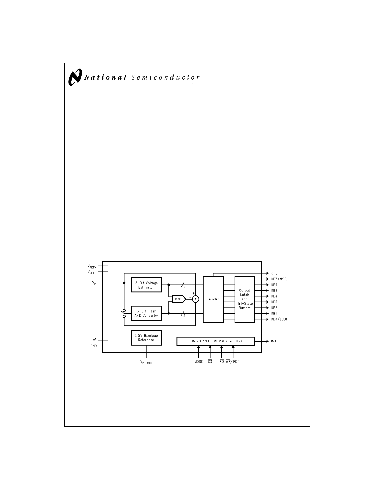
General Description
Using a patented multi-step A/D conversion technique, the
8-bit ADC08161 CMOS A/D converter offers 500 ns conversion time, internal sample-and-hold (S/H), a 2.5V bandgap
reference, and dissipates only 100 mW of power. The
ADC08161 performs an 8-bit conversion with a 2-bit voltage
estimator that generates the 2 MSBs and two low-resolution
(3-bit) flashes that generate the 6 LBSs.
Input signals are tracked and held by the input sampling circuitry, eliminating the need for an external sample-and-hold.
The ADC08161 can perform accurate conversions of
full-scale input signals at frequencies from DC to typically
more than 300 kHz (full power bandwidth) without the need
of an external sample-and-hold (S/H).
For ease of interface to microprocessors, this part has been
designed to appear as a memory location or I/O port without
the need for external interfacing logic.
Block Diagram
Key Specifications
n Resolution 8 Bits
n Conversion time (t
n Full power bandwidth 300 kHz (typ)
n Throughput rate 1.5 MHz min
n Power dissipation 100 mW max
n Total unadjusted error
) 560 ns max (WR-RD Mode)
CONV
1
±
⁄2LSB and±1 LSB max
Features
n No external clock required
n Analog input voltage range from GND to V
n 2.5V bandgap reference
+
Applications
n Mobile telecommunications
n Hard-disk drives
n Instrumentation
n High-speed data acquisition systems
DS011149-1
TRI-STATE®is a registeredtrademark of National Semiconductor Corporation.
© 1999 National Semiconductor Corporation DS011149 www.national.com
Connection Diagram
Wide-Body Small-Outline Package
DS011149-14
See NS Package Number M20B
Ordering Information
Industrial (−40˚C ≤ TA≤ 85˚C) Package
ADC08161CIWM M20B
Pin Description
V
IN
DB0–DB7 TRI-STATE data outputs — bit 0 (LSB)
WR /RDY
MODE Mode: Mode (RD or WR-RD ) selection
RD WR-RD Mode (logic high on the MODE
This is the analog input. The input range is
GND–50 mV ≤ V
≤ V++50mV.
INPUT
through bit 7 (MSB).
WR-RD Mode (Logic high applied to
MODE pin)
WR: With CS low, the conversion is
started on the rising edge of WR. The digital result will be strobed into the output
latch at the end of conversion (
3, 4
).
Figures 2,
RD Mode (Logic low applied to MODE
pin)
RDY: This is an open drain output (no internal pull-up device). RDY will go low after the falling edge of CS and returns high
at the end of conversion.
input– This pin is pulled to a logic low
through an internal 50 µA current sink
when left unconnected.
RD Mode is selected if the MODE pin is
left unconnected or externally forced low.
Acomplete conversion is accomplished by
pulling RD low until output data appears.
WR-RD Mode is selected when a high is
applied to the MODE pin. A conversion
starts with the WR signal’s rising edge and
then using RD to access the data.
pin)
This is the active low Read input. With a
logic low applied to the CS pin, the
TRI-STATE data outputs (DB0–DB7) will
be activated when RD goes low (
2, 3, 4
).
Figures
RD Mode (logic low on the MODE pin)
With CS low, a conversion starts on the
falling edge of RD. Output data appears
on DB0–DB7 at the end of conversion
(
INT
Figures 1, 5
This is an active low output that indicates
).
that a conversion is complete and the data
is in the output latch. INT is reset by the
rising edge of RD.
GND This is the power supply ground pin. The
ground pin should be connected to a
“clean” ground reference point.
V
REF−,VREF+
These are the reference voltage inputs.
They may be placed at any voltage between GND − 50 mV and V
V
must be greater than V
REF+
an input voltage equal to V
an output code of 0, and an input voltage
greater than V
output code of 255.
For the ADC08161 an input voltage that
exceeds V
REF+
+
by more than 100 mV or is be-
+
+50mV,but
. Ideally,
REF−
produces
REF−
− 1.5 LSB produces an
low GND by more than 100 mV will create
conversion errors.
CS
This is the active low Chip Select input. A
logic low signal applied to this input pin enables the RD and WR inputs. Internally,
the CS signal is ORed with RD and WR
signals.
OFL
Overflow Output. If the analog input is
higher than V
end of conversion. It can be used when
, OFL will be low at the
REF+
cascading two ADC08161s to achieve
higher resolution (9 bits). This output is always active and does not go into
TRI-STATE as DB0–DB7 do. When OFL
is set, all data outputs remain high when
+
V
the ADC08061’s output data is read.
Positive powersupply voltage input. Nomi-
nal operating supply voltage is +5V. The
supply pin should be bypassed with a
10 µF bead tantalum in parallel with a 0.1
ceramic capacitor. Lead length should be
as short as possible.
V
REFOUT
The internal bandgap reference’s 2.5V
output is available on this pin. Use a
220 µF bypass capacitor between this pin
and analog ground.
www.national.com 2
Absolute Maximum Ratings (Notes 1, 2)
If Military/Aerospace specified devices are required,
please contact the National Semiconductor Sales Office/
Distributors for availability and specifications.
Supply Voltage (V
Logic Control Inputs −0.3V to V
Voltage at Other Inputs and Outputs −0.3V to V
Input Current at Any Pin (Note 3) 5 mA
Package Input Current (Note 3) 20 mA
Converter Characteristics
The following specifications apply for RD Mode, V
face limits apply for T
+
)6V
=
=
T
A
to T
T
J
MIN
+
+
+
=
; all other limits T
MAX
+ 0.3V
+ 0.3V
5V, V
Power Dissipation (Note 4) 875 mW
Lead Temperature (Note 5)
(Vapor Phase, 60 sec.) +215˚C
(Infrared, 15 sec.) +220˚C
Storage Temperature −65˚C to +150˚C
ESD Susceptibility (Note 6) 750V
Operating Ratings(Notes 1, 2)
Temperature Range T
Supply Voltage, (V
=
5V, and V
REF+
=
T
A
ADC08161CIWM −40˚C ≤ TA≤ 85˚C
=
25˚C.
J
+
) 4.5V to 5.5V
=
GND unless otherwise specified. Bold-
REF−
MIN
≤ TA≤ T
Symbol Parameter Conditions Typical Limits Units
(Note 7) (Note 8) (Limit)
INL Integral Non Linearity V
TUE Total Unadjusted Error (Note 9) V
INL Integral Non Linearity V
TUE Total Unadjusted Error V
Missing Codes V
=
5V
REF
=
5V
REF
=
2.5V
REF
=
2.5V
REF
=
5V 0 Bits (max)
REF
=
V
2.5V 0 Bits (max)
REF
±
1 LSB (max)
±
1 LSB (max)
±
1 LSB (max)
±
1 LSB (max)
Reference Input Resistance 700 500 Ω (min)
700 1250 Ω (max)
V
REF+
V
REF−
V
IN
Positive Reference Input Voltage V
REF−
V
+
V (min)
V (max)
Negative Reference GND V (min)
Input Voltage V
REF+
V (max)
Analog (Note 10) GND − 0.1 V (min)
Input Voltage V
+
+ 0.1 V (max)
On-Channel Input Current On Channel Input=5V,
Off Channel Input=0V −0.4 −20 µA (max)
(Note 11)
On Channel Input=0V,
Off Channel Input=5V −0.4 −20 µA (max)
(Note 11)
+
=
PSS Power Supply Sensitivity V
±
5%,
5V
=
V
4.75V
REF
±
1/16
1
±
⁄
2
LSB (max)
All Codes Tested
Effective Bits V
Full-Power Bandwidth V
THD Total Harmonic Distortion V
S/N Signal-to-Noise Ratio V
IMD Intermodulation Distortion V
C
VIN
Analog Input Capacitance 25 pF
=
4.85 V
IN
=
f
20 Hz to 20 kHz
IN
=
4.85 V
IN
=
4.85 V
IN
=
f
20 Hz to 20 kHz
IN
=
4.85 V
IN
=
f
20 Hz to 20 kHz
IN
=
4.85 V
IN
=
f
20 Hz to 20 kHz
IN
p-p
p-p
p-p
p-p
p-p
7.8 Bits
300 kHz
0.5
%
50 dB
50 dB
MAX
www.national.com3
AC Electrical Characteristics
The following specifications apply for V
limits apply for T
=
=
T
T
A
J
MIN
to T
+
MAX
=
=
5V, t
; all other limits T
=
t
r
f
10 ns, V
=
A
T
REF+
J
=
Symbol Parameter Conditions
t
WR
t
RD
Write Time Mode Pin to V
(
Figures 2, 3, 4
Read Time (Time from Rising Edge Mode Pin to V+,(
+
)
Figure 2
of WR to Falling Edge of RD )
t
RDW
t
CONV
t
CRD
t
ACCO
t
ACC1
t
ACC2
t
1H,t0H
RD Width Mode Pin to GND (
WR -RD Mode Conversion Time Mode Pin to V+,(
(t
WR+tRD+tACC1
)
Figure 2
RD Mode Conversion Time Mode Pin to GND, (
Access Time (Delay from Falling CL≤ 100 pF, Mode Pin to GND 640 900 ns (max)
Edge of RD to Output Valid)
(
Figure 1
)
Access Time (Delay from CL≤ 10 pF 45 ns
Falling Edge of RD
to Output Valid) Mode Pin to V
=
C
100 pF 50 110 ns (max)
L
(
Figure 2
+
,tRD≤ t
)
Access Time (Delay from CL≤ 10 pF 25 ns
Falling Edge of RD
to Output Valid) t
TRI-STATE®Control R
(Delay from Rising Edge (
=
C
100 pF 30 55 ns (max)
L
>
t
=
L
,
INTL
3kΩ,C
)
=
10 pF
L
RD
(
Figures 3, 5
Figures 1, 2, 3, 4, 5
of RD to HI-Z State)
t
t
t
INTL
INTH
INTH
Delay from Rising Edge of Mode Pin=V+,C
WR to Falling Edge of INT
Delay from Rising Edge of C
RD to Rising Edge of INT
Delay from Rising Edge of C
(
Figures 3, 4
L
(
Figures 1, 2, 3, 5
L
)
=
50 pF, 50 95 ns (max)
=
50 pF, (
Figure 4
L
)
WR to Rising Edge of INT
t
RDY
t
ID
t
RI
t
N
Delay from CS to RDY Mode Pin=0V, C
=
R
3kΩ,(
L
Delay from INT R
to Output Valid (
=
3kΩ,C
L
Figure 4
L
Figure 1
=
100 pF 0 15 ns (max)
L
)
Delay from RD to INT Mode Pin=V+,tRD≤ t
(
Figure 2
)
Time between End of RD (
Figures 1, 2, 3, 4, 5
and Start of New Conversion
t
CSS
t
CSH
CS Setup Time (
CS Hold Time (
Figures 1, 2, 3, 4, 5
Figures 1, 2, 3, 4, 5
=
25˚C.
5V, V
=
0V unless otherwise specified. Boldface
REF−
Typical
(Note 7)
Limit
(Note 8)
Units
(Limit)
100 100 ns (min)
) 350 350 ns (min)
Figure 5
) 200 250 ns (min)
400 400 ns (max)
) 500 560 ns (max)
Figure 1
) 655 900 ns (max)
INTL
)3060 ns (max)
=
50 pF 520 690 ns (max)
)4595 ns (max)
=
50 pF, 25 45 ns (max)
)
INTL
60 115 ns (max)
)5050 ns (min)
)00ns (max)
)00ns (max)
DC Electrical Characteristics
The following specifications apply for V
all other limits T
=
=
T
25˚C.
A
J
+
=
5V unless otherwise specified. Boldface limits apply for T
Symbol Parameter Conditions
+
V
Logic “1” Input Voltage V
IH
=
5.5 V
CS, WR, RD, A0, A1, A2 Pins
Mode Pin 3.5
www.national.com 4
Typical
(Note 7)
=
=
T
A
Limit
(Note 8)
to T
T
J
MIN
2.0 V (min)
MAX
Units
(Limit)
;
DC Electrical Characteristics (Continued)
+
The following specifications apply for V
all other limits T
=
=
T
25˚C.
A
J
Symbol Parameter Conditions
V
I
I
V
V
I
I
I
I
C
C
Logic “0” Input Voltage V
IL
Logic “1” Input Current V
IH
Logic “0” Input Current V
IL
Logic “1” Output Voltage V
OH
Logic “0” Output Voltage V
OL
TRI-STATE Output Current V
O
Output Source Current V
SOURCE
Output Sink Current V
SINK
Supply Current CS=WR=RD=0 11.5 20 mA (max)
C
Logic Output Capacitance 5 pF
OUT
Logic Input Capacitance 5 pF
IN
=
5V unless otherwise specified. Boldface limits apply for T
+
=
4.5V
CS, WR, RD, A0, A1, A2 Pins
Mode Pin 1.5
=
5V
H
CS, RD, A0, A, A2 Pins
WR Pin
Mode Pin 50 200
=
0V
L
CS, RD, WR, A0, A1, A2
Mode Pins −0.005 −2 µA (max)
+
=
4.75V
=
I
−360 µA 2.4 V (min)
OUT
DB0–DB7, OFL, INT
=
I
−10 µA 4.5 V (min)
OUT
DB0–DB7, OFL, INT
+
=
4.75V
=
I
1.6 mA 0.4 V (max)
OUT
DB0–DB7, OFL, INT, RDY
=
5.0V 0.1 3 µA (max)
OUT
DB0–DB7, RDY
=
V
0V −0.1 −3 µA (max)
OUT
DB0–DB7, RDY
=
0V −26 −6 mA (min)
OUT
DB0–DB7, OFL, INT
=
5V 24 7 mA (min)
OUT
DB0–DB7, OFL, INT, RDY
=
=
to T
T
J
MIN
(Limit)
Typical
(Note 7)
T
A
Limit
(Note 8)
0.8 V (max)
0.005 1
0.1 3 µA (max)
MAX
Units
;
Bandgap Reference Electrical Characteristics
The following specifications apply for V
=
limits T
=
T
25˚C.
A
J
+
=
5V unless otherwise specified. Boldface limits apply for T
MIN
to T
MAX
; all other
Symbol Parameter Conditions Typical Limits Units
(Note 7) (Note 8) (Limit)
V
REFOUT
∆V
REF
Internal Reference Output Voltage 2.5±2.0
/∆T Internal Reference Temperature 40 ppm/˚C
%
V (max)
Coefficient
∆V
/∆ILInternal Reference Load Sourcing (0 ≤ IL≤ +10 mA) 0.01 0.1
REF
%
/mA (max)
Regulation
Line Regulation 4.75V ≤ V
I
∆V
SC
REF/∆t
Short Circuit Current V
Long Term Stability 200 ppm/kHr
Start-Up Time V
Note 1: Absolute Maximum Ratings indicate limits beyond which damage to the device may occur. DC and AC electrical specifications do not apply when operating
the device beyond its specified operating ratings. Operating Ratings indicate conditions for which the device is functional, but do not guarantee performance limits.
For guaranteed specifications and test conditions, see the Electrical Characteristics. The guaranteed specificationsapply only for the test conditions listed. Some performance characteristics may degrade when the device is not operated under the listed test conditions.
+
≤ 5.25V 0.5 6.0 mV (max)
=
0V 35 mA (max)
REV
+
:0V→5V, C
=
220 µF 40 ms
L
www.national.com5
 Loading...