

Page 1
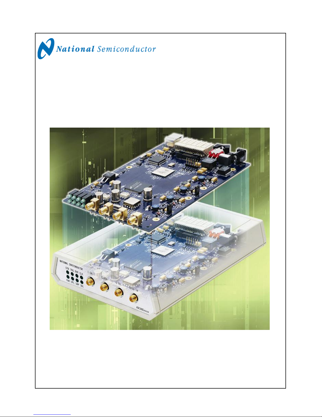
March 24, 2006
Revision A
Development Board Instruction Manual
ADC081500DEV - Single 8-Bit, 1.5 GSPS, 1.2W A/D Converter with
Xilinx Virtex 4 (XC4VLX15) FPGA
© Copyright 2006 National Semiconductor Corporation
1 www.national.com
Page 2

ADC081500EVAL BOARD USER MANUAL – TABLE OF CONTENTS
ADC081500EVAL BOARD USER MANUAL – TABLE OF CONTENTS........................2
1.0 Introduction........................................................................................................................... 3
2.0 Board Assembly.................................................................................................................... 3
3.0 Quick Start............................................................................................................................ 4
4.0 Functional Description .......................................................................................................... 4
4.1 Input circuitry...................................................................................................................... 4
4.2 ADC reference.................................................................................................................... 4
4.3 ADC clock........................................................................................................................... 4
4.4 Digital Data Output............................................................................................................. 4
4.5 Power Requirements..........................................................................................................5
4.6 Power Supply Connections................................................................................................ 5
5.0 Obtaining Best Results ......................................................................................................... 5
5.1 Clock Jitter.......................................................................................................................... 5
6.0 Evaluation Board Specifications ........................................................................................... 5
7.0 Schematic Drawing ADC081500DEV – Onboard Clock (VCO + PLL) ................................. 6
7.1 Schematic Drawing ADC081500DEV – Analog Inputs (I,Q) & Digital Trigger Input........... 7
7.2 Schematic Drawing ADC081500DEV – ADC connected to Virtex4 FPGA ........................ 8
7.3 Schematic Drawing ADC081500DEV – USB Interface...................................................... 9
7.4 Schematic Drawing ADC081500DEV – Power Supplies 1 .............................................. 10
7.5 Schematic Drawing ADC081500DEV – Power Supplies 2 .............................................. 11
7.6 Schematic Drawing ADC081500DEV – Expansion Header Interface.............................. 12
8.0 Bill of Materials (Page 1 of 2)..............................................................................................13
8.1 Bill of Material (Page 2 of 2)............................................................................................. 14
9.0 Using the Wavevision4 software with the ADC081500DEV ............................................... 15
9.1 Getting Started................................................................................................................. 15
9.2 Control Panel.................................................................................................................... 17
9.3 Serial Control Mode.......................................................................................................... 19
9.4 Capturing Waveforms....................................................................................................... 20
10.0 Appendix A - Hardware Information.................................................................................. 20
10.1 LED functions................................................................................................................. 20
10.2 Expansion Header.......................................................................................................... 21
10.3 System Block Diagram................................................................................................... 22
11.0 Appendix B - Installing and running the Wavevision 4 software....................................... 23
11.1 Install the WaveVision Software..................................................................................... 23
11.2 Java™ Technology......................................................................................................... 23
11.3 Automatic Device Detection & Configuration ................................................................. 23
11.4 Windows Driver.............................................................................................................. 23
12.0 Appendix C - Using WaveVision Plots.............................................................................. 24
The Waveform Plot................................................................................................................. 24
The FFT Plot .......................................................................................................................... 24
FFT Options ........................................................................................................................... 25
Histogram Plots...................................................................................................................... 26
Information Viewer ................................................................................................................. 26
Data Import and Export..........................................................................................................26
2 www.national.com
Page 3
1.0 Introduction
The ADC081500DEV Board is designed to
allow quick evaluation and design development
of National Semiconductor’s ADC081500 8-bit
Analog-to-Digital Converter. This device is
specified for 1.5 GSPS operation.
This development board is designed to function
with National Semiconductor’s WaveVision
Software, for fast evaluation. It requires only 3
connections to get started: a Power Supply, a
USB Interface to PC and a Signal Source. A
1.5GHz Clock generator is provided on board
and the system also allows an external clock to
be used if alternative sample rates are required.
Analog I Channel
Input
Clock Input
The ADC connects to a Xilinx Virtex4 FPGA
which stores up to 4K of data from each
channel before transferring it through the USB
interface to the PC.
2.0 Board Assembly
The ADC081500 Development Board comes in
a low profile plastic enclosure and requires no
assisted cooling due to its low power
consumption. The ADC081500 device is
configured entirely through software and also
allows changes to easily be made to the FPGA
configuration to enable system development.
USB
E
x
p
a
n
s
i
o
n
Trigger Input
PWR
SWITCH
PWR
INPUT
Figure 1 Component Placement & Front Panel
3 www.national.com
Page 4

3.0 Quick Start
Refer to Figure 1 for locations of the power
connection, signal input and USB port.
IMPORTANT NOTE:
Install the Wavevision 4 Software before
connecting this product to the PC. See
Appendix B – Installing Wavevision.
For quick start operation:
1. Connect the 12V DC power source
(included with the development board) to the
rear Power Connector labeled (8-12V DC).
2. Connect a stable sine wave source capable
of supplying the desired input frequencies at
up to 8 dBm. Connect this signal to the front
panel SMA connector labeled “I CH.”
through a band pass filter. The exact level
needed from the generator will
depend upon
the insertion loss of the filter used.
3 Connect the USB cable (included) from the
USB port to the PC. If this is the first time
the board has been connected, Windows
may install the drivers for this product at this
time.
5. Push the Power Switch to the ON position
on the rear panel and check that the Green
LED between the switch and the power
connector illuminates.
6. Start the Wavevision 4 Software
7. Once loaded the “Firmware Download”
Progress bar should be displayed. See
Appendix B for more information.
8. Upon Firmware Download completion, the
control panel for the board should
automatically be displayed on the PC and
the CLK LED on the front panel should be
flashing.
8. Set the signal source for the analog input to
8 dBm at the desired frequency. Observe
the ‘Out of Range’ LED “OVR” on the front
panel is illuminated. If this LED is not on,
increase the input signal source until it is.
9. Reduce the input level until the ‘OVR’ LED
just turns off.
10. From the Wavevision 4 pull-down menu
select “Acquire” and then samples. The
system will then capture the input waveform
and display the results in the time domain.
11. For FFT Analysis click the FFT Tab.
4.0 Functional Description
The ADC081500 Development Board schematic
is shown in Section 7.0.
4.1 Input circuitry
The input signal(s) to be digitized should be
applied to the front panel SMA connectors
labeled “I CH.” and “Q CH.”. These 50 Ohm
inputs are intended to accept a low-noise sine
wave signals. To accurately evaluate the
dynamic performance of this converter, the input
test signals will have to be passed through a
high-quality bandpass filter with at least 10-bit
equivalent noise and distortion characteristics.
This evaluation board as delivered is set up for
operation with two single-ended analog inputs,
which are converted to differential signals on
board.
Signal transformer T2, is connected as a balun,
and provides the single-ended to differential
conversion. The differential PCB traces to the
ADC analog input pins have a characteristic
differential impedance of 100 Ohms.
No scope or other test equipment should be
connected anywhere in the signal path while
gathering data.
4.2 ADC reference
The ADC081500 has an internal reference that
can not be adjusted. However, the Full-Scale
(differential) Range may adjusted with the
Software Control Panel Refer to Section 9.0 for
more information
4.3 ADC clock
The ADC clock is supplied on board and is fixed
at 1.5GHz. An external clock signal may be
applied to the ADC through the SMA Connector
labeled “CLOCK” on the front panel. The baluntransformer (T1) converts the single ended clock
source to a differential signal to drive the ADC
clock pins
Note that it is very important that the ADC clock
should be as free of jitter as possible or the
apparent SNR of the ADC081500 will be
compromised.
4.4 Digital Data Output
The digital output data from the ADC081500 is
connected to a Xilinx 4 FPGA. Up to 4K Bytes of
data can be stored and then uploaded over the
USB interface to the Wavevision 4 software. The
FPGA logic usage is low allowing further code to
be written and tested for product development.
4 www.national.com
Page 5

4.5 Power Requirements
The power supply requirement for the
ADC081500 Evaluation Board is 12V at 800mA.
Most of the regulators on board are switching
regulators for increased power efficiency.
The board typically draws around 500mA but it
is always good practice to have extra power
reserve in the power supply over the typical
power requirements.
A Universal 100-240V AC input to 12V DC Brick
Power Supply is included with the development
board.
4.6 Power Supply Connections
Power to this board is supplied through the
power connector on the rear panel. It is advised
that only the supplied PSU is used with this
board.
The ADC081500 supply voltage has been set to
1.9V, ±50 mV.
5.0 Obtaining Best Results
Obtaining the best results with any ADC
requires both good circuit techniques and a
good PC board layout. For layout information for
this product please contact you nearest National
Semiconductor representative
5.1 Clock Jitter
When any circuitry is added after a signal
source, some jitter is almost always added to
that signal. Jitter in a clock signal, depending
upon how bad it is, can degrade dynamic
performance. We can see the effects of jitter in
the frequency domain (FFT) as "leakage" or
"spreading" around the input frequency, as seen
in Figure 2a. Compare this with the more
desirable plot of Figure 2b. Note that all dynamic
performance parameters (shown to the right of
the FFT) are improved by eliminating clock jitter.
.
Figure 2a. Jitter causes a spreading around the input
signal, as well as undesirable signal spurs.
Figure 2b. Eliminating or minimizing clock jitter results in
a more desirable FFT that is more representative of how
the ADC actually performs.
6.0 Evaluation Board
Specifications
Board Size: 168mm x 100mm
Power Requirements: +12V, 800mA
Clock Frequency Range : 200 MHz to 1.5 GHz
Analog Input Range (AC Coupled) 30MHz to 1800MHz
Nominal Analog Input Voltage: 560 mV P-P to 870 mV P-P
Impedance: 50 Ohms
5 www.national.com
Page 6

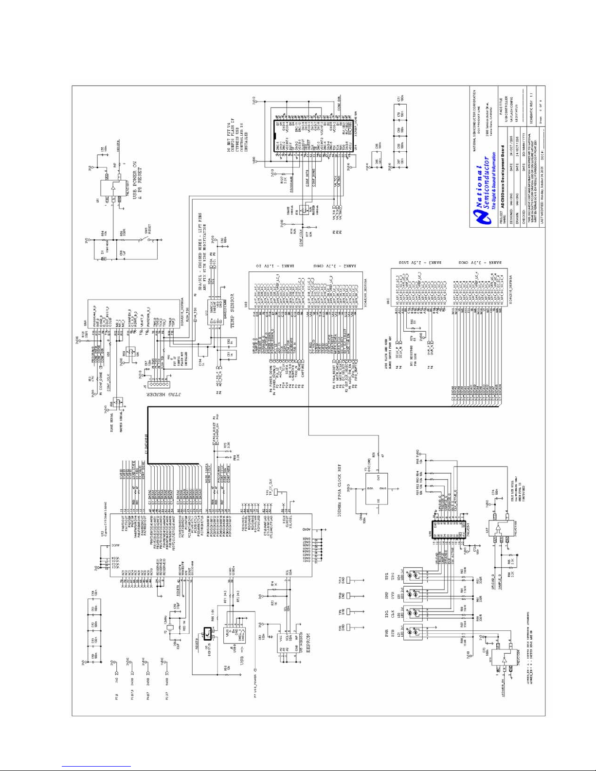
7.0 Schematic Drawing ADC081500DEV – Onboard Clock (VCO + PLL)
6 www.national.com
Page 7
7.1 Schematic Drawing ADC081500DEV – Analog Inputs (I,Q) & Digital Trigger Input
7 www.national.com
Page 8
7.2 Schematic Drawing ADC081500DEV – ADC connected to Virtex4 FPGA
8 www.national.com
Page 9
7.3 Schematic Drawing ADC081500DEV – USB Interface
9 www.national.com
Page 10

7.4 Schematic Drawing ADC081500DEV – Power Supplies 1
10 www.national.com
Page 11

7.5 Schematic Drawing ADC081500DEV – Power Supplies 2
11 www.national.com
Page 12

7.6 Schematic Drawing ADC081500DEV – Expansion Header Interface
12 www.national.com
Page 13

8.0 Bill of Materials (Page 1 of 2)
13 www.national.com
Page 14

8.1 Bill of Material (Page 2 of 2)
14 www.national.com
Page 15

9.0 Using the Wavevision4 software with the ADC081500DEV
IMPORTANT NOTE: Before connecting this board to the PC, please install the Wavevision 4
Software from the CDROM included with the development kit. (See Appendix B)
Connecting the Development Board before installation may result in the board being registered as
an unknown USB device. If this happens you will need to uninstall the device using the Windows
Device Manager before installing the Wavevision 4 Software.
9.1 Getting Started
This development board is designed to connect over a USB interface to a PC running the Wavevision 4
Software.
Ensure the board is connected to the 12V power supply (included in the package) and that the switch on
the rear panel is pushed to the “ON” position. The Green LED on the rear panel should be illuminated
Connect the USB cable between the PC which has Wavevision 4 software installed and the
ADC081500DEV board. The USB port can also be found on the rear panel (shown below).
If this is the 1
(automatic) by the Operating System. Follow the on screen instructions and use the recommended
settings.
st
time the board has been connected to the PC, Drivers may be required to be installed
Start the Wavevision 4 software (Start -> All Programs -> Wavevision -> Wavevision 4)
The software may take several seconds to initialize, but should display a welcome screen similar to the
following.
15 www.national.com
Page 16

If the board is connected correctly the following popup box should appear to indicate that the board has
been recognized and the firmware for the FPGA is being downloaded over the USB interface
If the “Downloading firmware” box does not appear automatically, click on the “Settings” pulldown menu
and then click Capture Settings as shown below.
This will display the System Settings Window which should appear as below
If the board has not been detected click the “Test” button under the Communication heading and the
development board should be found. If the communications fail, check that the USB drivers are installed
correctly, then disconnect and re-connect the USB cable. Finally restart the Wavevision 4 software See
Appendix B for more information.
16 www.national.com
Page 17

9.2 Control Panel
Once the FPGA Firmware download has completed the development board Control Panel will
automatically be displayed as shown below.
The Following section describes the Function of the pull-down selection tabs in the left hand side of the
ADC081500DEV product Control Panel
Channel Selection
I – Displays the data captured from the I Channel Only after acquiring Samples
Q- Display is not available on this board due to the ADC being single channel
I and Q – Display is not a valid selection
I/Q Interleaved – is not a valid selection
Temp Sensor
Displayed below the Channel Selection tab is the die temperature of both the FPGA and the ADC
Hardware/Serial Control
Hardware Pin Control – The ADC is controlled by the logic states on the dedicated control pins. The logic
on these pins is determined by the setting of OUTV, OUTEDGE, DDR, DES and FSR below.
Serial Register Program – The ADCs registers are accessed through the Extended Control Mode. In this
mode the hardware pin control is disabled and the programmable registers are available for fine tuning.
17 www.national.com
Page 18

Out V
Low Amplitude – LVDS output voltage amplitude is set to 510mV pk-pk
High Amplitude – LVDS output voltage amplitude is set to 710mV pk-pk
OutEdge
Falling Edge – Data outputs are changed on the falling edge of DCLK+ (Single Data rate mode only)
Rising Edge – Data output are changed on the rising edge of DCLK+ (Single Data rate mode only)
DDR
Disable Dual Data Rate – DDR Mode is disabled (data output follows OutEdge Setting)
Enable Dual Data Rate – Data is output with rising and falling edge of DCLK (Default for 1.5GHz clock)
DES
Disable Dual Edge Sample – DES Mode is disabled.
Enable Dual Edge Sample – This Feature is not available on the single channel device
FSR
650mV Full Scale – Sets the full scale range to 650mV pk-pk
870mV Full Scale – Sets the full scale range to 870mV pk-pk
The Following Pull-down Tabs are available whether the Control mode is Hardware or Serial
Standby
Disable Standby – Enable all on-board power regulators
Enable Standby – Board is put into standby mode – All power is shutdown except USB power
PDQ
Disable Q Shutdown – Q Channel is not available
Enable Q Shutdown – Q Channel is not available
PD
Disable Shutdown – The ADC is powered up and Active
Enable Shutdown – The ADC is put into low power mode. Register Settings are retained
DC_Coup
AC Coupling – The I Channel is AC coupled to the ADCs input
DC Coupling – The I Channel is DC coupled to the ADCs input (not available on AC only model)
Ext_Clock
Internal Clock – The ADC is clocked using the on-board 1.5GHz clock
External Clock – The ADC is clocked from an External clock source connected to the “CLOCK” input.
18 www.national.com
Page 19

Reset FPGA
This button resets the FPGA, and also returns all the pulldown tabs to their default values
Calibrate ADC
This button issues an on-command calibration to the ADC by toggling the ADCs calibrate pin.
9.3 Serial Control Mode
When the Hardware/Serial Control tab is selected as “Serial Register Program”, the control panel display
will be changed to the following view.
In this mode the register settings can be changed simply by clicking on the bits. Doing so will toggle the bit
value and any linear values such as Full Scale Range or Offset will automatically be updated.
The “Reset Registers” button at the bottom of the Control Panel will reset and write all the values to the
power-on default settings.
Please refer to the ADC081500 datasheet for a full description of the ADCs internal registers.
19 www.national.com
Page 20

9.4 Capturing Waveforms
When the ADC has been configured as required, the selected input(s) can be sampled by clicking the
“Acquire” pull-down menu and selecting “Samples”. Alternatively press F1 then the Escape key.
10.0 Appendix A - Hardware Information
10.1 LED functions
The function of the LEDs on the front panel of the boards is as follows
STB – STANDBY, Illuminates when the board is in standby mode.
TRG – TRIGGER EVENT, illuminates when the Trigger Input makes low to high transition
OVR – ADC OVER RANGE, Illuminates when the I or Q channel exceeds the full scale range of the ADC
CLK – CLOCK INPUT, flashes with 50% duty cycle if the ADC is receiving a good clock input.
PWR – POWER, illuminates when the external 12V is connected, and the system is not in Standby.
UPL – UPLOAD, illuminates when the FPGA is uploading sample data to the PC
SMP – SAMPLE, illuminates when the FPGA is sampling data and storing to the FIFO buffers
IDL – IDLE, Illuminates when the system is IDLE.
20 www.national.com
Page 21

10.2 Expansion Header
A 72 pin Future Bus Expansion Header is provided on the rear panel to allow easy connection to a third
party microprocessor board to allow for the reading and analysis of the data captured by the FPGA.
The signals connector to this expansion bus will be as follows
PIN DESCRIPTION PIN DESCRIPTION
A1 I2C - SDA B1 GROUND
A2 I2C - SCL B2 GROUND
A3 SSP - SERIAL DATA B3 GROUND
A4 SSP - SERIAL CLOCK B4 GROUND
A5 FPGA RESET B5 GROUND
A6 READ FIFO B6 GROUND
A7 WRITE FIFO B7 GROUND
A8 FIFO FULL B8 GROUND
A9 FIFO EMPTY B9 GROUND
A10 ADC DCLK RESET B10 GROUND
A11 FPGA CONF DONE B11 GROUND
A12 FPGA JTAG – TMS B12 GROUND
A13 FPGA JTAG - TCK B13 GROUND
A14 FPGA JTAG – TDI B14 GROUND
A15 FPGA JTAG – TDO B15 GROUND
A16 notSHUTDOWN B16 GROUND
A17 3.3V SUPPLY B17 GROUND
A18 12V SUPPLY B18 GROUND
C1 DATA BUS A P0 (LVDS or CMOS) D1 DATA BUS A N0 (LVDS or CMOS)
C2 DATA BUS A P1 (LVDS or CMOS) D2 DATA BUS A N1 (LVDS or CMOS)
C3 DATA BUS A P2 (LVDS or CMOS) D3 DATA BUS A N2 (LVDS or CMOS)
C4 DATA BUS A P3 (LVDS or CMOS) D4 DATA BUS A N3 (LVDS or CMOS)
C5 DATA BUS A P4 (LVDS or CMOS) D5 DATA BUS A N4 (LVDS or CMOS)
C6 DATA BUS A P5 (LVDS or CMOS) D6 DATA BUS A N5 (LVDS or CMOS)
C7 DATA BUS A P6 (LVDS or CMOS) D7 DATA BUS A N6 (LVDS or CMOS)
C8 DATA BUS A P7 (LVDS or CMOS) D8 DATA BUS A N7 (LVDS or CMOS)
C9 INPUT STROBE P D9 INPUT STROBE N
C10 DATA BUS B P0 (LVDS or CMOS) D10 DATA BUS B N0 (LVDS or CMOS)
C11 DATA BUS B P1 (LVDS or CMOS) D11 DATA BUS B N1 (LVDS or CMOS)
C12 DATA BUS B P2 (LVDS or CMOS) D12 DATA BUS B N2 (LVDS or CMOS)
C13 DATA BUS B P3 (LVDS or CMOS) D13 DATA BUS B N3 (LVDS or CMOS)
C14 DATA BUS B P4 (LVDS or CMOS) D14 DATA BUS B N4 (LVDS or CMOS)
C15 DATA BUS B P5 (LVDS or CMOS) D15 DATA BUS B N5 (LVDS or CMOS)
C16 DATA BUS B P6 (LVDS or CMOS) D16 DATA BUS B N6 (LVDS or CMOS)
C17 DATA BUS B P7 (LVDS or CMOS) D17 DATA BUS B N7 (LVDS or CMOS)
C18 OUTPUT STROBE P D18 OUTPUT STROBE N
The Data busses on this header can be configured as follows
• Two 8 bit busses with LVDS differential signaling, plus two LVDS strobes
• Four 8 bit busses with LVCMOS (3.3V IO) signaling plus four CMOS strobes
All control signals on pins A1 to A15 will be at LVCMOS 3.3V levels.
21 www.national.com
Page 22

10.3 System Block Diagram
22 www.national.com
Page 23

11.0 Appendix B - Installing and running the Wavevision 4 software
11.1 Install the WaveVision Software.
• Insert the WaveVision CD-ROM into your computer’s CD-ROM drive.
• The WaveVision software requires a Java™ Runtime Environment or Java™ Development Kit,
version 1.4 or higher, from Sun Microsystems, Inc. For detailed information on WaveVision’s use
of Java technology, please see below. If your computer does not have this software, the
WaveVision installer will instruct you on how to install it.
• Locate and run the WaveVision 4 Setup.exe program on the CD-ROM. Follow the on-screen
instructions to finish the install
11.2 Java™ Technology
The WaveVision software uses Sun Microsystems® Java technology. The underlying Java software must
be installed on your computer in order for the WaveVision software to run. The software can run on top of
either the Java Runtime Environment (JRE) or the Java Development Kit (JDK), version 1.4 or higher. A
suitable copy of the JRE is included on your WaveVision CD-ROM.
The WaveVision installer will first look for an existing copy of the JRE or JDK on your computer. If neither
is found, the installer will instruct you to first install a JRE. To do this, run the J2RE*.exe installer
program off the CD-ROM. Follow the on-screen instructions to finish the install.
After a suitable JRE or JDK is installed, run the WaveVision installer again. The installer will detect the
Java software and configure the WaveVision software to use it.
Java technology can allow software to run on different platforms. However, the WaveVision software
contains Windows specific hardware interface code and therefore is only currently supported under
Windows.
.
11.3 Automatic Device Detection & Configuration
The WaveVision system provides automatic hardware detection and configuration for the device under
test. The FPGA is re-programmed on the fly by the host PC when the Development board is turned on.
Normally, the configuration process is totally transparent to the user, and requires no intervention.
However, this process can be overridden if required by specifying a new Xilinx configuration image by
clicking the Xilinx Image Settings button within the Capture Setting window (Settings -> Capture Settings).
11.4 Windows Driver
The WaveVision software communicates with the WaveVision hardware through the Windows device
driver software. If you are unable to connect to the Wavevision board after installing the software, do the
following to uninstall and reinstall the driver. Go to the Windows Control Panel and select System. If you
are using Windows 2000/XP select the Hardware tab. Then click on Device Manager and go down to the
Universal Serial Bus controllers. With the WaveVision board connected, you will see it (or an unknown
device) listed. Right click on it and uninstall the driver. Then unplug and plug in the board again to reinstall
the driver
.
23 www.national.com
Page 24

12.0 Appendix C - Using WaveVision Plots
The WaveVision software provides several tools to help you interact with plots. A toolbar appears above
each plot, similar to Figure 4.
Figure 4: WaveVision Plot Tools
Seen from left to right, the following tools are available:
Plot Actions menu: This menu contains commands that pertain to this particular plot. You may export
the plot data to a file, print the plot, save it as a graphic, or change the plot’s colors.
Plot Options: This button opens a dialog box with options that pertain to this particular plot. You may turn
off labels, annotations, or other elements in this dialog. The WaveVision software maintains default
options for new plots. You may edit the default options by choosing Default Plot Options from the
Settings menu.
FFT Options: The toolbar shown in Figure 4 is from an FFT plot, and thus contains a button to edit the
options for the FFT calculation. Depending upon the type of plot, various options may be present on the
toolbar. Please consult the appropriate section below for more information about these options.
Magnifying glass tool: This tool allows you to zoom in and out to see fine details in the plot. Click and
drag a box from upper-left to lower-right to zoom in on a particular region of your plot. Click and drag a
box from lower-right to upper-left to zoom out. With the magnifying glass tool selected, click the right
mouse button to return to a normal, 100% view.
Arrow Tool: The arrow tool is used to select, move, and edit annotations. To edit an annotation, double
click it with the arrow tool. To delete an annotation, select it with the arrow tool and press the Delete key
on your keyboard.
Line Annotation Tool: To draw lines on the plot, select this tool. Drag to draw new lines. To add
arrowheads, or fix the endpoints of the line, double-click it with the arrow tool.
Text Annotation Tool: To draw labels on the plot, select this tool and click at the desired location in the
plot. To edit the justification, location, or text of an annotation, double-click it with the arrow tool.
The Waveform Plot
The Waveform plot shows you the raw samples collected from the hardware. This plot is mainly used to
verify the integrity of collected data – the waveform is the best view in which to diagnose a distorted signal,
an irregular clock, a low-amplitude signal, and many other common ADC system problems.
The Waveform plot also quickly shows you how much of the ADC’s dynamic range your signal occupies.
The FFT Plot
The WaveVision software automatically computes a Fast Fourier Transform (FFT) of the sample set, and
displays the results in an FFT plot. The FFT plot is, in many respects, the heart of the software. The FFT
shows you the frequency content of your input signal. It marks the fundamental frequency, and a
selectable number of harmonics. It also labels their order and frequencies. It shows the power in the
fundamental and harmonics. Try hovering your mouse cursor over a harmonic to get information about it.
The FFT can be used to diagnose common ADC problems such as input spectral impurity, clock phase
noise, and clock jitter. The FFT plot also shows several statistics on the quality and purity of the collected
24 www.national.com
Page 25

samples, such as SNR, SINAD, THD, SFDR, and ENOB. These statistics are to be interpreted with the
following definitions (which are repeated in every National Semiconductor ADC datasheet):
Signal to Noise Ratio (SNR) is the ratio, expressed in dB, of the RMS value of the input signal to the
RMS value of the sum of all other spectral components below one-half the sampling frequency, not
including harmonics or DC.
Signal to Noise Plus Distortion (S/N+D or SINAD) Is the ratio, expressed in dB, of the RMS value of the
input signal to the RMS value of all of the other spectral components below half the clock frequency,
including harmonics but excluding DC.
Total Harmonic Distortion (THD) is the ratio, expressed in dBc, of the RMS total of the first five harmonic
levels at the output to the level of the fundamental at the output. THD is calculated as
22
ff
log20THD
2
++=L
N
2
f
1
where f
is the RMS power of the fundamental (output) frequency and f2 through fN are the RMS power in
1
the first N harmonic frequencies.
Spurious-Free Dynamic Range (SFDR) is the difference, expressed in dB, between the RMS values of
the input signal and the peak spurious signal, where a spurious signal is any signal present in the output
spectrum that is not present at the input.
Effective Number of Bits (ENOB, or Effective Bits) is another method of specifying Signal-to-Noise and
Distortion or SINAD. ENOB is defined as (SINAD - 1.76) / 6.02 and says that the converter is equivalent to
a perfect ADC of this (ENOB) number of bits.
FFT Options
FFT plots can be configured in many different ways. Clicking the “FFT Options” button at the top of the
plot will display a dialog showing the options for that particular plot. The software also maintains default
options for new FFT plots, which are editable. You can edit the default FFT options by choosing Default
FFT Options from the Settings menu. The options are:
Windowing: You may choose from one of five different window functions. The window function is applied
to the samples before computing the FFT to compensate for the fact that the sample set may not be an
integral number of wavelengths of the input signal. In general, Flat-Top will give the best results, but you
may find it easier to compare data with other systems when the windowing functions are the same.
dB Scale: You may select to represent power on the FFT in dBc (decibels relative to carrier), in which 0
dB is taken to be the fundamental (carrier) power, or dBFS (decibels relative to full-scale), in which 0 dB is
taken to the be power contained in a signal which uses the entire dynamic range of the ADC.
Harmonics: You may select the number of harmonics recognized (and labeled) by the software. You may
also select the number of FFT bins excluded around harmonics in, for example, SNR calculations. The
exclusion region around each harmonic will be shown in a different color than the rest of the data points.
IMD Calculations: The WaveVision software is capable of performing Intermodulation Distortion
calculations. When two fundamental frequencies within 3 dBFS are present in the waveform, The
software will normally perform IMD calculations. You may inhibit this behavior by deselecting the “Allow
IMD calculation” checkbox. When IMD calculation is enabled, you may also select whether the software
will include only 2
nd
order or both 2nd and 3rd order terms.
25 www.national.com
Page 26

Histogram Plots
Histogram plots are created by counting the number of times each ADC output code appears in a dataset.
Histograms may be computed by software, or by hardware. A software histogram is computed from a
dataset which is normally 128k samples or smaller. A hardware histogram is collected directly by the
hardware, and may include millions of counts per code. The resulting histogram will show discontinuities
between comparators, gain or offset errors, and other common ADC system problems.
The Histogram plot also displays the number of codes that were never counted (missing codes), followed
by the first ten such missing codes.
Information Viewer
The information viewer is not a plot, but it displays a variety of useful information about the dataset, such
as the sampling rate, and any warnings generated by the software. You may also store comments about
the dataset here, to be saved in a WaveVision file.
Data Import and Export
The WaveVision software provides a variety of means to share data with others, in both textual and
graphical formats.
The most flexible way to import data into the software is from a tab-delimited ASCII text file. The contents
can be either a sample set or a histogram, provided with or without time information. The simplest
example of this would be a file with a single column of samples. You can open tab-delimited text files by
choosing Open from the File menu; you can interleave data from multiple columns and/or files. You can
choose ReOpen to reopen the same file later with the same settings (for example when you update the file
with new data),
There are a variety of ways to export data from the software:
• Save the file as a normal WV4 (*.wv4) file. WV4 files are ASCII, tab-delimited text files. Samples
are stored one per line in a single column. You can open a WV4 file directly in a spreadsheet
program.
• Save the file as a TXT (*.txt) file. You will produce a one- or two-column tab-delimited ASCII text
file of samples or histogram information, without the header information that is contained in a WV4
file.
• You can export the contents of an individual plot by choosing Export Data… from the plot’s
Plot Actions menu. The format of the data is always tab-delimited ASCII text.
• You can export a plot as either a GIF (*.gif) or Encapsulated Postscript (*.eps) graphic by
choosing Export Plot as Graphic from the plot’s Plot Actions menu. GIF files are
suitable for the web or for emails. Encapsulated Postscript files are high-resolution scalable files
suitable for direct publication.
26 www.national.com
Page 27

BY USING THIS PRODUCT, YOU ARE AGREEING TO BE BOUND BY THE TERMS AND CONDITIONS OF NATIONAL
SEMICONDUCTOR'S END USER LICENSE AGREEMENT. DO NOT USE THIS PRODUCT UNTIL YOU HAVE READ AND
AGREED TO THE TERMS AND CONDITIONS OF THAT AGREEMENT. IF YOU DO NOT AGREE WITH THEM, CONTACT THE
VENDOR WITHIN TEN (10) DAYS OF RECEIPT FOR INSTRUCTIONS ON RETURN OF THE UNUSED PRODUCT FOR A
REFUND OF THE PURCHASE PRICE PAID, IF ANY.
The ADC081500DEV Development Boards are intended for product evaluation purposes only and are not intended for resale to end
consumers, is not authorized for such use and is not designed for compliance with European EMC Directive 89/336/EEC, or for
compliance with any other electromagnetic compatibility requirements.
National Semiconductor Corporation does not assume any responsibility for use of any circuitry or software supplied or described. No
circuit patent licenses are implied
.LIFE SUPPORT POLICY
NATIONAL'S PRODUCTS ARE NOT AUTHORIZED FOR USE AS CRITICAL COMPONENTS IN LIFE SUPPORT DEVICES OR
SYSTEMS WITHOUT THE EXPRESS WRITTEN APPROVAL OF THE PRESIDENT OF NATIONAL SEMICONDUCTOR
CORPORATION. As used herein:
1. Life support devices or systems are devices or
systems which, (a) are intended for surgical implant into the
body, or (b) support or sustain life, and whose failure to
perform, when properly used in accordance with instructions
2. A critical component is any component in a life support
device or system whose failure to perform can be reasonably
expected to cause the failure of the life support device or
system, or to affect its safety or effectiveness.
for use provided in the labeling, can be reasonably expected
to result in a significant injury to the user.
BANNED SUBSTANCE COMPLIANCE
National Semiconductor certifies that the products and packing materials meet the provisions of the Customer
Products Stewardship Specification (CSP-9-111C2) and the Banned Substances and Materials of Interest
Specification (CSP-9-111S2) and contain no ‘‘Banned Substances’’ as defined in CSP-9-111S2.
National does not assume any responsibility for any circuitry described, no circuit patent licenses are
implied and National reserves the right at any time without notice to change said circuitry and
specifications.
National Semiconductor
Corporation
Americas Customer Support
Center
Tel: 1-800-272-9959
Email:
new.feedback@nsc.com
27 www.national.com
National Semiconductor Europe
Customer Support Center
Fax: +49 (0) 1 80-530 85 86
Email: europe.support@nsc.com
Deutsch Tel: +49 (0) 699508 6208
English Tel: +49 (0) 870 24 0
2171
Français Tel: +49 (0) 141 91 8790
National
Semiconductor
Asia Pacific
Customer
Support Center
Email:
ap.support@nsc.com
National Semiconductor
Japan Customer
Support Center
Tel: 81-3-5639-7560
Fax: 81-3-5639-7507
Email:
jpn.feedback@nsc.com
 Loading...