

查询ADC081500供应商查询ADC081500供应商
ADC081500
High Performance, Low Power, 8-Bit, 1.5 GSPS A/D
Converter
ADC081500 High Performance, Low Power, 8-Bit, 1.5 GSPS A/D Converter
September 2005
General Description
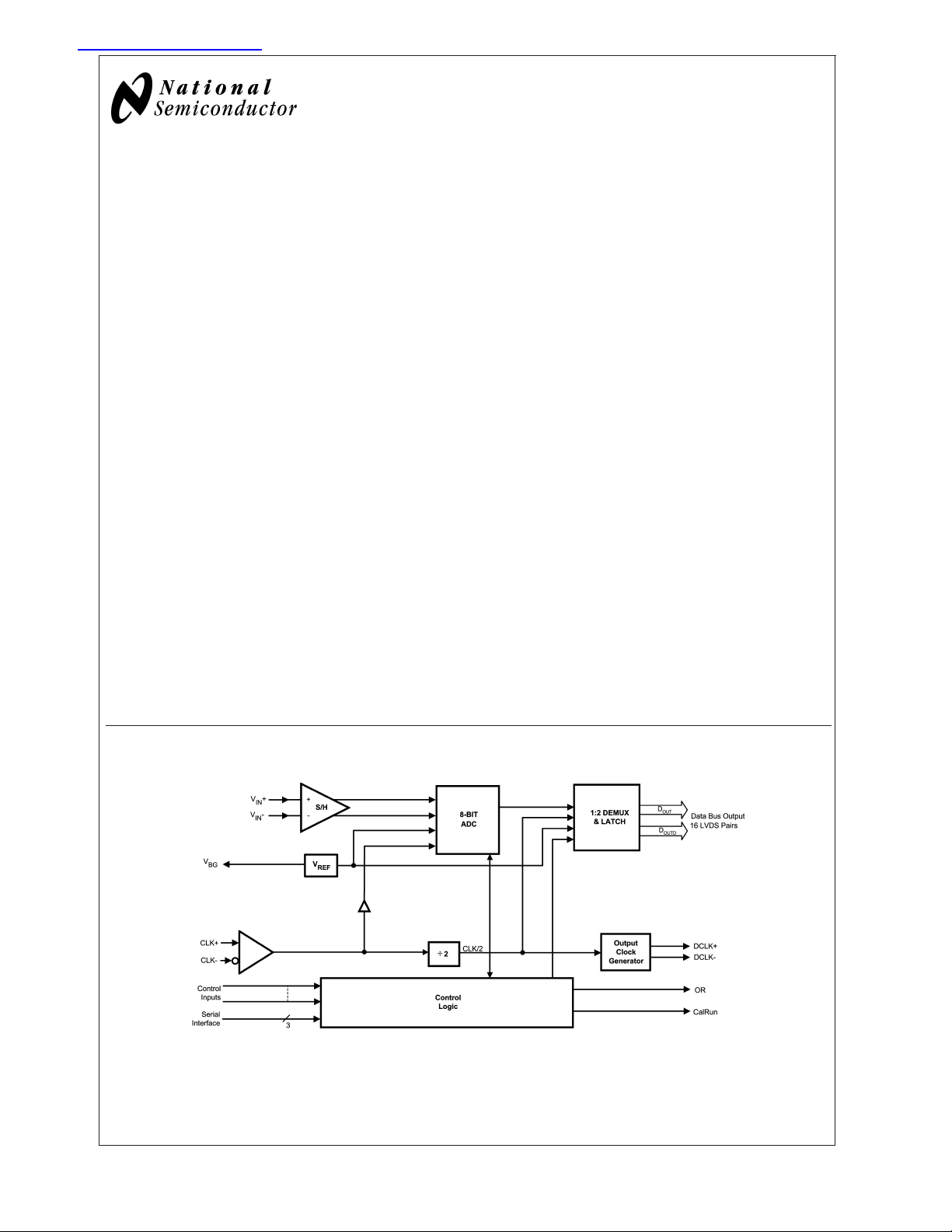
The ADC081500 is a low power, high performance CMOS
analog-to-digital converter that digitizes signals to 8 bits
resolution at sample rates up to 1.7 GSPS. Consuming a
typical 1.2 W at 1.5 GSPS from a single 1.9 Volt supply, this
device is guaranteed to have no missing codes over the full
operating temperature range. The unique folding and interpolating architecture, the fully differential comparator design,
the innovative design of the internal sample-and-hold amplifier and the self-calibration scheme enable a very flat response of all dynamic parameters beyond Nyquist, producing a high 7.3 ENOB with a 748 MHz input signal and a 1.5
GHz sample rate while providing a 10
formatting is offset binary and the LVDS digital outputs are
compliant with IEEE 1596.3-1996, with the exception of an
adjustable common mode voltage between 0.8V and 1.2V.
The converter output has a 1:2 demultiplexer that feeds two
LVDS buses and reduces the output data rate on each bus to
one-half the sample rate.
The converter typically consumes less than 3.5 mW in the
Power Down Mode and is available in a 128-lead, thermally
enhanced exposed pad LQFP and operates over the Industrial (-40˚C ≤ T
≤ +85˚C) temperature range.
A
-18
B.E.R. Output
Features
n Internal Sample-and-Hold
n Single +1.9V
n Choice of SDR or DDR output clocking
n Multiple ADC Synchronization Capability
n Guaranteed No Missing Codes
n Serial Interface for Extended Control
n Fine Adjustment of Input Full-Scale Range and Offset
n Duty Cycle Corrected Sample Clock
±
0.1V Operation
Key Specifications
n Resolution 8 Bits
n Max Conversion Rate 1.5 GSPS (min)
n Bit Error Rate 10
n ENOB
n DNL
n Power Consumption
@
748 MHz Input 7.3 Bits (typ)
±
— Operating 1.2 W (typ)
— Power Down Mode 3.5 mW (typ)
-18
(typ)
0.15 LSB (typ)
Applications
n Direct RF Down Conversion
n Digital Oscilloscopes
n Satellite Set-top boxes
n Communications Systems
n Test Instrumentation
Block Diagram
20153153
© 2005 National Semiconductor Corporation DS201531 www.national.com
Ordering Information
ADC081500
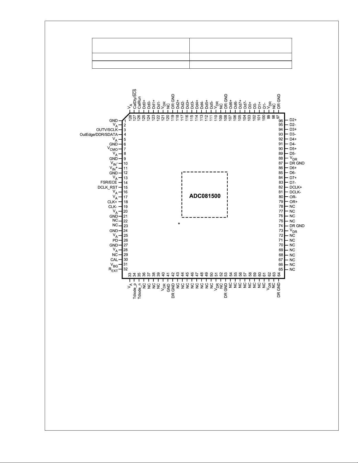
Pin Configuration
Industrial Temperature Range
<
<
T
(-40˚C
ADC081500CIYB 128-Pin Exposed Pad LQFP
ADC081500EVAL Evaluation Board
A
+85˚C)
NS Package
* Exposed pad on back of package must be soldered to ground plane to ensure rated performance.
www.national.com 2
20153101
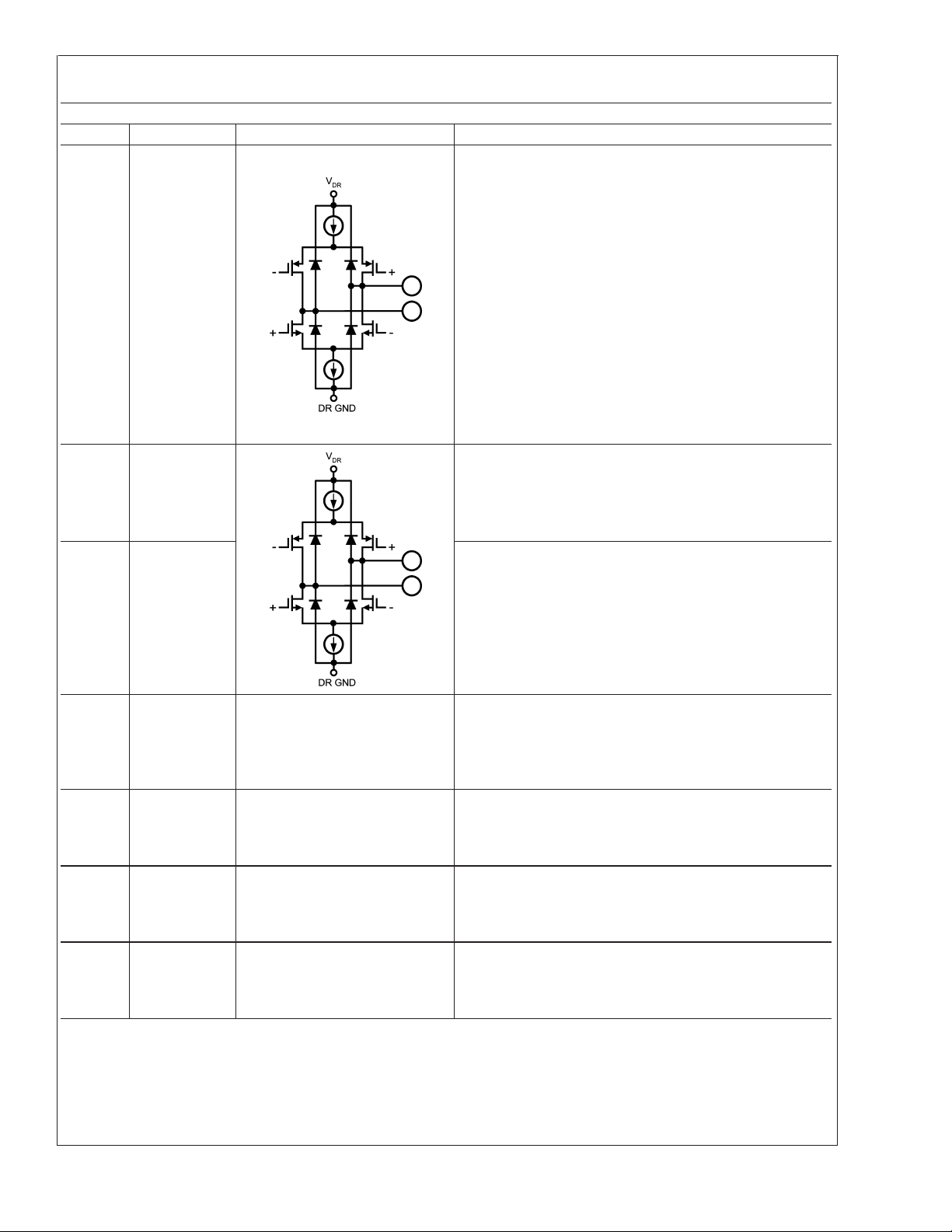
Pin Descriptions and Equivalent Circuits
Pin Functions
Pin No. Symbol Equivalent Circuit Description
Output Voltage Amplitude and Serial Interface Clock. Tie this
pin high for normal differential DCLK and data amplitude.
3 OutV / SCLK
OutEdge / DDR
4
/ SDATA
15 DCLK_RST
26 PD
30 CAL
14 FSR/ECE
127 CalDly / SCS
Ground this pin for a reduced differential output amplitude and
reduced power consumption. See Section 1.1.6. When the
extended control mode is enabled, this pin functions as the
SCLK input which clocks in the serial data. See Section 1.3
DCLK Edge Select, Double Data Rate Enable and Serial Data
Input. This input sets the output edge of DCLK+ at which the
output data transitions. (See Section 1.1.5.2). When this pin is
floating or connected to 1/2 the supply voltage, DDR clocking
is enabled. When the extended control mode is enabled, this
pin functions as the (SDATA) input. See Section 1.2 for
details on the extended control mode.
DCLK Reset. A positive pulse on this pin is used to reset and
synchronize the DCLK outputs of multiple converters. See
Section 1.5 for detailed description.
Power Down Pin. A logic high on the PD pin puts the device
into the Power Down Mode.
Calibration Cycle Initiate. A minimum 80 input clock cycles
logic low followed by a minimum of 80 input clock cycles high
on this pin initiates the self calibration sequence. See Section
2.4.2.
Full Scale Range Select and Extended Control Enable. In
non-extended control mode, a logic low on this pin sets the
full-scale differential input range to 650 mV
this pin sets the full-scale differential input range to 870
. See Section 1.1.4. To enable the extended control
mV
P-P
mode, whereby the serial interface and control registers are
employed, allow this pin to float or connect it to a voltage
equal to V
/2. See Section 1.2 for information on the
A
extended control mode.
Calibration Delay and Serial Interface Chip Select. With a
logic high or low on pin 14, this pin functions as Calibration
Delay and sets the number of input clock cycles after power
up before calibration begins (See Section 1.1.1). With pin 14
floating, this pin acts as the enable pin for the serial interface
input and the CalDly value becomes "0" (short delay with no
provision for a long power-up calibration delay).
. A logic high on
P-P
ADC081500
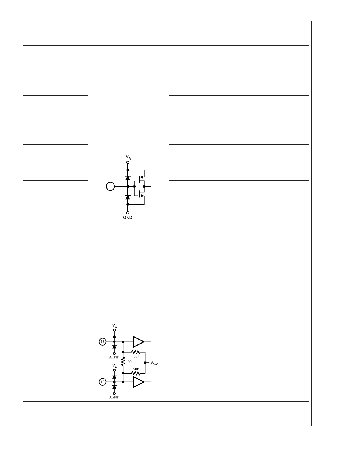
18
19
CLK+
CLK-
LVDS Clock input pins for the ADC. The differential clock
signal must be a.c. coupled to these pins. The input signal is
sampled on the falling edge of CLK+. See Section 2.3.
www.national.com3
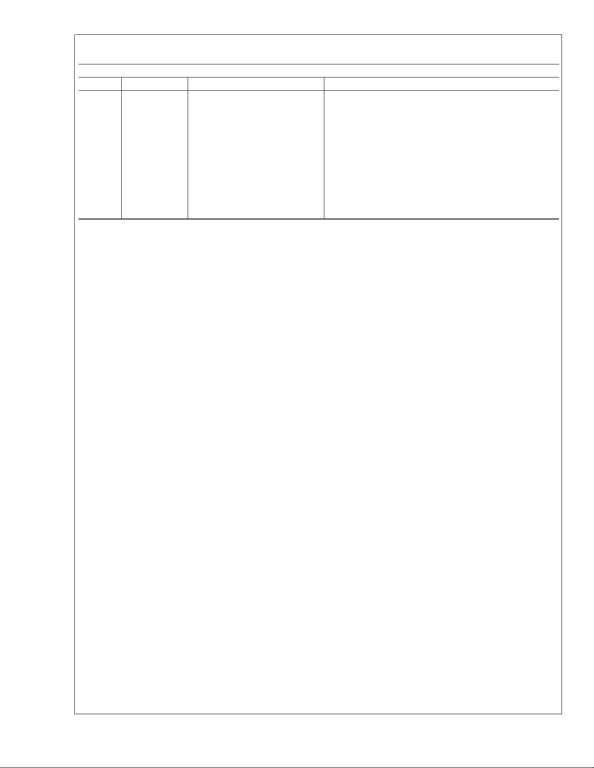
Pin Descriptions and Equivalent Circuits (Continued)
Pin Functions
Pin No. Symbol Equivalent Circuit Description
ADC081500
11
10
7V
31 V
V
V
IN
IN
CMO
BG
+
−
126 CalRun
32 R
EXT
Analog signal inputs to the ADC. The differential full-scale
input range is 650 mV
when the FSR pin is high.
mV
P-P
when the FSR pin is low, or 870
P-P
Common Mode Voltage. The voltage output at this pin is
required to be the common mode input voltage at V
− when d.c. coupling is used. This pin should be grounded
V
IN
+ and
IN
when a.c. coupling is used at the analog inputs. This pin is
capable of sourcing or sinking 100µA. See Section 2.2.
Bandgap output voltage capable of 100 µA source/sink.
Calibration Running indication. This pin is at a logic high when
calibration is running.
External bias resistor connection. Nominal value is 3.3k-Ohms
±
0.1%) to ground. See Section 1.1.1.
(
34
35
83
84
85
86
89
90
91
92
93
94
95
96
100
101
102
103
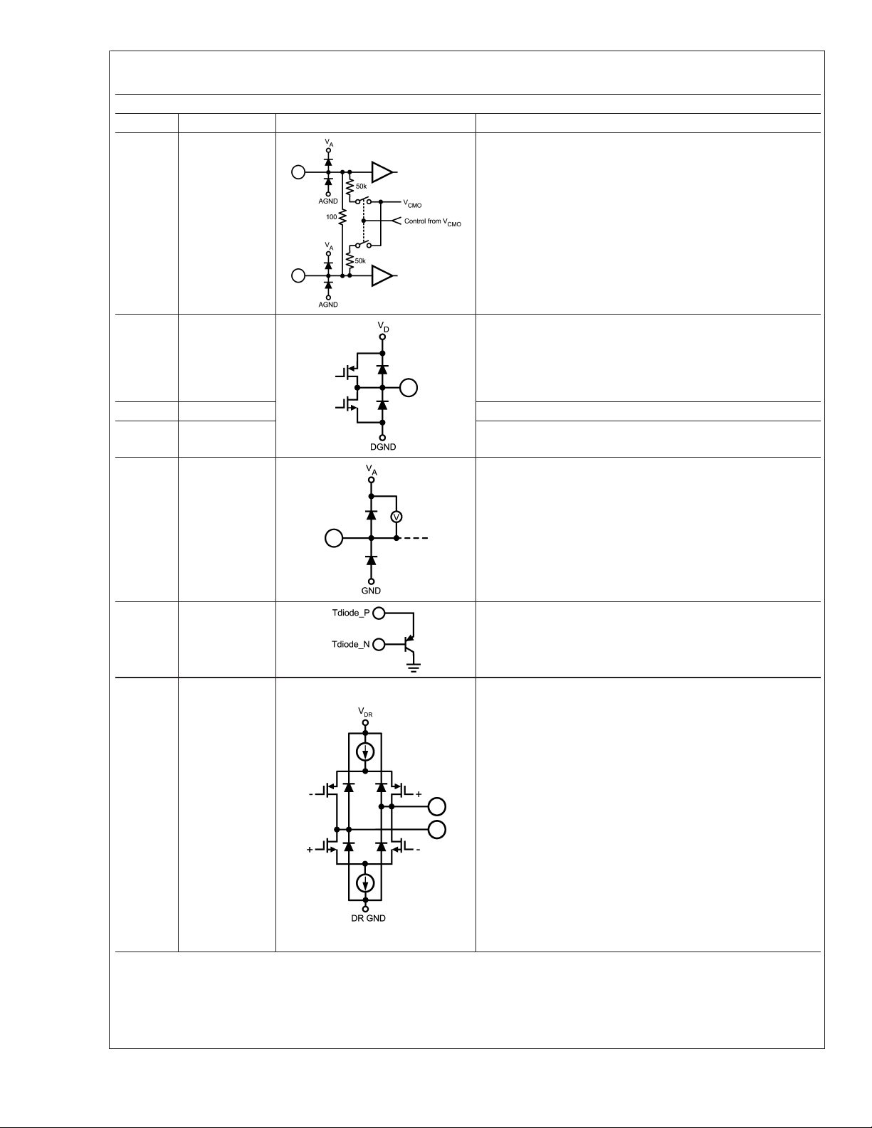
Tdiode_P
Tdiode_N
D7−
D7+
D6−
D6+
D5−
D5+
D4−
D4+
D3−
D3+
D2−
D2+
D1−
D1+
D0−
D0+
Temperature Diode Positive (Anode) and Negative (Cathode)
for die temperature measurements. See Section 2.6.2.
The LVDS Data Outputs that are not delayed in the output
demultiplexer. Compared with the Dd outputs, these outputs
represent the later time samples. These outputs should
always be terminated with a 100Ω differential resistor.
www.national.com 4
Pin Descriptions and Equivalent Circuits (Continued)
Pin Functions
Pin No. Symbol Equivalent Circuit Description
104
105
106
107
111
112
113
114
115
116
117
118
122
123
124
125
Dd7−
Dd7+
Dd6−
Dd6+
Dd5−
Dd5+
Dd4−
Dd4+
Dd3−
Dd3+
Dd2−
Dd2+
Dd1−
Dd1+
Dd0
Dd0
The LVDS Data Outputs that are delayed by one CLK cycle in
the output demultiplexer. Compared with the D outputs, these
outputs represent the earlier time sample. These outputs
should always be terminated with a 100Ω differential resistor.
ADC081500
79
80
82
81
2, 5, 8,
13, 16,
17, 20,
25, 28,
33, 128
40, 51
,62, 73,
88, 99,
110, 121
1, 6, 9,
12, 21,
24, 27,
41
42, 53,
64, 74,
87, 97,
108, 119
OR+
OR-
Out Of Range output. A differential high at these pins
indicates that the differential input is out of range (outside the
±
range
325 mV or±435 mV as defined by the FSR pin).
Differential Clock outputs used to latch the output data.
Delayed and non-delayed data outputs are supplied
DCLK+
DCLK-
synchronous to this signal. This signal is at 1/2 the input clock
rate in SDR mode and at 1/4 the input clock rate in the DDR
mode. The DCLK outputs are not active during a calibration
cycle.
V
A
V
DR
Analog power supply pins. Bypass these pins to ground.
Output Driver power supply pins. Bypass these pins to DR
GND.
GND Ground return for V
DR GND Ground return for V
.
A
.
DR
www.national.com5
Pin Descriptions and Equivalent Circuits (Continued)
Pin Functions
Pin No. Symbol Equivalent Circuit Description
ADC081500
22, 23,
29,
36-39,
43-50,
52,
54-61,
63,
65-72,
75-78,
98, 109,
120
NC No Connection. Make no connection to these pins.
www.national.com 6
ADC081500
Absolute Maximum Ratings
(Notes 1, 2)
If Military/Aerospace specified devices are required,
please contact the National Semiconductor Sales Office/
Distributors for availability and specifications.
Supply Voltage (V
Voltage on Any Input Pin −0.15V to (V
Ground Difference
|GND - DR GND| 0V to 100 mV
Input Current at Any Pin (Note 3)
Package Input Current (Note 3)
Power Dissipation at T
ESD Susceptibility (Note 4)
Human Body Model
Machine Model
Soldering Temperature, Infrared,
10 seconds, (Note 5), (Applies
to standard plated package only) 235˚C
Storage Temperature −65˚C to +150˚C
) 2.2V
A,VDR
≤ 85˚C 2.0 W
A
+0.15V)
±
25 mA
±
50 mA
2500V
250V
A
Operating Ratings (Notes 1, 2)
Ambient Temperature Range −40˚C ≤ T
Supply Voltage (V
Driver Supply Voltage (V
) +1.8V to +2.0V
A
) +1.8V to V
DR
Analog Input Common Mode
Voltage V
V
+, VIN- Voltage Range
IN
(Maintaining Common Mode) 200mV to V
Ground Difference
(|GND - DR GND|) 0V
CLK Pins Voltage Range 0V to V
Differential CLK Amplitude 0.4V
P-P
A
CMO
to 2.0V
≤ +85˚C
±
50mV
Package Thermal Resistance
Package θ
128-Lead
Exposed Pad
26˚C / W 10˚C / W 2.8˚C / W
θ
JA
JC (Top of
Package)
θ
J-PAD
(Thermal
Pad)
LQFP
Converter Electrical Characteristics
The following specifications apply after calibration for VA=VDR= +1.9VDC, OutV = 1.9V, VIN(a.c. coupled) Full Scale Range =
differential 870mV
cycle, V
= Floating, Normal Control Mode, Single Data Rate Mode, R
BG
= 100Ω Differential. Boldface limits apply for T
= 10 pF, Differential (a.c. coupled) sinewave input clock, f
P-P,CL
A=TMIN
to T
MAX
= 3300Ω±0.1%, Analog Signal Source Impedance
EXT
. All other limits TA= 25˚C, unless otherwise noted. (Notes 6,
7)
Symbol Parameter Conditions
STATIC CONVERTER CHARACTERISTICS
INL Integral Non-Linearity (Best fit)
DNL Differential Non-Linearity
DC Coupled, 1MHz Sine Wave
Overanged
DC Coupled, 1MHz Sine Wave
Overanged
Resolution with No Missing
Codes
V
OFF
V
_ADJ Input Offset Adjustment Range Extended Control Mode
OFF
Offset Error -0.45
PFSE Positive Full-Scale Error (Note 9) −0.6
NFSE Negative Full-Scale Error (Note 9) −1.31
FS_ADJ Full-Scale Adjustment Range Extended Control Mode
DYNAMIC CONVERTER CHARACTERISTICS
FPBW Full Power Bandwidth 1.7 GHz
B.E.R. Bit Error Rate 10
Gain Flatness
ENOB Effective Number of Bits
SINAD
Signal-to-Noise Plus Distortion
Ratio
SNR Signal-to-Noise Ratio
d.c. to 500 MHz
d.c. to 1 GHz
f
= 373 MHz, VIN= FSR − 0.5 dB 7.4 7.0 Bits (min)
IN
f
= 748 MHz, VIN= FSR − 0.5 dB 7.3 Bits (min)
IN
f
= 373 MHz, VIN= FSR − 0.5 dB 46.3 43.9 dB (min)
IN
f
= 748 MHz, VIN= FSR − 0.5 dB 45.4 dB (min)
IN
f
= 373 MHz, VIN= FSR − 0.5 dB 47 44.5 dB (min)
IN
f
= 748 MHz, VIN= FSR − 0.5 dB 46.3 dB (min)
IN
= 1.5 GHz at 0.5V
CLK
Typical
(Note 8)
±
0.3
±
0.15
P-P
Limits
(Note 8)
±
0.9 LSB (max)
±
0.6 LSB (max)
8 Bits
−1.5
1.0
±
45 mV
±
25 mV (max)
±
25 mV (max)
±
20
-18
±
0.5 dBFS
±
1.0 dBFS
±
15 %FS
with 50% duty
Units
(Limits)
LSB (min)
LSB (max)
Error/Sample
A
A
A
P-P
www.national.com7
Converter Electrical Characteristics (Continued)
The following specifications apply after calibration for VA=VDR= +1.9VDC, OutV = 1.9V, VIN(a.c. coupled) Full Scale Range =
differential 870mV
ADC081500
cycle, V
= Floating, Normal Control Mode, Single Data Rate Mode, R
BG
= 100Ω Differential. Boldface limits apply for T
= 10 pF, Differential (a.c. coupled) sinewave input clock, f
P-P,CL
A=TMIN
7)
Symbol Parameter Conditions
DYNAMIC CONVERTER CHARACTERISTICS
= 373 MHz, VIN= FSR − 0.5 dB -54.5 -47 dB (max)
f
THD Total Harmonic Distortion
2nd Harm Second Harmonic Distortion
3rd Harm Third Harmonic Distortion
SFDR Spurious-Free dynamic Range
IMD Intermodulation Distortion
Out of Range Output Code
(In addition to OR Output high)
IN
f
= 748 MHz, VIN= FSR − 0.5 dB -53 dB (max)
IN
f
= 373 MHz, VIN= FSR − 0.5 dB −60 dB
IN
f
= 748 MHz, VIN= FSR − 0.5 dB -57 dB
IN
f
= 373 MHz, VIN= FSR − 0.5 dB −62 dB
IN
f
= 748 MHz, VIN= FSR − 0.5 dB -65 dB
IN
f
= 373 MHz, VIN= FSR − 0.5 dB 56 48.5 dB (min)
IN
f
= 748 MHz, VIN= FSR − 0.5 dB 53 dB (min)
IN
f
= 321 MHz, VIN=FSR−7dB
IN1
= 326 MHz, VIN=FSR−7dB
f
IN2
(V
+)−(VIN−)>+ Full Scale 255
IN
(V
+)−(VIN−)<− Full Scale 0
IN
ANALOG INPUT AND REFERENCE CHARACTERISTICS
V
IN
V
CMI
C
IN
R
IN
Full Scale Analog Differential
Input Range
Analog Input Common Mode
Voltage
Analog Input Capacitance
(Notes 10, 11)
Differential Input Resistance 100
FSR pin 14 Low 650
FSR pin 14 High 870
Differential 0.02 pF
Each input pin to ground 1.6 pF
ANALOG OUTPUT CHARACTERISTICS
V
CMO
TC V
V
CMO_LVL
C
LOAD
V
CMO
V
BG
TC V
C
LOAD
V
BG
CMO
BG
Common Mode Output Voltage 1.26
Common Mode Output Voltage
Temperature Coefficient
V
input threshold to set DC
CMO
Coupling mode
Maximum V
CMO
load
= −40˚C to +85˚C 118 ppm/˚C
T
A
= 1.8V 0.60 V
V
A
V
= 2.0V 0.66 V
A
Capacitance
Bandgap Reference Output
Voltage
Bandgap Reference Voltage
Temperature Coefficient
=±100 µA 1.26
I
BG
TA= −40˚C to +85˚C,
=±100 µA
I
BG
Maximum Bandgap Reference
load Capacitance
TEMPERATURE DIODE CHARACTERISTICS
192 µA vs. 12 µA,
= 25˚C
T
∆V
BE
Temperature Diode Voltage
J
192 µA vs. 12 µA,
= 85˚C
T
J
to T
= 3300Ω±0.1%, Analog Signal Source Impedance
EXT
. All other limits TA= 25˚C, unless otherwise noted. (Notes 6,
MAX
= 1.5 GHz at 0.5V
CLK
Typical
(Note 8)
P-P
Limits
(Note 8)
-50 dB
570 mV
730 mV
790 mV
950 mV
V
−50
V
CMO
CMO
+50
V
CMO
94 Ω (min)
106 Ω (max)
0.95
1.45
80 pF
1.20
1.33
28 ppm/˚C
80 pF
71.23 mV
85.54 mV
with 50% duty
Units
(Limits)
(min)
P-P
(max)
P-P
(min)
P-P
(max)
P-P
mV (min)
mV (max)
V (min)
V (max)
V (min)
V (max)
www.national.com 8
Converter Electrical Characteristics (Continued)
The following specifications apply after calibration for VA=VDR= +1.9VDC, OutV = 1.9V, VIN(a.c. coupled) Full Scale Range =
differential 870mV
cycle, V
= Floating, Normal Control Mode, Single Data Rate Mode, R
BG
= 100Ω Differential. Boldface limits apply for T
= 10 pF, Differential (a.c. coupled) sinewave input clock, f
P-P,CL
A=TMIN
to T
MAX
7)
Symbol Parameter Conditions
CLOCK INPUT CHARACTERISTICS
Sine Wave Clock 0.6
V
ID
Differential Clock Input Level
Square Wave Clock 0.6
I
I
C
IN
Input Current VIN=0orVIN=V
Input Capacitance
(Notes 10, 11)
Differential 0.02 pF
Each input to ground 1.5 pF
A
DIGITAL CONTROL PIN CHARACTERISTICS
V
IH
V
IL
C
IN
Logic High Input Voltage (Note 12) 0.85 x V
Logic Low Input Voltage (Note 12) 0.15 x V
Input Capacitance
(Notes 11, 13)
Each input to ground 1.2 pF
DIGITAL OUTPUT CHARACTERISTICS
Measured differentially, OutV = V
= Floating (Note 15)
V
∆ V
V
V
∆ V
I
OS
Z
O
V
V
OD
OS
OS
OH
OL
O DIFF
OS
LVDS Differential Output
Voltage
Change in LVDS Output Swing
Between Logic Levels
Output Offset Voltage VBG= Floating 800 mV
Output Offset Voltage VBG=VA(Note 15) 1200 mV
Output Offset Voltage Change
Between Logic Levels
Output Short Circuit Current
Differential Output Impedance 100 Ohms
CalRun H level output IOH= -400uA (Note 12) 1.65 1.5 V
CalRun L level output IOH= 400uA (Note 12) 0.15 0.3 V
V
BG
Measured differentially, OutV =
GND, V
= Floating (Note 15)
BG
Output+ & Output- connected to
0.8V
POWER SUPPLY CHARACTERISTICS
I
A
I
DR
P
D
PSRR1
PSRR2
Analog Supply Current
Output Driver Supply Current
Power Consumption
D.C. Power Supply Rejection
Ratio
A.C. Power Supply Rejection
Ratio
PD = Low
PD = High
PD = Low
PD = High
PD = Low
PD = High
Change in Full Scale Error with
change in V
248 MHz, 50mV
from 1.8V to 2.0V
A
P-P
AC ELECTRICAL CHARACTERISTICS
f
f
CLK1
CLK2
Maximum Input Clock
Frequency
Minimum Input Clock
Frequency
= 3300Ω±0.1%, Analog Signal Source Impedance
EXT
. All other limits TA= 25˚C, unless otherwise noted. (Notes 6,
riding on V
A
= 1.5 GHz at 0.5V
CLK
Typical
(Note 8)
,
A
with 50% duty
P-P
Limits
(Note 8)
0.4
2.0
0.4
2.0
±
1µA
A
A
710
510
±
1mV
±
1mV
±
4mA
524
400 mV
920 mV
280 mV
720 mV
600 mA (max)
1.8
116
165 mA (max)
0.012
1.2
1.45 W (max)
3.5
Units
(Limits)
V
P-P
V
P-P
V
P-P
V
P-P
V (min)
V (max)
P-P
P-P
P-P
P-P
mA
mA
mW
(min)
(max)
(min)
(max)
(min)
(max)
(min)
(max)
30 dB
51 dB
1.7 1.5 GHz (min)
200 MHz
ADC081500
www.national.com9
 Loading...