

查询ADC08131供应商查询ADC08131供应商
ADC08131/ADC08134/ADC08138
8-Bit High-Speed Serial I/O A/D Converters with
Multiplexer Options, Voltage Reference, and Track/Hold
Function
June 1999
ADC08131/ADC08134/ADC08138 8-Bit High-Speed Serial I/O A/D Converters with Multiplexer
Options, Voltage Reference, and Track/Hold Function
General Description
The ADC08131/ADC08134/ADC08138 are 8-bit successive
approximation A/D converters with serial I/O and configurable input multiplexers with up to 8 channels. The serial
I/O is configuredto comply with the NSC MICROWIRE
rial data exchange standard for easy interface to the
™
COPS
family of controllers, and can easily interface with
standard shift registers or microprocessors.
All three devices provide a 2.5V band-gap derived reference
with guaranteed performance over temperature.
Atrack/hold function allows the analog voltage at the positive
input to vary during the actual A/D conversion.
The analog inputs can be configured to operate in various
combinations of single-ended, differential, or
pseudo-differential modes. In addition, input voltage spans
as small as 1V can be accommodated.
™
se-
Ordering Information
Industrial Package
(−40˚C ≤ T
ADC08131CIWM M14B
ADC08134CIWM M14B
ADC08138CIWM M20B
A
Applications
n Digitizing automotive sensors
n Process control/monitoring
n Remote sensing in noisy environments
n Embedded diagnostics
Features
n Serial digital data link requires few I/O pins
n Analog input track/hold function
n 4- or 8-channel input multiplexer options with address
logic
n On-chip 2.5V band-gap reference (
temperature guaranteed)
n No zero or full scale adjustment required
n TTL/CMOS input/output compatible
n 0V to 5V analog input range with single 5V power
supply
±
2%over
Key Specifications
n Resolution 8 Bits
n Conversion time (f
n Power dissipation 20 mW (Max)
n Single supply 5 V
n Total unadjusted error
n Linearity Error (V
n No missing codes (over temperature)
n On-board Reference +2.5V
≤ +85˚C)
=
1 MHz) 8 µs (Max)
C
1
±
⁄2LSB and±1 LSB
REF
=
2.5V)
(±5%)
DC
1
±
⁄2LSB
±
1.5%(Max)
TRI-STATE®is a registered trademark of National Semiconductor Corporation.
™
COPS
microcontrollers and MICROWIRE™are trademarks of National Semiconductor Corporation.
© 1999 National Semiconductor Corporation DS010749 www.national.com
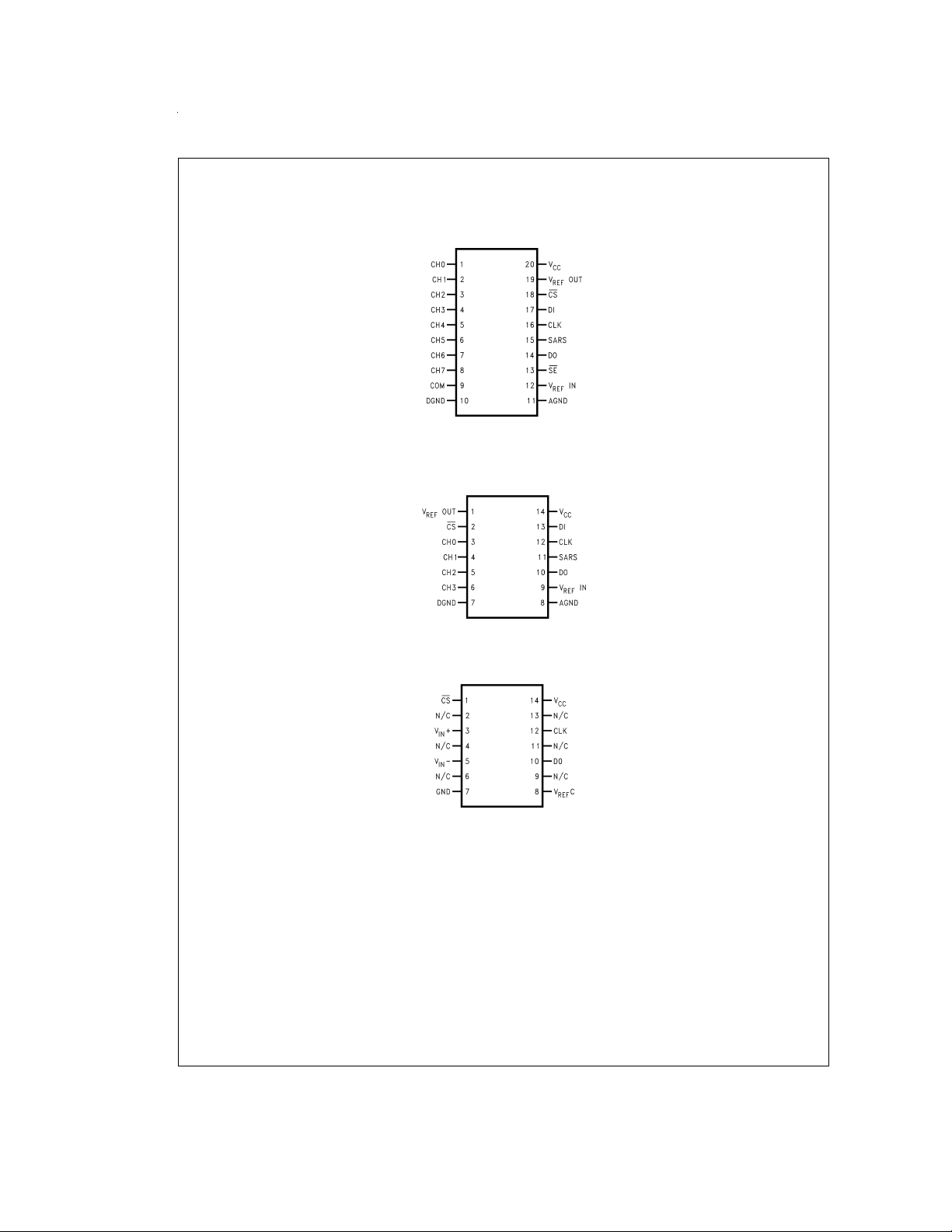
Connection Diagrams
ADC08138CIWM
Small Outline
Packages
DS010749-2
ADC08134CIWM
Small Outline
Packages
DS010749-3
ADC08131CIWM
Small Outline Package
www.national.com 2
DS010749-4
Absolute Maximum Ratings (Notes 1, 3)
If Military/Aerospace specified devices are required,
please contact the National Semiconductor Sales Office/
Distributors for availability and specifications.
Supply Voltage (V
Voltage at Inputs and Outputs −0.3V to V
Input Current at Any Pin (Note 4)
Package Input Current (Note 4)
Power Dissipation at T
(Note 5) 800 mW
ESD Susceptibility (Note 6) 1500V
) 6.5V
CC
CC
±
=
25˚C
A
+ 0.3V
±
5mA
20 mA
Soldering Information
N Package (10 sec.)
SO Package:
Vapor Phase (60 sec.)
Infrared (15 sec.) (Note 7)
260˚C
215˚C
220˚C
Storage Temperature −65˚C to +150˚C
Operating Ratings (Notes 2, 3)
Temperature Range T
Supply Voltage (V
) 4.5 VDCto 6.3 V
CC
≤ TA≤ T
MIN
MAX
−40˚C ≤ TA≤ +85˚C
DC
Electrical Characteristics
The following specifications apply for V
face limits apply for T
=
=
T
A
J
=
+5 V
CC
to T
T
MIN
DC,VREF
; all other limits T
MAX
Symbol Parameter Conditions
CONVERTER AND MULTIPLEXER CHARACTERISTICS
Linearity Error V
Full Scale Error V
Zero Error V
Total Unadjusted Error
Differential Linearity V
R
REF
V
IN
Reference Input Resistance (Note 11)
Analog Input Voltage (Note 12)
DC Common-Mode Error V
Power Supply Sensitivity
On Channel Leakage Current
(Note 13)
Off Channel Leakage Current
(Note 13)
DIGITAL AND DC CHARACTERISTICS
V
IN(1)
V
IN(0)
I
IN(1)
I
IN(0)
V
OUT(1)
V
OUT(0)
I
OUT
I
SOURCE
Logical “1” Input Voltage V
Logical “0” Input Voltage V
Logical “1” Input Current V
Logical “0” Input Current V
Logical “1” Output Voltage I
Logical “0” Output Voltage
TRI-STATE®Output Current
Output Source Current V
=
+2.5 V
=
+2.5 V
REF
=
+2.5 V
REF
=
+2.5 V
REF
=
+5 V
V
REF
(Note 10)
=
+2.5 V
REF
=
2.5 V
REF
=
V
+5V
CC
=
+2.5 V
V
REF
On Channel=5V, 0.2
Off Channel=0V 1
On Channel=0V, −0.2
Off Channel=5V −1
On Channel=5V, −0.2
Off Channel=0V −1
On Channel=0V, 0.2
Off Channel=5V 1
=
5.25V 2.0 V (min)
CC
=
4.75V 0.8 V (max)
CC
=
5.0V 1 µA (max)
IN
=
0V −1 µA (max)
IN
=
V
4.75V:
CC
=
−360 µA 2.4 V (min)
OUT
=
I
−10 µA 4.5 V (min)
OUT
=
V
4.75V 0.4 V (max)
CC
=
I
1.6 mA
OUT
=
V
0V −3.0 µA (max)
OUT
=
V
5V 3.0 µA (max)
OUT
=
0V −6.5 mA (min)
OUT
=
and f
DC
=
=
T
A
J
DC
DC
DC
DC
DC
1 MHz unless otherwise specified. Bold-
CLK
25˚C.
Typical
(Note 8)
Limits
(Note 9)
±
1 LSB (max)
±
1 LSB (max)
±
1 LSB (max)
±
1 LSB (max)
8 Bits (min)
Units
(Limits)
3.5 kΩ
1.3 kΩ (min)
6.0 kΩ (max)
(V
+ 0.05) V (max)
CC
(GND − 0.05) V (min)
1
±
⁄
DC
±
5%,
DC
2
1
±
⁄
4
LSB (max)
LSB (max)
µA (max)
µA (max)
µA (max)
µA (max)
www.national.com3
Electrical Characteristics (Continued)
The following specifications apply for V
face limits apply for T
=
=
T
A
J
=
+5 V
CC
to T
T
MIN
DC,VREF
; all other limits T
MAX
Symbol Parameter Conditions
DIGITAL AND DC CHARACTERISTICS
I
SINK
Output Sink Current V
Supply Current
I
CC
ADC08134, ADC08138 CS=HIGH 3.0 mA (max)
ADC08131 (Note 16) 6.0 mA (max)
OUT
=
+2.5 V
=
V
CC
=
and f
DC
=
=
T
A
J
1 MHz unless otherwise specified. Bold-
CLK
25˚C.
Typical
(Note 8)
Limits
(Note 9)
Units
(Limits)
8.0 mA (min)
Electrical Characteristics
The following specifications apply for V
=
=
to T
T
T
A
T
J
MIN
; all other limits T
MAX
=
, and f
+5 V
CC
DC
=
=
T
25˚C.
A
J
Symbol Parameter Conditions
REFERENCE CHARACTERISTICS
V
OUT Output Voltage DC08134, ADC08138
REF
/∆T Temperature Coefficient 40 ppm/˚C
∆V
REF
Sourcing
(0 ≤ I
ADC08134,
ADC08138
Sourcing
(0 ≤ I
/∆ILLoad Regulation (Note 17)
∆V
REF
ADC08131
Sinking
(−1 ≤ I
ADC08134,
ADC08138
Sinking
(−1 ≤ I
ADC08131
Line Regulation 4.75V ≤ V
V
REF
ADC08134, 8 25
I
SC
Short Circuit Current ADC08138
V
REF
ADC08131
V
T
∆V
SU
REF
Start-Up Time
/∆t Long Term Stability 200 ppm/1 kHr
CC
C
L
CLK
≤ +4 mA)
L
≤ +2 mA)
L
≤ 0 mA)
L
≤ 0 mA)
L
CC
=
0V
=
0V
:0V→5V
=
100 µF
=
1 MHz unless otherwise specified. Boldface limits apply for
Typical
(Note 8)
2.5
±
%
2
Limits
(Note 9)
±
2.5
1.5
%
0.003 0.1
0.003 0.1
0.2 0.5
0.2 0.5
≤ 5.25V 0.5 6 mV (max)
8 25
20 ms
Units
(Limits)
V
%
/mA
(max)
mA
(max)
Electrical Characteristics
The following specifications apply for V
limits apply for T
=
=
T
T
A
J
MIN
to T
MAX
CC
=
+5 V
DC,VREF
; all other limits T
Symbol Parameter Conditions
f
CLK
Clock Frequency
Clock Duty Cycle 40
(Note 14) 60
www.national.com 4
=
A
+2.5 V
=
T
J
=
DC
25˚C.
and t
=
=
t
20 ns unless otherwise specified. Boldface
r
f
Typical
(Note 8)
Limits
(Note 9)
10 kHz (min)
1 MHz (max)
Units
(Limits)
%
(min)
%
(max)
Electrical Characteristics (Continued)
The following specifications apply for V
limits apply for T
=
=
T
T
A
J
MIN
to T
MAX
CC
=
+5 V
DC,VREF
; all other limits T
Symbol Parameter Conditions
T
C
t
CA
t
SELECT
t
SET-UP
t
HOLD
t
pd1,tpd0
Conversion Time (Not Including
MUX Addressing Time) 8 µs (max)
Acquisition Time
CLK High while CS is High 50 ns
CS Falling Edge or Data Input
Valid to CLK Rising Edge
Data Input Valid after CLK Rising
Edge
CLK Falling Edge to Output Data
Valid (Note 15)
TRI-STATE Delay from Rising Edge
t
1H,t0H
C
IN
C
OUT
Note 1: Absolute Maximum Ratings indicate limits beyond which damage to the device may occur.
Note 2: Operating Ratings indicate conditions for which the device is functional. These ratings do not guarantee specific performance limits. For guaranteed speci-
fications and test conditions, see the Electrical Characteristics. The guaranteed specifications apply only for the test conditions listed. Some performance characteristics may degrade when the device is not operated under the listed test conditions.
Note 3: All voltages are measured with respect to AGND=DGND=0V
Note 4: When the input voltage (V
5 mA. The 20 mA maximum package input current rating limits the number of pins that can safely exceed the power supplies with an input current of 5 mA to four
pins.
Note 5: The maximum power dissipation must be derated at elevated temperatures and is dictated by T
allowable power dissipation at anytemperatureisP
T
JMAX
ADC08138.
Note 6: Human body model, 100 pF capacitor discharged through a 1.5 kΩ resistor.
Note 7: See AN450 “Surface Mounting Methods and Their Effect on Product Reliability” or Linear Data Book section “Surface Mount” for other methods of soldering
surface mount devices.
Note 8: Typicals are at T
Note 9: Guaranteed to National’s AOQL (Average Outgoing Quality Level).
Note 10: Total unadjusted error includes zero, full-scale, linearity, and multiplexer error. Total unadjusted error with V
ADC08138. See (Note 16).
Note 11: Cannot be tested for the ADC08131.
Note 12: For V
analog input voltages one diode drop below ground or one diode drop greater than V
(e.g., 5V) can cause an input diode to conduct, especially at elevated temperatures. This will cause errors for analog inputs near full-scale. The specification allows
50 mV forward bias of either diode; this means that as long as the analog V
Exceeding this range on an unselected channel will corrupt the reading of a selected channel. Achievement of an absolute 0 V
therefore require a minimum supply voltage of 4.950 V
Note 13: Channel leakage current is measured after a single-ended channel is selected and the clock is turned off. For off channel leakage current the following two
cases are considered: one, with the selected channel tied high (5 V
nels is measured; two, with the selected channel tied low and the off channels tied high, total current flow through the off channels is again measured. The two cases
considered for determining on channel leakage current are the same except total current flow through the selected channel is measured.
Note 14: A40%to 60%duty cycle range insures proper operation at all clock frequencies. In the case that an available clock has a duty cycle outside of these limits
the minimum time the clock is high or low must be at least 450 ns. The maximum time the clock can be high or low is 100 µs.
Note 15: Since data, MSB first, is the output of the comparator used in the successive approximation loop, an additional delay is built in (see Block Diagram) to allow
for comparator response time.
Note 16: For the ADC08131 V
reference current (700 µA typical, 2 mA maximum).
Note 17: Load regulation test conditions and specifications for the ADC08131 differ from those of the ADC08134 and ADC08138 because the ADC08131 has the
on-board reference as a permanent load.
of CS to Data Output and SARS
Hi-Z
Capacitance of Logic Inputs 5 pF
Capacitance of Logic Outputs 5 pF
) at any pin exceeds the power supplies (V
IN
=
(T
D
=
125˚C. The typical thermal resistances (θ
=
25˚C and represent the most likely parametric norm.
J
≥ V
IN(−)
the digital code will be 0000 0000. Two on-chip diodes are tied to each analog input (see Block Diagram) which will forward-conduct for
IN(+)
IN is internally tied to the on chip 2.5V band-gap reference output; therefore, the supply current is larger because it includes the
REF
JMAX−TA
) of these parts when board mounted for the ADC 08131 and the ADC08134 is 140˚C/W and 91˚C/W for the
JA
over temperature variations, initial tolerance and loading.
DC
=
+2.5 V
DC
=
=
T
A
J
=
1 MHz
f
CLK
25˚C.
and t
=
=
t
20 ns unless otherwise specified. Boldface
r
f
Typical
(Note 8)
Limits
(Note 9)
8 1/f
1
⁄
2
Units
(Limits)
CLK
1/f
CLK
25 ns (min)
20 ns (min)
=
C
100 pF:
L
Data MSB First 250 ns (max)
Data LSB First 200 ns (max)
=
C
10 pF, R
L
(see TRI-STATE Test Circuits)
=
100 pF, R
C
L
DC
)/θJAor the number given intheAbsoluteMaximumRatings,whicheveris lower. For these devices
IN
) and the remaining seven off channels tied low (0 VDC), total current flow through the off chan-
DC
=
10 kΩ
L
=
2kΩ 180 ns (max)
L
, unless otherwise specified.
<
(AGND or DGND) or V
IN
JMAX
supply.During testing at low VCClevels (e.g., 4.5V), high level analog inputs
CC
does not exceed the supply voltage by more than 50 mV, the output code will be correct.
50 ns
>
AVCC) the current at that pin should be limited to
IN
, θJAand the ambient temperature, TA. The maximum
=
+5V only applies to the ADC08134 and
REF
to5VDCinput voltage range will
DC
(max)
(max)
www.national.com5
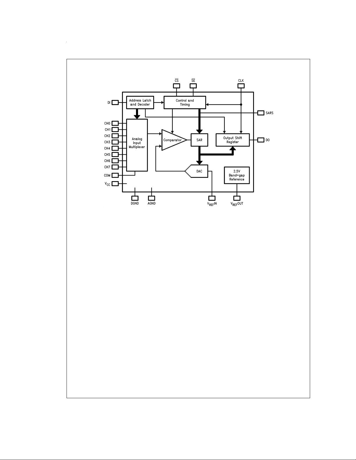
ADC08138 Simplified Block Diagram
DS010749-1
www.national.com 6
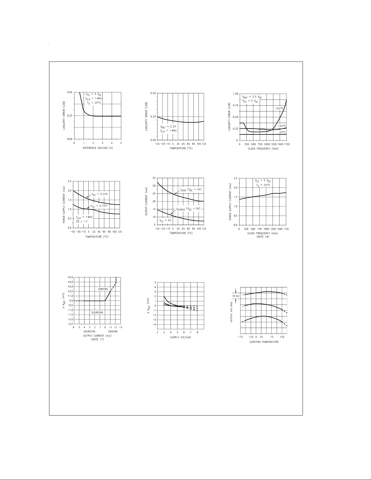
Typical Converter Performance Characteristics
Linearity Error vs
Reference Voltage
Power Supply Current vs
Temperature (ADC08138,
ADC08134)
Note: For ADC08131 add I
DS010749-27
DS010749-30
REF
Linearity Error vs
Temperature
Output Current vs
Temperature
DS010749-28
DS010749-31
Linearity Error vs
Clock Frequency
DS010749-29
Power Supply Current
vs Clock Frequency
DS010749-32
Typical Reference Performance Characteristics
Load Regulation
DS010749-33
Line Regulation
(3 Typical Parts)
DS010749-34
Output Drift
vs Temperature
(3 Typical Parts)
DS010749-35
www.national.com7
 Loading...