

查询ADC0800供应商查询ADC0800供应商
ADC0800 8-Bit A/D Converter
ADC0800 8-Bit A/D Converter
February 1995
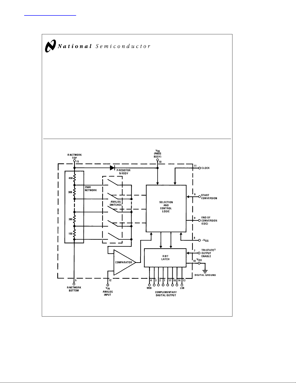
General Description
The ADC0800 is an 8-bit monolithic A/D converter using Pchannel ion-implanted MOS technology. It contains a high
input impedance comparator, 256 series resistors and analog switches, control logic and output latches. Conversion is
performed using a successive approximation technique
where the unknown analog voltage is compared to the resistor tie points using analog switches. When the appropriate tie point voltage matches the unknown voltage, conversion is complete and the digital outputs contain an 8-bit
complementary binary word corresponding to the unknown.
The binary output is TRI-STATE
to permit bussing on com-
É
mon data lines.
The ADC0800PD is specified over
the ADC0800PCD is specified over 0
b
55§Ctoa125§C and
Cto70§C.
§
Block Diagram
Features
Y
Low cost
Y
g
5V, 10V input ranges
Y
No missing codes
Y
Ratiometric conversion
Y
TRI-STATE outputs
Y
Fast T
Y
Contains output latches
Y
TTL compatible
Y
Supply voltages 5 VDCandb12 V
Y
Resolution 8 bits
Y
Linearity
Y
Conversion speed 40 clock periods
Y
Clock range 50 to 800 kHz
e
C
g
50 ms
DC
1 LSB
(00000000eafull-scale)
TRI-STATEÉis a registered trademark of National Semiconductor Corp.
C
1995 National Semiconductor Corporation RRD-B30M115/Printed in U. S. A.
TL/H/5670
TL/H/5670– 1

Absolute Maximum Ratings (Note 1)
If Military/Aerospace specified devices are required,
please contact the National Semiconductor Sales
Office/Distributors for availability and specifications.
Supply Voltage (V
)V
DD
Supply Voltage (VGG)V
a
Voltage at Any Input V
SS
0.3V to V
b
22V
SS
b
22V
SS
b
22V
SS
Input Current at Any Pin (Note 2) 5 mA
Package Input Current (Note 2) 20 mA
Power Dissipation (Note 3) 875 mW
ESD Susceptibility (Note 4) 500V
Storage Temperature 150
Lead Temperature (Soldering, 10 sec.) 300§C
Operating Ratings (Note 1)
s
s
T
Temperature Range T
ADC0800PD
b
55§CsT
ADC0800PCD 0
MIN
CsT
§
T
A
MAX
s
a
125§C
A
s
a
70§C
A
Electrical Characteristics
These specifications apply for V
on-chip R-network (V
kHz. For all tests, a 475X resistor is used from pin 5 to V
R-NETWORK TOP
e
SS
5.0 VDC,V
e
5.000 VDCand V
specifications apply over an ambient temperature range of
ADC0800PCD.
Parameter Conditions Min Typ Max Units
Non-Linearity T
Differential Non-Linearity
Zero Error
Zero Error Temperature Coefficient (Note 9) 0.01 %/§C
Full-Scale Error
Full-Scale Error Temperature Coefficient (Note 9) 0.01 %/§C
Input Leakage 1 mA
Logical ‘‘1’’ Input Voltage All Inputs V
Logical ‘‘0’’ Input Voltage All Inputs V
Logical Input Leakage T
Logical ‘‘1’’ Output Voltage All Outputs, I
Logical ‘‘0’’ Output Voltage All Outputs, I
Disabled Output Leakage T
Clock Frequency 0§CsT
Clock Pulse Duty Cycle 40 60 %
TRI-STATE Enable/Disable Time 1 ms
Start Conversion Pulse (Note 10) 1 3(/2 Clock
Power Supply Current T
Note 1: Absolute Maximum Ratings indicate limits beyond which damage to the device may occur. DC and AC electrical specifications do not apply when operating
the device beyond its specified operating conditions.
Note 2: When the input voltage (V
to 5 mA or less. The 20 mA package input current limits the number of pins that can exceed the power supply boundaries witha5mAcurrent limit to four.
Note 3: The maximum power dissipation must be derated at elevated temperatures and is dictated by T
allowable power dissipation at any temperature is P
device, T
Note 4: Human body model, 100 pF discharged through a 1.5 kX resistor.
Note 5: Typicals are at 25
Note 6: Tested limits are guaranteed to National’s AOQL (Average Outgoing Quality Level).
Note 7: Design limits are guaranteed but not 100% tested. These limits are not used to calculate outgoing quality levels.
Note 8: Non-linearity specifications are based on best straight line.
Note 9: Guaranteed by design only.
Note 10: Start conversion pulse duration greater than 3(/2 clock periods will cause conversion errors.
e
125§C, and the typical junction-to-ambient thermal resistance of the ADC0800PD and ADC0800PCD when board mounted is 66§C/W.
JMAX
) at any pin exceeds the power supply rails (V
IN
D
C and represent most likely parametric norm.
§
eb
12.0 VDC,V
GG
e
A
Over Temperature, (Note 8)
e
A
V
SS
e
A
V
SS
b
55§CsT
R-NETWORK BOTTOM
R-NETWORK BOTTOM
b
25§C, (Note 8)
25§C, All Inputs, V
b
10V
OH
e
OL
25§C, All Outputs, V
@
10V
s
a
70§C 50 800 kHz
A
s
a
A
e
0VDC, a reference voltage of 10.000 VDCacross the
DD
eb
5.000 VDC), and a clock frequency of 800
eb
5VDC. Unless otherwise noted, these
55§Ctoa125§C for the ADC0800PD and 0§Ctoa70§C for the
g
1 LSB
g
2 LSB
g
(/2 LSB
g
2 LSB
g
2 LSB
b
1.0 V
SS
GG
e
IL
e
100 mA 2.4 V
SS
b
V
4.2 V
SS
1 mA
1.6 mA 0.4 V
e
OL
2 mA
125§C 100 500 kHz
V
Periods
e
25§C20mA
A
k
IN
e
b
(T
TA)/iJAor the number given in the Absolute Maximum Ratings, whichever is lower. For this
JMAX
Vbor V
l
Va) the absolute value of current at that pin should be limited
IN
, iJA, and the ambient temperature, TA. The maximum
JMAX
C
§
2

Timing Diagram
Data is complementary binary (full scale is all ‘‘0’s’’ output).
Application Hints
OPERATION
The ADC0800 contains a network with 256-300X resistors
in series. Analog switch taps are made at the junction of
each resistor and at each end of the network. In operation,
a reference (10.00V) is applied across this network of 256
resistors. An analog input (V
ter point of the ladder via the appropriate switch. If V
larger than V
points and now compares V
/2, the internal logic changes the switch
REF
known as successive approximation, continues until the
best match of V
specific tap on the resistor network. When the conversion is
IN
and V
complete, the logic loads a binary word corresponding to
this tap into the output latch and an end of conversion
(EOC) logic level appears. The output latches hold this data
valid until a new conversion is completed and new data is
loaded into the latches. The data transfer occurs in about
200 ns so that valid data is present virtually all the time in
the latches. The data outputs are activated when the Output
Enable is high, and in TRI-STATE when Output Enable is
low. The Enable Delay time is approximately 200 ns. Each
conversion requires 40 clock periods. The device may be
operated in the free running mode by connecting the Start
Conversion line to the End of Conversion line. However, to
ensure start-up under all possible conditions, an external
Start Conversion pulse is required during power up conditions.
REFERENCE
The reference applied across the 256 resistor network determines the analog input range. V
of the R-network connected to 5V and the bottom connect-
b
ed to
5V gives ag5V range. The reference can be level
shifted between V
plied to the top of the R-network (pin 15), must not exceed
V
, to prevent forward biasing the on-chip parasitic silicon
SS
diodes that exist between the P-diffused resistors (pin 15)
SS
and the N-type body (pin 10, V
power supply for V
voltage tolerance and changes over temperature. A solution
is to power the V
of the op amp that is used to bias the top of the
SS
line (15 mA max drain) from the output
SS
) is first compared to the cen-
IN
and */4 V
IN
/N is made. N now defines a
REF
REF
. This process,
REF
e
10.00V with the top
IN
and VGG. However, the voltage, ap-
). Use of a standard logic
can cause problems, both due to initial
SS
R-network (pin 15). The analog input voltage and the voltage that is applied to the bottom of the R-network (pin 5)
must be at least 7V above the
b
VGGsupply voltage to
ensure adequate voltage drive to the analog switches.
Other reference voltages may be used (such as 10.24V). If a
5V reference is used, the analog range will be 5V and accuracy will be reduced by a factor of 2. Thus, for maximum
is
accuracy, it is desirable to operate with at least a 10V reference. For TTL logic levels, this requires 5V and
R-network. CMOS can operate at the 10 V
a single 10 V
levels for both inputs and outputs will be from ground to
V
.
SS
reference can be used. All digital voltage
DC
ANALOG INPUT AND SOURCE RESISTANCE
CONSIDERATIONS
The lead to the analog input (pin 12) should be kept as short
as possible. Both noise and digital clock coupling to this
input can cause conversion errors. To minimize any input
errors, the following source resistance considerations
should be noted:
s
For R
5k No analog input bypass capacitor re-
S
quired, although a 0.1 mF input bypass
capacitor will prevent pickup due to unavoidable series lead inductance.
s
k
For 5k
R
20k A 0.1 mF capacitor from the input (pin
S
l
For R
20k Input buffering is necessary.
S
12) to ground should be used.
If the overall converter system requires lowpass filtering of
the analog input signal, use a 20 kX or less series resistor
for a passive RC section or add an op amp RC active lowpass filter (with its inherent low output resistance) to ensure
accurate conversions.
CLOCK COUPLING
The clock lead should be kept away from the analog input
line to reduce coupling.
LOGIC INPUTS
The logical ‘‘1’’ input voltage swing for the Clock, Start Conversion and Output Enable should be (V
DCVSS
b
SS
b
1.0V).
TL/H/5670– 2
5V for the
level and
3

Application Hints (Continued)
CMOS will satisfy this requirement but a pull-up resistor
should be used for TTL logic inputs.
RE-START AND DATA VALID AFTER EOC
The EOC line (pin 9) will be in the low state for a maximum
of 40 clock periods to indicate ‘‘busy’’. A START pulse that
occurs while the A/D is BUSY will reset the SAR and start a
new conversion with the EOC signal remaining in the low
state until the end of this new conversion. When the conversion is complete, the EOC line will go to the high voltage
state. An additional 4 clock periods must be allowed to
elapse after EOC goes high, before a new conversion cycle
is requested. Start Conversion pulses that occur during this
last 4 clock period interval may be ignored (see
2
for high speed operation). This is a problem only for high
conversion rates and keeping the number of conversions
per second less than f
proper operation. For example, for an 800 kHz clock, ap-
/44 automatically guarantees
CLOCK
proximately 18,000 conversions per second are allowed.
The transfer of the new digital data to the output is initiated
when EOC goes to the high voltage state.
POWER SUPPLIES
Standard supplies are V
e
V
0V. Device accuracy is dependent on stability of the
DD
reference voltage and has slight sensitivity to V
V
has no effect on accuracy. Noise spikes on the V
DD
and VGGsupplies can cause improper conversion; there-
ea
5V, V
SS
fore, filtering each supply with a 4.7 mF tantalum capacitor is
recommended.
GG
Figure 1
eb
and
12V and
SSÐVGG
CONTINUOUS CONVERSIONS AND LOGIC CONTROL
Simply tying the EOC output to the Start Conversion input
will allow continuous conversions, but an oscillation on this
line will exist during the first 4 clock periods after EOC goes
high. Adding a D flip-flop between EOC (D input) to Start
Conversion (Q output) will prevent the oscillation and will
allow a stop/continuous control via the ‘‘clear’’ input.
To prevent missing a start pulse that may occur after EOC
goes high and prior to the required 4 clock period time interval, the circuit of
Figure 1
can be used. The RS latch can be
set at any time and the 4-stage shift register delays the
application of the start pulse to the A/D by 4 clock periods.
The RS latch is reset 1 clock period after the A/D EOC
signal goes to the low voltage state. This circuit also provides a Start Conversion pulse to the A/D which is 1 clock
period wide.
A second control logic application circuit is shown in
2
. This allows an asynchronous start pulse of arbitrary
length less than T
level and provides a single clock period start pulse to the
, to continuously convert for a fixed high
C
Figure
A/D. The binary counter is loaded with a count of 11 when
the start pulse to the A/D appears. Counting is inhibited
until the EOC signal from the A/D goes high. A carry pulse
is then generated 4 clock periods after EOC goes high and
.
SS
is used to reset the input RS latch. This carry pulse can be
used to indicate that the conversion is complete, the data
has transferred to the output buffers and the system is
ready for a new conversion cycle.
FIGURE 1. Delaying an Asynchronous Start Pulse
FIGURE 2. A/D Control Logic
4
TL/H/5670– 3
TL/H/5670– 10

Application Hints (Continued)
ZERO AND FULL-SCALE ADJUSTMENT
Zero Adjustment: This is the offset voltage required at the
bottom of the R-network (pin 5) to make the 11111111 to
11111110 transition when the input voltage is (/2 LSB (20
mV for a 10.24V scale). In most cases, this can be accomplished by havinga1kXpot on pin 5. A resistor of 475X
can be used as a non-adjustable best approximation from
pin 5 to ground.
Typical Applications
Full-Scale Adjustment: This is the offset voltage required
at the top of the R-network (pin 15) to make the 00000001
to 00000000 transition when the input voltage is 1 (/2 LSB
from full-scale (60 mV less than full-scale for a 10.24V
scale). This voltage is guaranteed to be within
g
2 LSB for
the ADC0800 without adjustment. In most cases, adjustment can be accomplished by having a 1 kX pot on pin 15.
General Connection
Hi-Voltage CMOS Output Levels
Ratiometric Input Signal with Tracking Reference
TL/H/5670– 11
TL/H/5670– 4
0V to 10V VINrange
0V to 10V output levels
TL/H/5670– 12
5
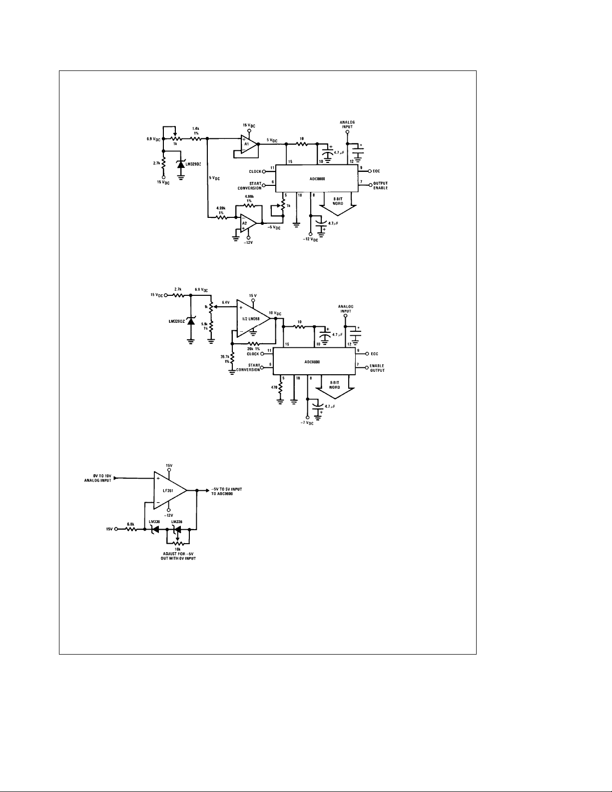
Typical Applications (Continued)
V
e
10 VDCWith TTL Logic Levels
REF
*See application hints
A1 and A2eLM358N dual op amp
e
V
REF
10 VDCWith 10V CMOS Logic Levels
Input Level Shifting
Permits TTL compatible outputs with
#
0V to 10V input range (0V to
input range achieved by reversing
polarity of zener diodes and returning
the 6.8k resistor to V
*See application hints
b
b
).
TL/H/5670– 13
TL/H/5670– 14
10V
TL/H/5670– 5
6

Typical Applications (Continued)
TESTING THE A/D CONVERTER
There are many degrees of complexity associated with testing an A/D converter. One of the simplest tests is to apply a
known analog input voltage to the converter and use LEDs
to display the resulting digital output code as shown in
ure 3
. Note that the LED drivers invert the digital output of
the A/D converter to provide a binary display. A lab DVM
can be used if a precision voltage source is not available.
After adjusting the zero and full-scale, any number of points
can be checked, as desired.
For ease of testing, a 10.24 V
for the A/D converter. This provides an LSB of 40 mV
reference is recommended
DC
(10.240/256). To adjust the zero of the A/D, an analog input
voltage of (/2 LSB or 20 mV should be applied and the
Fig-
zero adjust potentiometer should be set to provide a flicker
on the LSB LED readout with all the other display LEDs
OFF.
To adjust the full-scale adjust potentiometer, an analog input that is 1(/2 LSB less than the reference (10.240–0.060
or 10.180 V
the full-scale adjusted for a flicker on the LSB LED, but this
) should be applied to the analog input and
DC
time with all the other LEDs ON.
A complete circuit for a simple A/D tester is shown in
4
. Note that the clock input voltage swing and the digital
Figure
output voltage swings are from 0V to 10.24V. The
MM74C901 provides a voltage translation to 5V operation
and also the logic inversion so the readout LEDs are in binary.
FIGURE 3. Basic A/D Tester
FIGURE 4. Complete Basic Tester Circuit
TL/H/5670– 15
TL/H/5670– 7
7

Typical Applications (Continued)
The digital output LED display can be decoded by dividing
the 8 bits into the 4 most significant bits and 4 least significant bits. Table I shows the fractional binary equivalent of
these two 8-bit groups. By adding the decoded voltages
which are obtained from the column: ‘‘Input Voltage Value
with a 10.240 V
value of the digital display can be determined. For example,
for an output LED display of ‘‘1011 0110’’ or ‘‘B6’’ (in hex)
the voltage values from the table are 7.04
’’ of both the MS and LS groups, the
REF
a
0.24 or
7.280 V
ues of a perfect A/D converter. The input voltage has to
change by
ty’’ of an A/D, to obtain an output digital code change. The
effects of this quantization error have to be accounted for in
the interpretation of the test results. A plot of this natural
error source is shown in
analog input voltage and the error voltage are normalized to
LSBs.
TABLE I. DECODING THE DIGITAL OUTPUT LEDs
FRACTIONAL BINARY VALUE FOR VALUE WITH
HEX BINARY 10.24 V
MS GROUP LS GROUP MS GROUP LS GROUP
F 1 1 1 1 15/16 15/256 9.600 0.600
E 1 1 1 0 7/8 7/128 8.960 0.560
D 1 1 0 1 13/16 13/256 8.320 0.520
C 1 1 0 0 3/4 3/64 7.680 0.480
B 1 0 1 1 11/16 11/256 7.040 0.440
A 1 0 1 0 5/8 5/128 6.400 0.400
9 1 0 0 1 9/16 9/256 5.760 0.360
8 1 0 0 0 1/2 1/32 5.120 0.320
7 0 1 1 1 7/16 7/256 4.480 0.280
6 0 1 1 0 3/8 3/128 3.840 0.240
5 0 1 0 1 5/16 5/256 3.200 0.200
4 0 1 0 0 1/4 1/64 2.560 0.160
3 0 0 1 1 3/16 3/256 1.920 0.120
2 0 0 1 0 1/8 1/128 1.280 0.080
1 0 0 0 1 1/16 1/256 0.640 0.040
00000 00
. These voltage values represent the center val-
DC
g
(/2 LSB (g20 mV), the ‘‘quantization uncertain-
Figure 5
where, for clarity, both the
INPUT VOLTAGE
REF
TL/H/5670– 8
FIGURE 5. Error Plot of a Perfect A/D Showing Effects of Quantization Error
8
Typical Applications (Continued)
A low speed ramp generator can also be used to sweep the
analog input voltage and the LED outputs will provide a binary counting sequence from zero to full-scale.
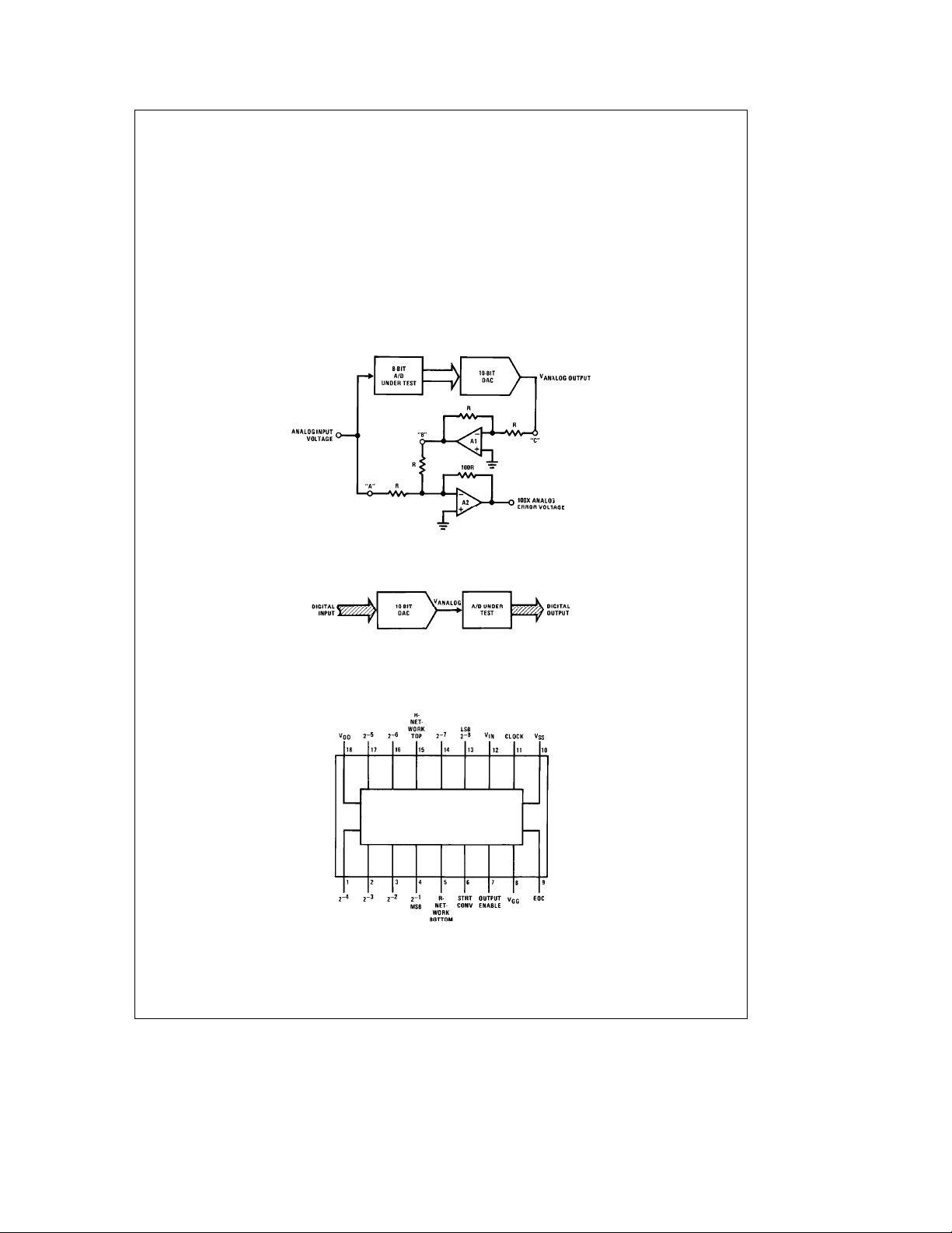
The techniques described so far are suitable for an engineering evaluation or a quick check on performance. For a
higher speed test system, or to obtain plotted data, a digitalto-analog converter is needed for the test set-up. An accurate 10-bit DAC can serve as the precision voltage source
for the A/D. Errors of the A/D under test can be provided as
either analog voltages or differences in two digital words.
A basic A/D tester which uses a DAC and provides the error
as an analog output voltage is shown in
amps can be eliminated if a lab DVM with a numerical subtraction feature is available to directly readout the difference
voltage, ‘‘A – C’’.
Figure 6
.The2op
For operation with a microprocessor or a computer-based
test system, it is more convenient to present the errors digitally. This can be done with the circuit of
output code transitions can be detected as the 10-bit DAC is
incremented. This provides (/4 LSB steps for the 8-bit A/D
under test. If the results of this test are automatically plotted
with the analog input on the X axis and the error (in LSB’s)
as the Y axis, a useful transfer function of the A/D under
test results. For acceptance testing, the plot is not necessary and the testing speed can be increased by establishing
internal limits on the allowed error for each code.
Figure 7
where the
Connection Diagram
All R’se0.05% tolerance
FIGURE 6. A/D Tester with Analog Error Output
FIGURE 7. Basic ‘‘Digital’’ A/D Tester
Dual-In-Line Package
Top View
Order Number ADC0800PD
or ADC0800PCD
See NS Package Number D18A
TL/H/5670– 16
TL/H/5670– 17
TL/H/5670– 9
9
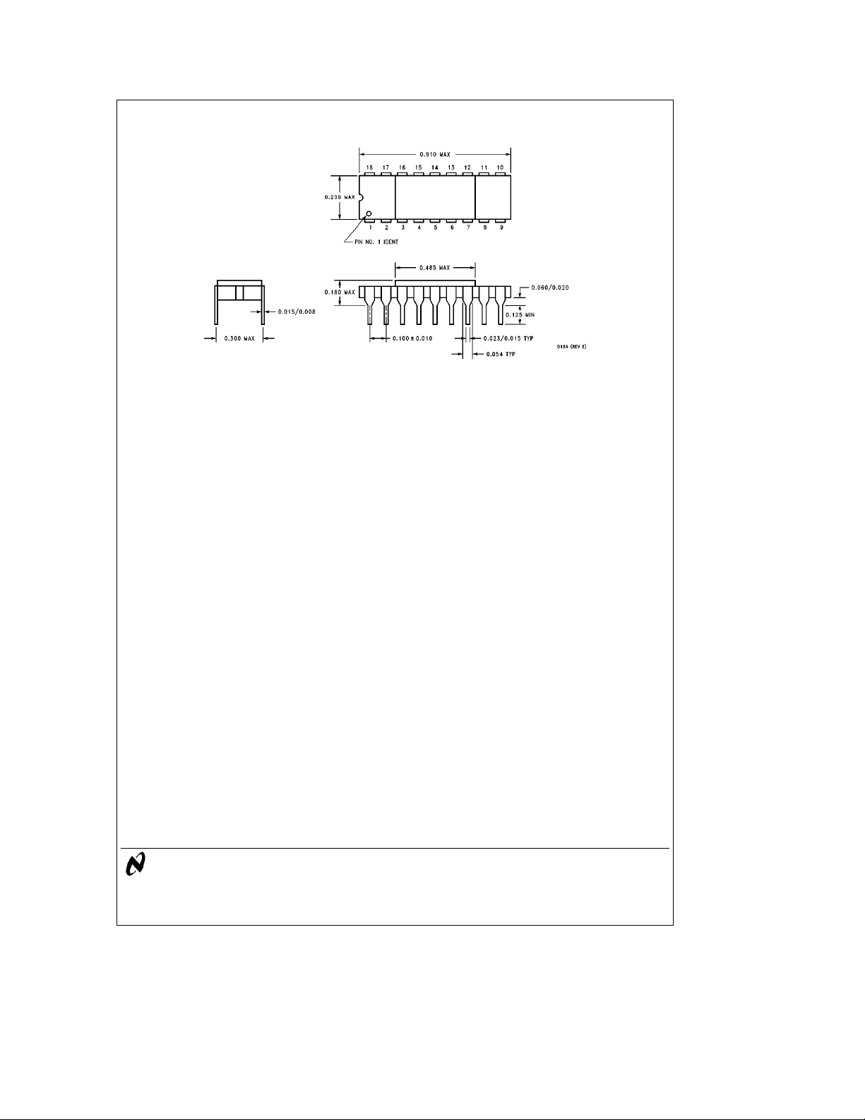
Physical Dimensions inches (millimeters)
ADC0800 8-Bit A/D Converter
Hermetic Dual-In-Line Package (D)
Order Number ADC0800PD or ADC0800PCD
NS Package Number D18A
LIFE SUPPORT POLICY
NATIONAL’S PRODUCTS ARE NOT AUTHORIZED FOR USE AS CRITICAL COMPONENTS IN LIFE SUPPORT
DEVICES OR SYSTEMS WITHOUT THE EXPRESS WRITTEN APPROVAL OF THE PRESIDENT OF NATIONAL
SEMICONDUCTOR CORPORATION. As used herein:
1. Life support devices or systems are devices or 2. A critical component is any component of a life
systems which, (a) are intended for surgical implant support device or system whose failure to perform can
into the body, or (b) support or sustain life, and whose be reasonably expected to cause the failure of the life
failure to perform, when properly used in accordance support device or system, or to affect its safety or
with instructions for use provided in the labeling, can effectiveness.
be reasonably expected to result in a significant injury
to the user.
National Semiconductor National Semiconductor National Semiconductor National Semiconductor
Corporation Europe Hong Kong Ltd. Japan Ltd.
1111 West Bardin Road Fax: (
Arlington, TX 76017 Email: cnjwge@tevm2.nsc.com Ocean Centre, 5 Canton Rd. Fax: 81-043-299-2408
Tel: 1(800) 272-9959 Deutsch Tel: (
Fax: 1(800) 737-7018 English Tel: (
National does not assume any responsibility for use of any circuitry described, no circuit patent licenses are implied and National reserves the right at any time without notice to change said circuitry and specifications.
Fran3ais Tel: (
Italiano Tel: (
a
49) 0-180-530 85 86 13th Floor, Straight Block, Tel: 81-043-299-2309
a
49) 0-180-530 85 85 Tsimshatsui, Kowloon
a
49) 0-180-532 78 32 Hong Kong
a
49) 0-180-532 93 58 Tel: (852) 2737-1600
a
49) 0-180-534 16 80 Fax: (852) 2736-9960
 Loading...