

查询54F322供应商
54F/74F322
Octal Serial/Parallel Register with Sign Extend
54F/74F322 Octal Serial/Parallel Register with Sign Extend
May 1995
General Description
The ’F322 is an 8-bit shift register with provision for either
serial or parallel loading and with TRI-STATE
puts plus a bi-state serial output. Parallel data inputs and
parallel outputs are multiplexed to minimize pin count. State
changes are initiated by the rising edge of the clock. Four
synchronous modes of operation are possible: hold (store),
shift right with serial entry, shift right with sign extend and
parallel load. An asynchronous Master Reset (MR
overrides clocked operation and clears the register.
Commercial Military
74F322PC N20A 20-Lead (0.300×Wide) Molded Dual-In-Line
54F322DM (Note 2) J20A 20-Lead Ceramic Dual-In-Line
74F322SJ (Note 1) M20D 20-Lead (0.300×Wide) Molded Small Outline, EIAJ
54F322FM (Note 2) W20A 20-Lead Cerpack
54F322LM (Note 2) E20A 20-Lead Ceramic Leadless Chip Carrier, Type C
Note 1: Devices also available in 13×reel. Use suffixeSJX.
Note 2: Military grade device with environmental and burn-in processing. Use suffix
parallel out-
É
) input
Package
Number
Features
Y
Multiplexed parallel I/O ports
Y
Separate serial input and output
Y
Sign extend function
Y
TRI-STATE outputs for bus applications
Package Description
e
DMQB, FMQB and LMQB.
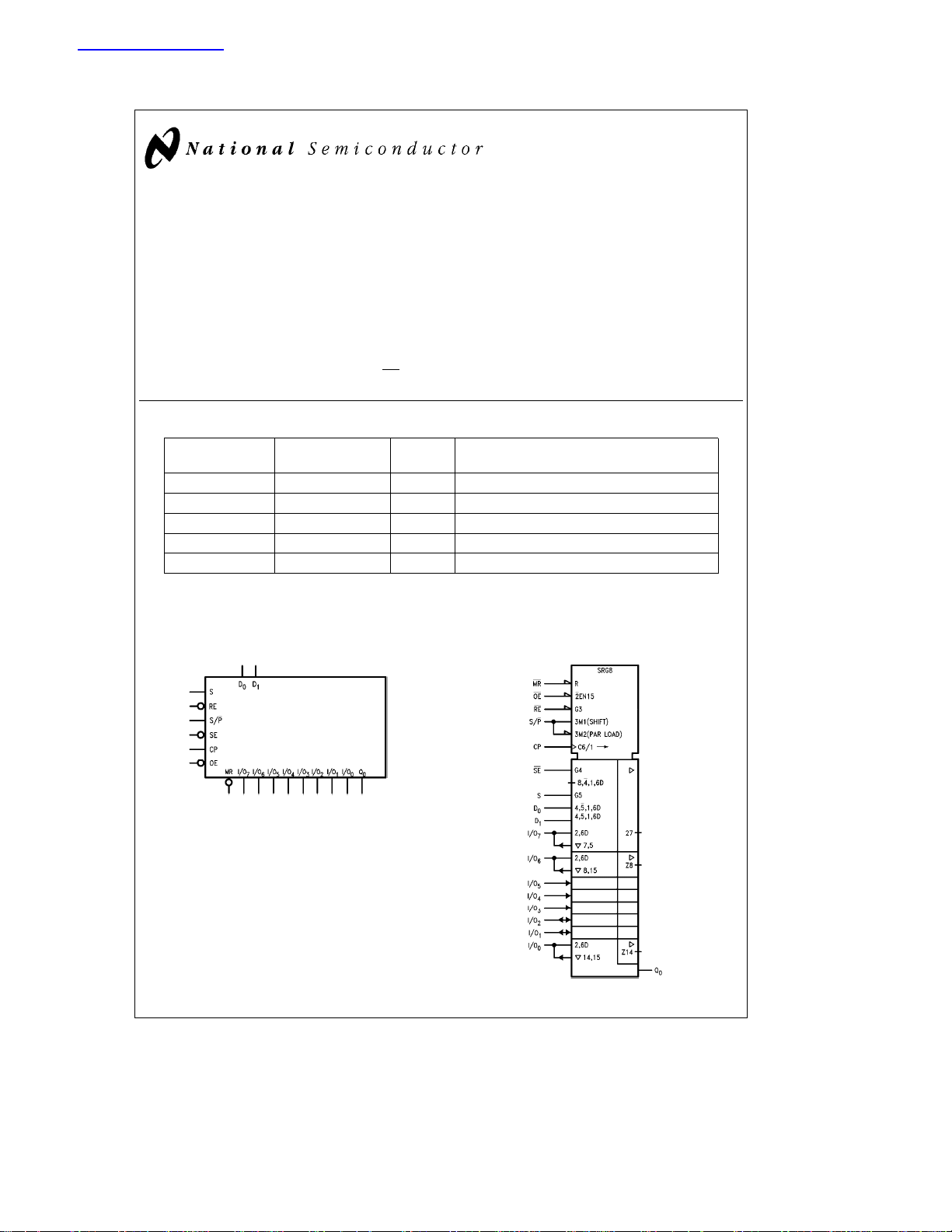
Logic Symbols
IEEE/IEC
TL/F/9516– 3
TL/F/9516– 5
TRI-STATEÉis a registered trademark of National Semiconductor Corporation.
C
1995 National Semiconductor Corporation RRD-B30M105/Printed in U. S. A.
TL/F/9516
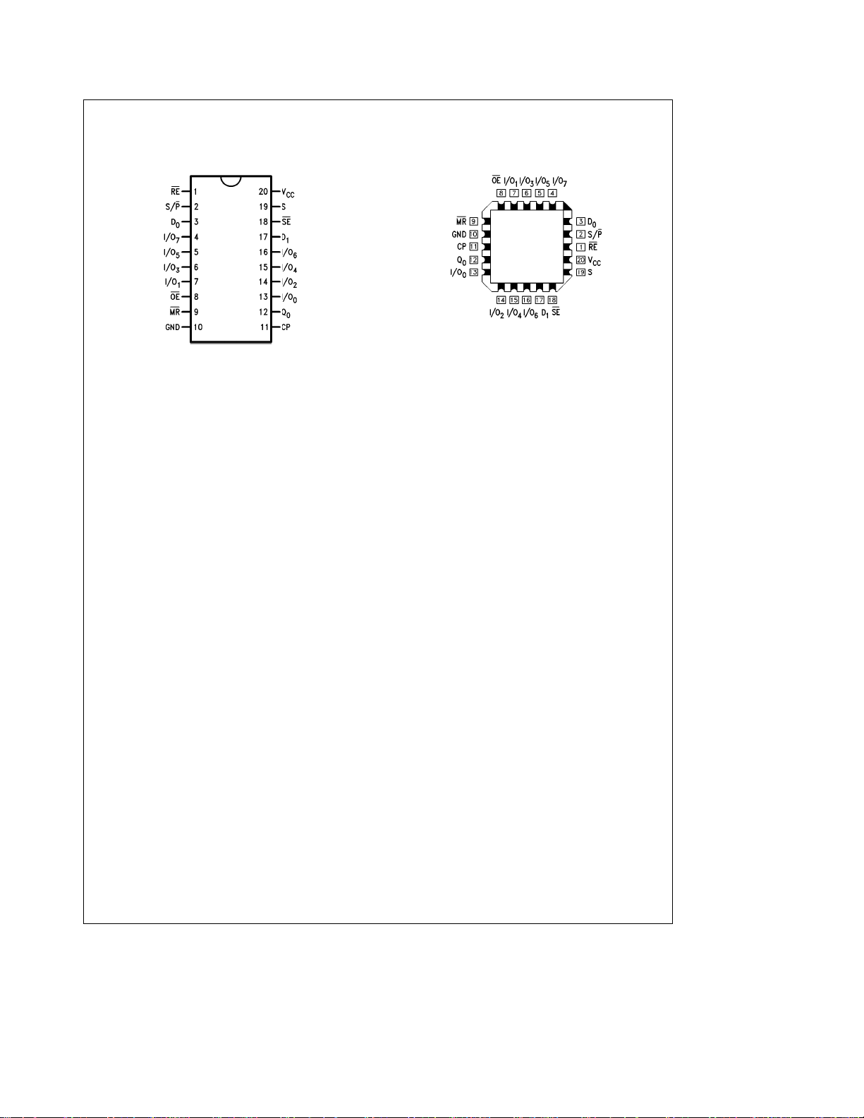
Connection Diagrams
Pin Assignment
for DIP, SOIC and Flatpak
Pin Assignment
for LCC
TL/F/9516– 2
TL/F/9516– 1
2
Unit Loading/Fan Out
54F/74F
Pin Names Description
U.L. Input I
HIGH/LOW Output IOH/I
IH/IIL
OL
RE Register Enable Input (Active LOW) 1.0/1.0 20 mA/b0.6 mA
S/P
SE
Serial (HIGH) or Parallel (LOW) Mode Control Input 1.0/1.0 20 mA/b0.6 mA
Sign Extend Input (Active LOW) 1.0/3.0 20 mA/b1.8 mA
S Serial Data Select Input 1.0/2.0 20 mA/b1.2 mA
D
0,D1
CP Clock Pulse Input (Active Rising Edge) 1.0/1.0 20 mA/b0.6 mA
MR
OE
Q
0
I/O
Serial Data Inputs 1.0/1.0 20 mA/b0.6 mA
Asynchronous Master Reset Input (Active LOW) 1.0/1.0 20 mA/b0.6 mA
TRI-STATE Output Enable Input (Active LOW) 1.0/1.0 20 mA/b0.6 mA
Bi-State Serial Output 50/33.3
–I/O7Multiplexed Parallel Data Inputs or 3.5/1.083 70 mA/b0.65 mA
0
TRI-STATE Parallel Data Outputs 150/40 (33.3)
b
1 mA/b20 mA
b
3 mA/24 mA (20 mA)
Functional Description
The ’F322 contains eight D-type edge triggered flip-flops
and the interstage gating required to perform right shift and
the intrastage gating necessary for hold and synchronous
parallel load operations. A LOW signal on RE
enables shifting or parallel loading, while a HIGH signal enables the hold
mode. A HIGH signal on S/P
enables shift right, while a
LOW signal disables the TRI-STATE output buffers and enables parallel loading. In the shift right mode a HIGH signal
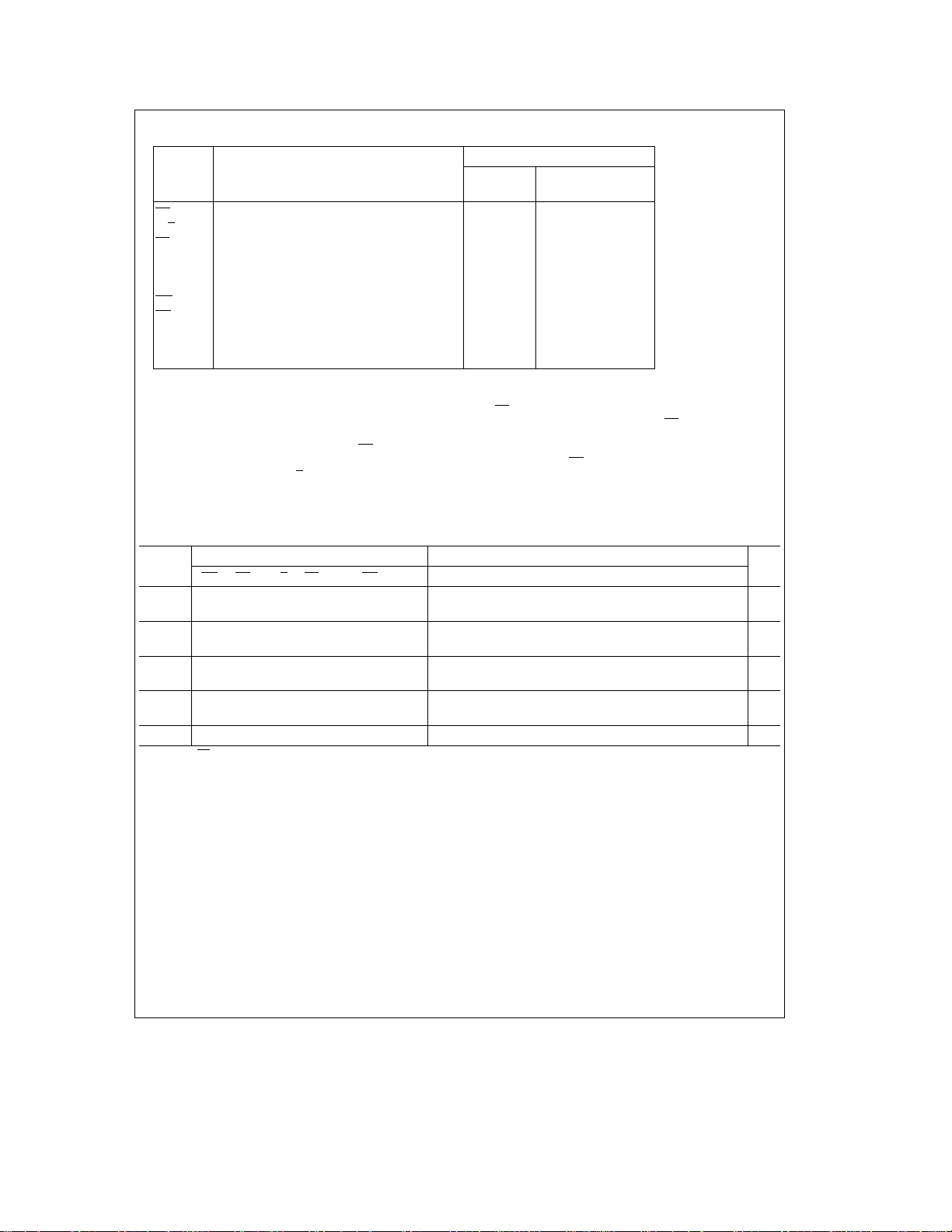
Mode Select Table
Mode
Inputs Outputs
MR RE S/P SE SOE* CP I/O7I/O6I/O5I/O4I/O3I/O2I/O1I/O
Clear L X X X X L X L L L L L L L L L
LXXXXHXZZZZZZZZL
Parallel
Load
HL L XXXLI
Shift H L H H L L L D
Right H L H H H L L D
Sign
Extend
HLHLXLLO
Hold H H X X X L L NC NC NC NC NC NC NC NC NC
*When the OE input is HIGH all I/Onterminals are at the high impedance state; sequential operation or clearing of the register is not affected.
Note 1: I
the I/O terminal.
Note 2: D
Note 3: O
H
L
Z
L
NC
e
The level of the steady-state input at the respective I/O terminal is loaded into the flip-flop while the flip-flop outputs (except Q0) are isolated from
7–I0
e
The level of the steady-state inputs to the serial multiplexer input.
0,D1
e
The level of the respective Qnflip-flop prior to the last Clock LOW-to-HIGH transition.
7–O0
e
HIGH Voltage Level
e
LOW Voltage Level
e
High Impedance Output State
e
LOW-to-HIGH Transition
e
No Change
on SE
enables serial entry from either D0or D1, as determined by the S input. A LOW signal on SE
but Q
reloads its contents, thus performing the sign extend
7
function required for the ’F384 Twos Complement Multiplier.
A HIGH signal on OE
disables the TRI-STATE output buff-
enables shift right
ers, regardless of the other control inputs. In this condition
the shifting and loading operations can still be performed.
Q
0
7I6I5I4I3I2I1I0I0
O
O
O
0
7
O
1
O7O6O5O4O3O2O1O
7
6
O
7
6
O4O
5
O
O4O
5
O
3
3
O1O
2
O
O1O
2
0
1
1
1
3
 Loading...