

查询54F240供应商
May 1995
54F/74F240
Octal Buffers/Line Drivers with TRI-STATE Outputs
54F/74F240#54F/74F241#54F/74F244
Octal Buffers/Line Drivers with TRI-STATE
General Description
The ’F240, ’F241 and ’F244 are octal buffers and line drivers designed to be employed as memory and address drivers, clock drivers and bus-oriented transmitters/receivers
which provide improved PC and board density.
Commercial Military
74F240PC N20A 20-Lead (0.300×Wide) Molded Dual-In-Line
54F240DM (Note 2) J20A 20-Lead Ceramic Dual-In-Line
74F240SC (Note 1) M20B 20-Lead (0.300×Wide) Molded Small Outline, JEDEC
74F240SJ (Note 1) M20D 20-Lead (0.300×Wide) Molded Small Outline, EIAJ
54F240FM (Note 2) W20A 20-Lead Cerpack
54F240LM (Note 2) E20A 20-Lead Ceramic Leadless Chip Carrier, Type C
74F241PC N20A 20-Lead (0.300×Wide) Molded Dual-In-Line
54F241DM (Note 2) J20A 20-Lead Ceramic Dual-In-Line
74F241SC (Note 1) M20B 20-Lead (0.300×Wide) Molded Small Outline, JEDEC
74F241SJ (Note 1) M20D 20-Lead (0.300×Wide) Molded Small Outline, EIAJ
54F241FM (Note 2) W20A 20-Lead Cerpack
54F241LM (Note 2) E20A 20-Lead Ceramic Leadless Chip Carrier, Type C
74F244PC N20A 20-Lead (0.300×Wide) Molded Dual-In-Line
54F244DM (Note 2) J20A 20-Lead Ceramic Dual-In-Line
74F244SC (Note 1) M20B 20-Lead (0.300×Wide) Molded Small Outline, JEDEC
74F244SJ (Note 1) M20D 20-Lead (0.300×Wide) Molded Small Outline, EIAJ
74F244MSA (Note 1) MSA20 20-Lead Molded Shrink Small Outline, EIAJ Type II
54F244FM (Note 2) W20A 20-Lead Cerpack
54F244LM (Note 2) E20A 20-Lead Ceramic Leadless Chip Carrier, Type C
Note 1: Devices also available in 13×reel. Use SuffixeSCX, SJX and MSAX.
Note 2: Military grade device with environmental and burn-in processing. Use suffix
Package
Number
Features
Y
TRI-STATE outputs drive bus lines or buffer memory
address registers
Y
Outputs sink 64 mA (48 mA mil)
Y
12 mA source current
Y
Input clamp diodes limit high-speed termination effects
Y
Guaranteed 4000V minimum ESD protection
Package Description
e
DMQB, FMQB and LMQB.
Outputs
É
#
54F/74F241
#
54F/74F244
TRI-STATEÉis a registered trademark of National Semiconductor Corporation.
C
1995 National Semiconductor Corporation RRD-B30M75/Printed in U. S. A.
TL/F/9501
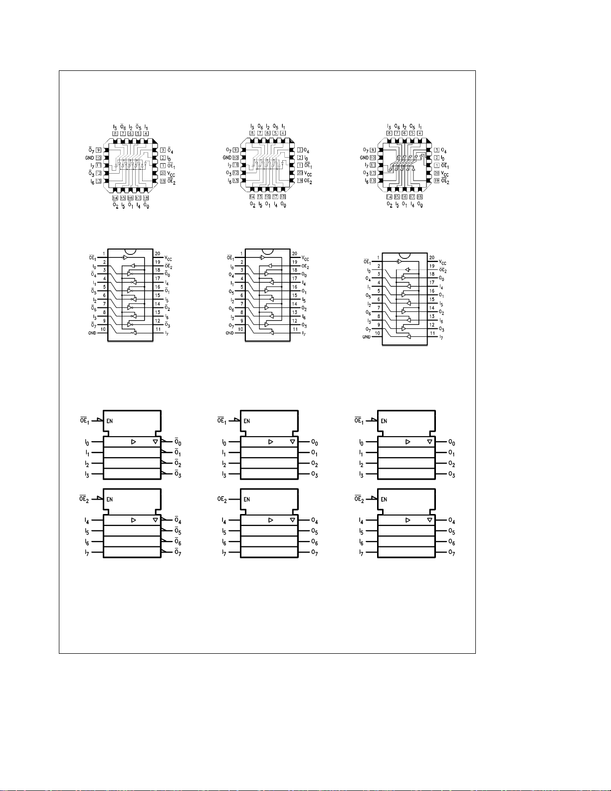
Connection Diagrams
’F240
Pin Assignment for LCC
’F241
’F244
Logic Symbols
IEEE/IEC
’F240
TL/F/9501– 2
TL/F/9501– 4
Pin Assignment for DIP, SOIC, SSOP and Flatpak
TL/F/9501– 1 TL/F/9501– 3
IEEE/IEC
’F241
TL/F/9501– 6
TL/F/9501– 5
IEEE/IEC
’F244
TL/F/9501– 7
TL/F/9501– 8
TL/F/9501– 9
2
Unit Loading/Fan Out
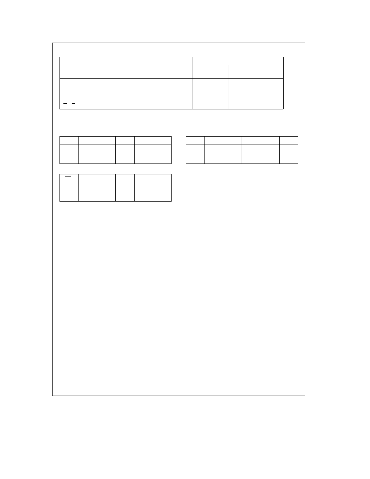
Pin Names Description
OE1,OE
2
OE
2
I
0–I7
I0–I
7
O
0–O7,O0–O7
*Worst-case ’F240 enabled; ’F241, ’F244 disabled
TRI-STATE Output Enable Input (Active LOW) 1.0/1.667 20 mA/b1mA
TRI-STATE Output Enable Input (Active HIGH) 1.0/1.667 20 mA/b1mA
Inputs (’F240) 1.0/1.667* 20 mA/b1mA
Inputs (’F241, ’F244) 1.0/2.667* 20 mA/b1.6 mA
Outputs 600/106.6 (80)
54F/74F
U.L. Input I
HIGH/LOW Output IOH/I
b
12 mA/64 mA (48 mA)
IH/IIL
OL
Truth Tables
’F240
OE
OE
D
1
O
1n
OE
1n
D
2
O
2n
HXZHXZ
LHLLHL
LLHLLH
’F241
D
1
O
1n
OE
1n
D
2
O
2n
HXZL XZ
LHHHHH
LLLHLL
’F244
2n
OE
D
1
O
1n
OE
1n
D
2
O
2n
2n
HXZHXZ
LHHLHH
LLLLLL
e
H
HIGH Voltage Level
e
LOW Voltage Level
L
e
Immaterial
2n
X
e
High Impedance
Z
3
 Loading...