

National Semiconductor 54F00, 74F00 Technical data
查询54F00供应商
December 1994
54F/74F00
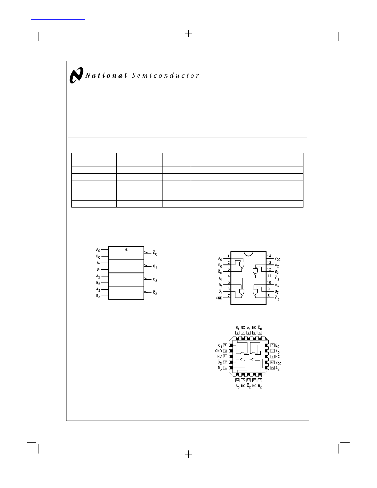
Quad 2-Input NAND Gate
General Description
This device contains four independent gates, each of which
performs the logic NAND function.
Ordering Code: See Section 0
Commercial Military Package Package Description
Number
74F00PC N14A 14-Lead (0.300" Wide) Molded Dual-In-Line
54F00DM (Note 2) J14A 14-Lead Ceramic Dual-In-Line
74F00SC (Note 1) M14A 14-Lead (0.150" Wide) Molded Small Outline, JEDEC
74F00SJ (Note 1) M14D 14-Lead (0.300" Wide) Molded Small Outline, EIAJ
54F00FM (Note 2) W14B 14-Lead Cerpack
54F00LM (Note 2) E20A 20-Lead Ceramic Leadless Chip Carrier, Type C
Note 1: Devices also available in 13" reel. Use suffix=SCX and SJX.
Note 2: Military grade device with environmental and burn-in processing. Use suffix=DMQB, FMQB and LMQB.
Logic Symbol Connection Diagrams
Features
n Guaranteed 4000V minimum ESD protection
54F/74F00 Quad 2-Input NAND Gate
54F/74F00
DSXXX
IEEE/IEC
DS009454-3
TRI-STATE®is a registered trademark of National Semiconductor Corporation.
Pin Assignment
for DIP, SOIC and Flatpak
DS009454-2
Pin Assignment
for LCC
DS009454-1
© 1997 National Semiconductor Corporation DS009454 www.national.com
PrintDate=1997/08/27 PrintTime=13:03:35 9738 ds009454 Rev. No. 1 cmserv
Proof 1
1
Unit Loading/Fan Out
See Section 0 for U.L. definitions
54F/74F
Pin Names Description U.L. Input I
HIGH/LOW Output IOH/I
An,B
O
n
n
Inputs 1.0/1.0 20 µA/−0.6 mA
Outputs 50/33.3 −1 mA/20 mA
DSXXX
IH/IIL
OL
www.national.com 2
PrintDate=1997/08/27 PrintTime=13:03:36 9738 ds009454 Rev. No. 1 cmserv Proof 2
Absolute Maximum Ratings (Note 3)
Storage Temperature −65˚C to +150˚C
Ambient Temperature under Bias −55˚C to +125˚C
Junction Temperature under Bias −55˚C to +175˚C
Plastic −55˚C to +150˚C
Pin Potential to
V
CC
Ground Pin −0.5V to +7.0V
Input Voltage (Note 4) −0.5V to +7.0V
Input Current (Note 4) −30 mA to +5.0 mA
Voltage Applied to Output
in HIGH State (with V
Standard Output −0.5V to V
TRI-STATE®Output −0.5V to +5.5V
=
0V)
CC
CC
in LOW State (Max) twice the rated I
ESD Last Passing Voltage (Min) 4000V
Recommended Operating
Conditions
Free Air Ambient Temperature
Commercial 0˚C to +70˚C
Supply Voltage
Commercial +4.5V to +5.5V
Note 3: Absolute maximum ratings are values beyond which the device may
be damaged or haveitsusefullifeimpaired.Functionaloperationunderthese
conditions is not implied.
Note 4: Either voltage limit or current limit is sufficient to protect inputs.
Current Applied to Output
DC Electrical Characteristics
Symbol Parameter 54F/74F Units V
Min Typ Max
V
V
V
V
V
I
I
I
V
I
I
I
I
I
IH
IL
CD
OH
OL
IH
BVI
CEX
ID
OD
IL
OS
CCH
CCL
Input HIGH Voltage 2.0 V Recognized as a HIGH Signal
Input LOW Voltage 0.8 V Recognized as a LOW Signal
Input Clamp Diode Voltage −1.2 V Min I
Output HIGH 54F 10%V
Voltage 74F 10%V
74F 5%V
Output LOW 54F 10%V
Voltage 74F 10%V
CC
2.5 I
CC
2.5 V Min I
CC
2.7 I
CC
CC
0.5 V Min I
0.5 I
Input HIGH 54F 20.0 µA Max V
Current 74F 5.0
Input HIGH Current 54F 100 µA Max V
Breakdown Test 74F 7.0
Output HIGH 54F 250 µA Max V
Leakage Current 74F 50
Input Leakage 74F 4.75 V 0.0 I
Test All other pins grounded
Output Leakage 74F 3.75 µA 0.0 V
Circuit Current All other pins grounded
Input LOW Current −0.6 mA Max V
Output Short-Circuit Current −60 −150 mA Max V
Power Supply Current 1.9 2.8 mA Max V
Power Supply Current 6.8 10.2 mA Max V
(mA)
OL
IN
OH
OH
OH
OL
OL
ID
IN
IN
OUT
IOD
IN
OUT
O
O
=
−18 mA
=
−1 mA
=
−1 mA
=
−1 mA
=
20 mA
=
20 mA
=
2.7V
=
7.0V
=
=
1.9 µA
=
=
0.5V
=
=
HIGH
=
LOW
Conditions
V
CC
150 mV
0V
CC
AC Electrical Characteristics
See Section 0 for Waveforms and Load Configurations
74F 54F 74F
=
+25˚C T
T
A
=
Symbol Parameter V
+5.0V C
CC
=
50 pF
C
L
Min Typ Max Min Max Min Max
t
PLH
t
PHL
Propagation Delay 2.4 3.7 5.0 2.0 7.0 2.4 6.0 ns
An,Bnto O
n
1.5 3.2 4.3 1.5 6.5 1.5 5.3
3 www.national.com
PrintDate=1997/08/27 PrintTime=13:03:42 9738 ds009454 Rev. No. 1 cmserv Proof 3
=
A,VCC
Mil T
=
50 pF C
L
=
A,VCC
Com Fig.
=
50 pF Units No.
L
kk-kk
DSXXX
DSXXX
Book
Extract
End
 Loading...