

54AC/74AC125#74ACT125
Quad Buffer with TRI-STATE
Outputs
É
54AC/74AC125
March 1993
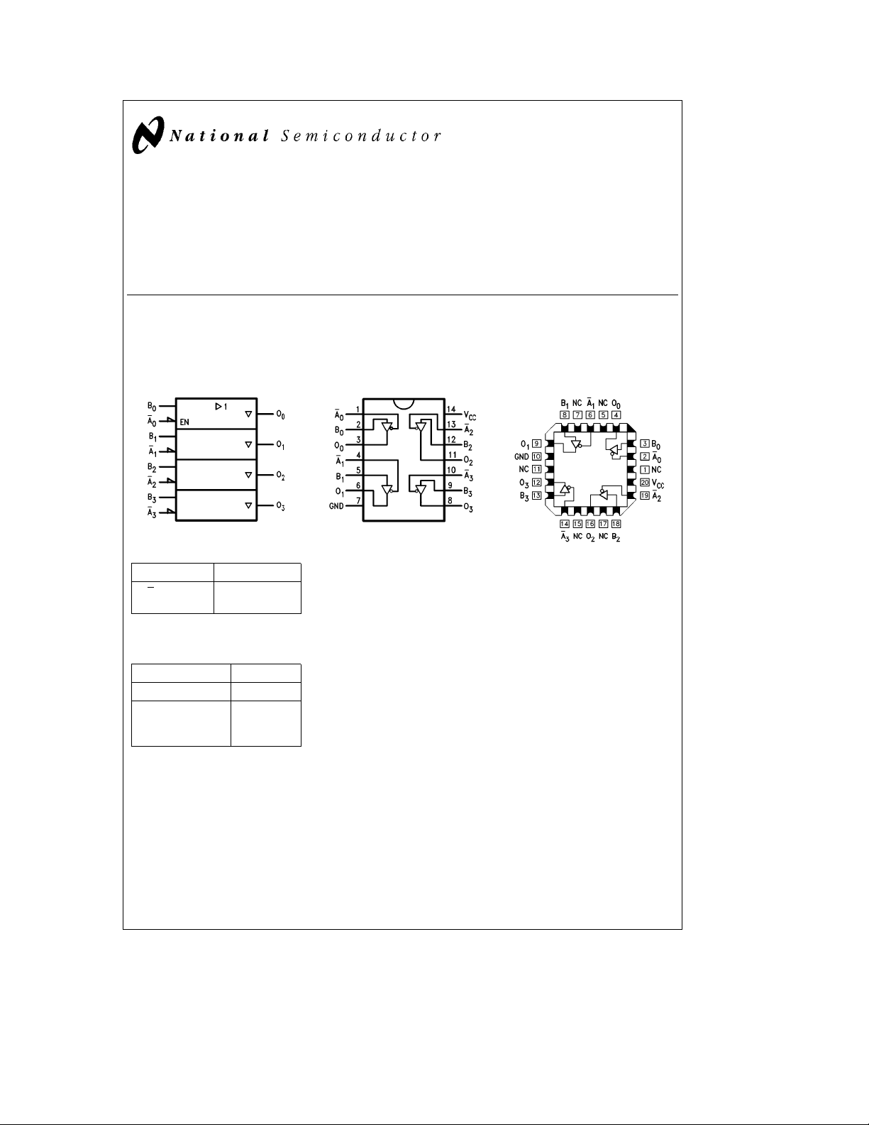
General Description
The ’AC/’ACT125 contains four independent non-inverting
buffers with TRI-STATE outputs.
Logic Symbol
IEEE/IEC
TL/F/10692– 1
Pin Names Description
A
O
n,Bn
n
Inputs
Outputs
Pin Assignment
for DIP, SOIC and Flatpak
Features
Y
ICCreduced by 50%
Y
Outputs source/sink 24 mA
Y
’ACT125 has TTL-compatible outputs
Connection Diagrams
Pin Assignment
TL/F/10692– 2
#
74ACT125 Quad Buffer with TRI-STATE Outputs
for LCC
TL/F/10692– 3
Function Table
Inputs Output
A
n
LL L
LH H
HX Z
TRI-STATEÉis a registered trademark of National Semiconductor Corporation.
TM
FACT
is a trademark of National Semiconductor Corporation.
C
1995 National Semiconductor Corporation RRD-B30M75/Printed in U. S. A.
B
n
O
n
TL/F/10692
e
H
HIGH Voltage Level
e
LOW Voltage Level
L
e
HIGH Impedance
Z
e
Immaterial
X
Absolute Maximum Ratings (Note 1)
If Military/Aerospace specified devices are required,
please contact the National Semiconductor Sales
Office/Distributors for availability and specifications.
b
0.5V to V
b
0.5V to V
b
0.5V toa7.0V
b
a
a
CC
b
a
a
CC
20 mA
20 mA
0.5V
20 mA
20 mA
0.5V
Supply Voltage (V
DC Input Diode Current (IK)
eb
V
0.5V
I
e
V
V
I
CC
)
CC
a
0.5V
DC Input Voltage (VI)
DC Output Diode Current (IOK)
eb
V
0.5V
O
e
V
a
V
CC
0.5V
O
DC Output Voltage (VO)
DC Output Source
or Sink Current (I
)
O
g
50 mA
DC VCCor Ground Current
per Output Pin (I
Storage Temperature (T
Junction Temperature (T
CDIP 175
CC
or I
GND
STG
J
)
)
b
)
PDIP 140
Note 1: Absolute maximum ratings are those values beyond which damage
to the device may occur. The databook specifications should be met, without
exception, to ensure that the system design is reliable over its power supply,
temperature, and output/input loading variables. National does not recommend operation of FACT
TM
circuits outside databook specifications.
g
50 mA
65§Ctoa150§C
C
§
C
§
DC Characteristics for ’AC Family Devices
74AC 54AC 74AC
V
Symbol Parameter
V
Minimum High Level 3.0 1.5 2.1 2.1 2.1 V
IH
Input Voltage 4.5 2.25 3.15 3.15 3.15 V or V
(V)
CC
5.5 2.75 3.85 3.85 3.85
V
Maximum Low Level 3.0 1.5 0.9 0.9 0.9 V
IL
Input Voltage 4.5 2.25 1.35 1.35 1.35 V or V
5.5 2.75 1.65 1.65 1.65
V
Minimum High Level 3.0 2.99 2.9 2.9 2.9 I
OH
Output Voltage 4.5 4.49 4.4 4.4 4.4 V
5.5 5.49 5.4 5.4 5.4
3.0 2.56 2.4 2.46
4.5 3.86 3.7 3.76 V I
5.5 4.86 4.7 4.76
V
Maximum Low Level 3.0 0.002 0.1 0.1 0.1 I
OL
Output Voltage 4.5 0.001 0.1 0.1 0.1 V
5.5 0.001 0.1 0.1 0.1
3.0 0.36 0.50 0.44 12 mA
4.5 0.36 0.50 0.44 V I
5.5 0.36 0.50 0.44 24 mA
I
IN
Maximum Input
Leakage Current
*All outputs loaded; thresholds on input associated with output under test.
5.5
ea
T
25§C
A
b
55§Ctoa125§Cb40§Ctoa85§C
Typ Guaranteed Limits
g
0.1
Recommended Operating
Conditions
Supply Voltage (VCC)
’AC 2.0V to 6.0V
’ACT 4.5V to 5.5V
Input Voltage (V
Output Voltage (VO) 0VtoV
Operating Temperature (TA)
74AC/ACT
54AC/ACT
Minimum Input Edge Rate (DV/Dt)
’AC Devices
V
from 30% to 70% of V
IN
V
CC
Minimum Input Edge Rate (DV/Dt)
’ACT Devices
V
from 0.8V to 2.0V
IN
V
CC
e
T
A
g
1.0
) 0VtoV
I
b
40§Ctoa85§C
b
55§Ctoa125§C
@
3.3V, 4.5V, 5.5V 125 mV/ns
@
4.5V, 5.5V 125 mV/ns
CC
e
T
A
g
1.0 mA
Units Conditions
e
OUT
b
CC
e
OUT
b
CC
eb
OUT
e
*V
VILor V
IN
OH
e
50 mA
OUT
e
*V
VILor V
IN
OL
e
VCC, GND
V
I
0.1V
0.1V
0.1V
0.1V
50 mA
b
12 mA
b
24 mA
b
24 mA
24 mA
CC
CC
IH
IH
2
DC Characteristics for ’AC Family Devices (Continued)
74AC 54AC 74AC
Symbol Parameter
V
(V)
CC
ea
T
25§C
A
b
e
T
A
55§Ctoa125§Cb40§Ctoa85§C
Typ Guaranteed Limits
I
OZ
I
OLD
I
OHD
I
CC
Maximum TRI-STATE VI(OE)eVIL,V
Current 5.5
²
Minimum Dynamic 5.5 50 75 mA V
Output Current
Maximum Quiescent
Supply Current or GND
²
Maximum test duration 2.0 ms, one output loaded at a time.
Note : I
@
and I
IN
I
CC
3.0V are guaranteed to be less than or equal to the respective limit@5.5V VCC.
CC
for 54AC@25§C is identical to 74AC@25§C.
5.5
5.5 4.0 80.0 40.0 mA
g
0.5
g
10.0
b
50
DC Characteristics for ’ACT Family Devices
74ACT 74ACT
V
Symbol Parameter
V
IH
V
IL
V
OH
Minimum High Level 4.5 1.5 2.0 2.0
Input Voltage 5.5 1.5 2.0 2.0 or V
Maximum Low Level 4.5 1.5 0.8 0.8
Input Voltage 5.5 1.5 0.8 0.8 or V
Minimum High Level 4.5 4.49 4.4 4.4
Output Voltage 5.5 5.49 5.4 5.4
(V)
CC
4.5 3.86 3.76
5.5 4.86 4.76
V
OL
Maximum Low Level 4.5 0.001 0.1 0.1
Output Voltage 5.5 0.001 0.1 0.1
4.5 0.36 0.44
5.5 0.36 0.44 24 mA
I
IN
I
OZ
I
CCT
I
OLD
I
OHD
I
CC
*All outputs loaded; thresholds on input associated with output under test.
²
Maximum test duration 2.0 ms, one output loaded at a time.
³
May be measured per the JEDEC Alternate Method.
Maximum Input Leakage Current 5.5
Maximum TRI-STATE
Current V
5.5
Maximum ICC/Input 5.5 0.6 1.5 mA V
²
Minimum Dynamic 5.5 75 mA V
Output Current
Maximum Quiescent
Supply Current or GND
5.5
5.5 4.0 40.0 mA
ea
T
25§C
A
Typ Guaranteed Limits
g
0.1
g
0.5
e
T
A
g
5.0 mAV
b
75 mA V
e
T
A
b
40§Ctoa85§C
g
1.0 mAV
g
5.0 mA
b
75 mA V
Units Conditions
e
VCC,V
V
V
I
O
OLD
OHD
IN
e
VCC, GND
e
e
e
V
CC
GND
1.65V Max
3.85V Min
Units Conditions
e
V
0.1V
OUT
V
V
V
VI
V
VI
V
I
*V
I
*V
V
V
OUT
OH
OUT
OL
OUT
IN
IN
I
I
O
I
OLD
OHD
IN
b
CC
e
b
CC
eb
e
VILor V
e
50 mA
e
VILor V
e
VCC, GND
e
VIL,V
e
VCC, GND
e
V
CC
e
e
e
V
0.1V
0.1V
0.1V
50 mA
b
b
IH
b
2.1V
1.65V Max
3.85V Min
CC
IH
IH
24 mA
24 mA
IH
24 mA
³
3
 Loading...