

National Semiconductor 54F20, 74F20 Technical data
查询54F20供应商
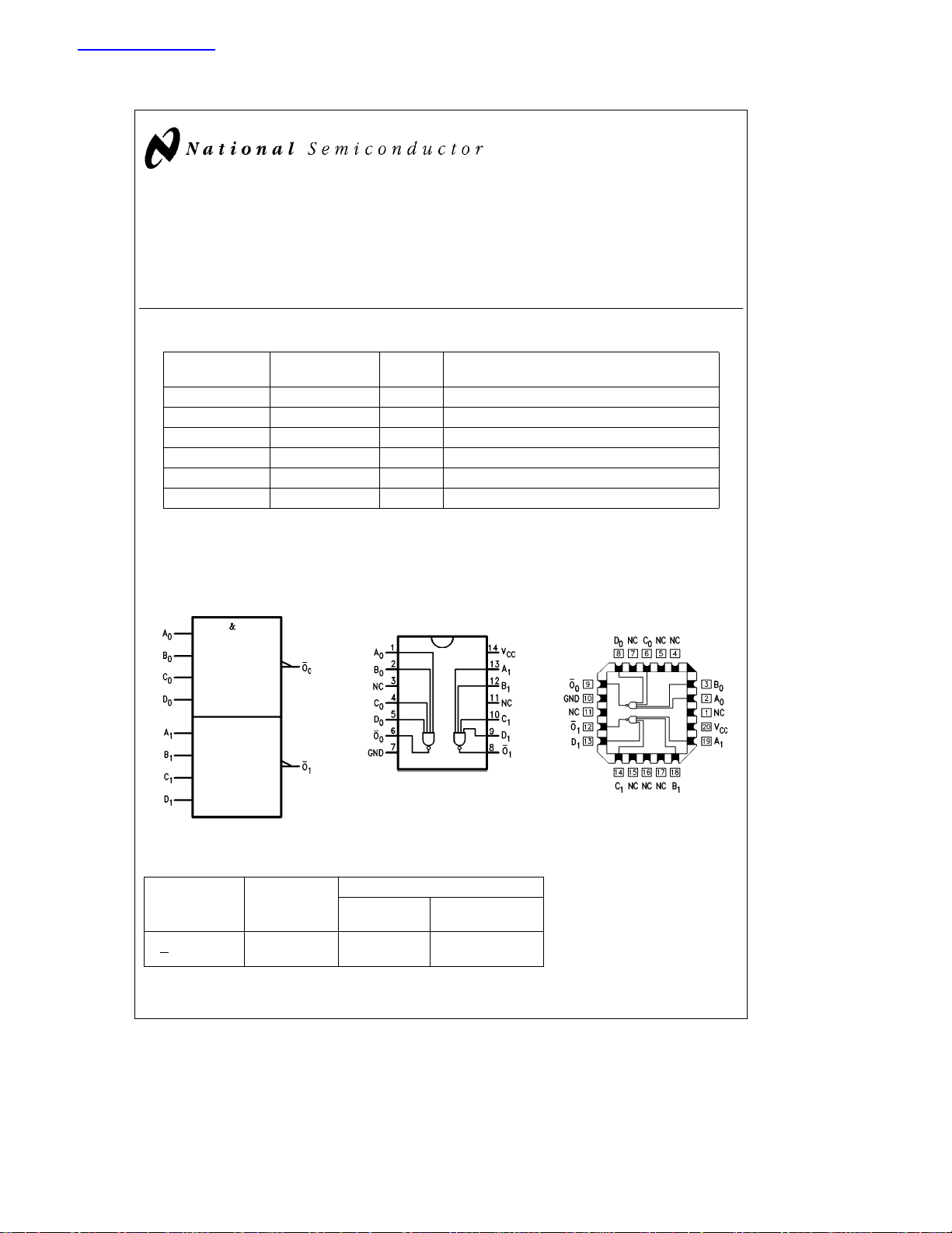
54F/74F20
Dual 4-Input NAND Gate
General Description
This device contains two independent gates, each of which
performs the logic NAND function.
54F/74F20 Dual 4-Input NAND Gate
November 1994
Commercial Military
74F20PC N14A 14-Lead (0.300×Wide) Molded Dual-In-Line
54F20DM (Note 2) J14A 14-Lead Ceramic Dual-In-Line
74F20SC (Note 1) M14A 14-Lead (0.150×Wide) Molded Small Outline, JEDEC
74F20SJ (Note 1) M14D 14-Lead (0.300×Wide) Molded Small Outline, EIAJ
54F20FM (Note 2) W14B 14-Lead Cerpack
54F20LM (Note 2) E20A 20-Lead Ceramic Leadless Chip Carrier, Type C
Note 1: Devices also available in 13×reel. Use suffixeSCX and SJX.
Note 2: Military grade device with environmental and burn-in processing. Use suffix
Logic Symbol
IEEE/IEC
TL/F/9462– 3
Package
Number
e
Connection Diagrams
Pin Assignment
for DIP, SOIC and Flatpak
TL/F/9462– 2
Package Description
DMQB, FMQB and LMQB.
Pin Assignment
for LCC
TL/F/9462– 1
Unit Loading/Fan Out
54F/74F
Pin Names Description
An,Bn,Cn,D
O
n
TRI-STATEÉis a registered trademark of National Semiconductor Corporation.
C
1995 National Semiconductor Corporation RRD-B30M75/Printed in U. S. A.
Inputs 1.0/1.0 20 mA/b0.6 mA
n
Outputs 50/33.3
TL/F/9462
U.L. Input I
HIGH/LOW Output IOH/I
b
1 mA/20 mA
IH/IIL
OL
Absolute Maximum Ratings (Note 1)
If Military/Aerospace specified devices are required,
please contact the National Semiconductor Sales
Office/Distributors for availability and specifications.
Storage Temperature
Ambient Temperature under Bias
Junction Temperature under Bias
Plastic
Pin Potential to
V
CC
Ground Pin
Input Voltage (Note 2)
Input Current (Note 2)
Voltage Applied to Output
in HIGH State (with V
Standard Output
CC
e
TRI-STATEÉOutput
0V)
b
65§Ctoa150§C
b
55§Ctoa125§C
b
55§Ctoa175§C
b
55§Ctoa150§C
b
0.5V toa7.0V
b
0.5V toa7.0V
b
30 mA toa5.0 mA
b
0.5V to V
b
0.5V toa5.5V
Current Applied to Output
in LOW State (Max) twice the rated I
Note 1: Absolute maximum ratings are values beyond which the device may
be damaged or have its useful life impaired. Functional operation under
these conditions is not implied.
Note 2: Either voltage limit or current limit is sufficient to protect inputs.
(mA)
OL
DC Electrical Characteristics
Symbol Parameter
V
V
V
V
V
I
IH
I
BVI
I
CEX
V
I
OD
I
IL
I
OS
I
CCH
I
CCL
IH
IL
CD
OH
OL
ID
Input HIGH Voltage 2.0 V Recognized as a HIGH Signal
Input LOW Voltage 0.8 V Recognized as a LOW Signal
Input Clamp Diode Voltage
Output HIGH 54F 10% V
Voltage 74F 10% V
Output LOW 54F 10% V
Voltage 74F 10% V
Input HIGH 54F 20.0
Current 74F 5.0
Input HIGH Current 54F 100
Breakdown Test 74F 7.0
Output HIGH 54F 250
Leakage Current 74F 50
Input Leakage
Test All other pins grounded
Output Leakage
Circuit Current All other pins grounded
Input LOW Current
Output Short-Circuit Current
Power Supply Current 0.9 1.4 mA Max V
Power Supply Current 3.4 5.1 mA Max V
74F 5% V
74F 4.75 V 0.0
74F 3.75 mA 0.0
Min Typ Max
2.5 I
CC
2.5 V Min I
CC
2.7 I
CC
CC
CC
b
60
CC
54F/74F
Recommended Operating
Conditions
Free Air Ambient Temperature
Military
Commercial 0
Supply Voltage
Military
Commercial
Units V
b
1.2 V Min I
0.5
0.5 I
CC
V Min
mA Max V
mA Max V
mA Max V
b
0.6 mA Max V
b
150 mA Max V
I
I
V
IN
OH
OH
OH
OL
OL
ID
IN
IN
OUT
IOD
IN
OUT
O
O
eb
eb
eb
eb
e
e
e
e
e
e
1.9 mA
e
e
e
e
e
20 mA
20 mA
HIGH
LOW
Conditions
18 mA
1mA
1mA
1mA
2.7V
7.0V
V
150 mV
0.5V
0V
b
55§Ctoa125§C
Ctoa70§C
§
a
4.5V toa5.5V
a
4.5V toa5.5V
CC
2
 Loading...