

National Semiconductor 54F161A, 74F161A Technical data
查询54F161ADM供应商
54F/74F161A#54F/74F163A
Synchronous Presettable Binary Counter
General Description
The ’F161A and ’F163A are high-speed synchronous modulo-16 binary counters. They are synchronously presettable
for application in programmable dividers and have two types
of Count Enable inputs plus a Terminal Count output for
versatility in forming synchronous multi-stage counters. The
’F161A has an asynchronous Master-Reset input that overrides all other inputs and forces the outputs LOW. The
’F163A has a Synchronous Reset input that overrides
counting and parallel loading and allows the outputs to be
simultaneously reset on the rising edge of the clock. The
’F161A and ’F163A are high-speed versions of the ’F161
and ’F163.
Features
Y
Synchronous counting and loading
Y
High-speed synchronous expansion
Y
Typical count frequency of 120 MHz
Y
Guaranteed 4000V minimum ESD protection
54F/74F161A
November 1994
#
54F/74F163A Synchronous Presettable Binary Counter
Commercial Military
74F161APC N16E 16-Lead (0.300×Wide) Molded Dual-In-Line
54F161ADM (Note 2) J16A 16-Lead Ceramic Dual-In-Line
74F161ASC (Note 1) M16A 16-Lead (0.150×Wide) Molded Small Outline, JEDEC
74F161ASJ (Note 1) M16D 16-Lead (0.300×Wide) Molded Small Outline, EIAJ
54F161AFM (Note 2) W16A 16-Lead Cerpack
54F161ALM (Note 2) E20A 20-Lead Ceramic Leadless Chip Carrier, Type C
74F163APC N16E 16-Lead (0.300×Wide) Molded Dual-In-Line
54F163ADM (Note 2) J16A 16-Lead Ceramic Dual-In-Line
74F163ASC (Note 1) M16A 16-Lead (0.150×Wide) Molded Small Outline, JEDEC
74F163ASJ (Note 1) M16D 16-Lead (0.300×Wide) Molded Small Outline, EIAJ
54F163AFM (Note 2) W16A 16-Lead Cerpack
54F163ALM (Note 2) E20A 20-Lead Ceramic Leadless Chip Carrier, Type C
Note 1: Devices also available in 13×reel. Use suffixeSCX and SJX.
Note 2: Military grade device with environmental and burn-in processing. Use suffix
Package
Number
Package Description
e
DMQB, FMQB and LMQB.
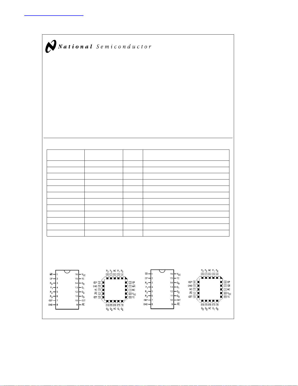
Connection Diagrams
Pin Assignment
for DIP, SOIC and Flatpak
’F161A
Pin Assignment
for LCC
’F161A
Pin Assignment
for DIP, SOIC and Flatpak
’F163A
Pin Assignment
for LCC
’F163A
TRI-STATEÉis a registered trademark of National Semiconductor Corporation.
C
1995 National Semiconductor Corporation RRD-B30M75/Printed in U. S. A.
TL/F/9486– 1
TL/F/9486
TL/F/9486– 2
TL/F/9486– 7
TL/F/9486– 8
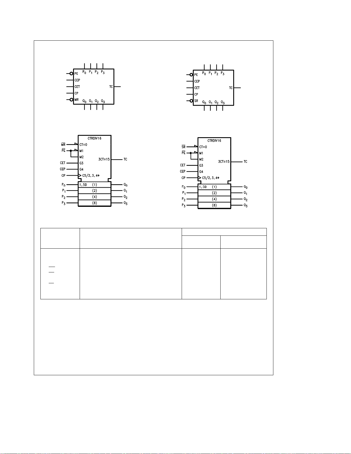
Logic Symbols
’F161A
’F163A
TL/F/9486– 3
IEEE/IEC
’F161A
TL/F/9486– 6
IEEE/IEC
’F163A
Unit Loading/Fan Out
54F/74F
Pin Names Description
CEP Count Enable Parallel Input 1.0/1.0 20 mA/b0.6 mA
CET Count Enable Trickle Input 1.0/2.0 20 mA/
CP Clock Pulse Input (Active Rising Edge) 1.0/1.0 20 mA/
MR (’F161A) Asynchronous Master Reset Input (Active LOW) 1.0/1.0 20 mA/b0.6 mA
SR
(’F163A) Synchronous Reset Input (Active LOW) 1.0/2.0 20 mA/b1.2 mA
P0–P
3
PE
Q
0–Q3
TC Terminal Count Output 50/33.3
Parallel Data Inputs 1.0/1.0 20 mA/b0.6 mA
Parallel Enable Input (Active LOW) 1.0/2.0 20 mA/b1.2 mA
Flip-Flop Outputs 50/33.3
U.L. Input I
HIGH/LOW Output IOH/I
b
1 mA/20 mA
b
1 mA/20 mA
TL/F/9486– 9
TL/F/9486– 10
IH/IIL
b
1.2 mA
b
0.6 mA
OL
2
Functional Description
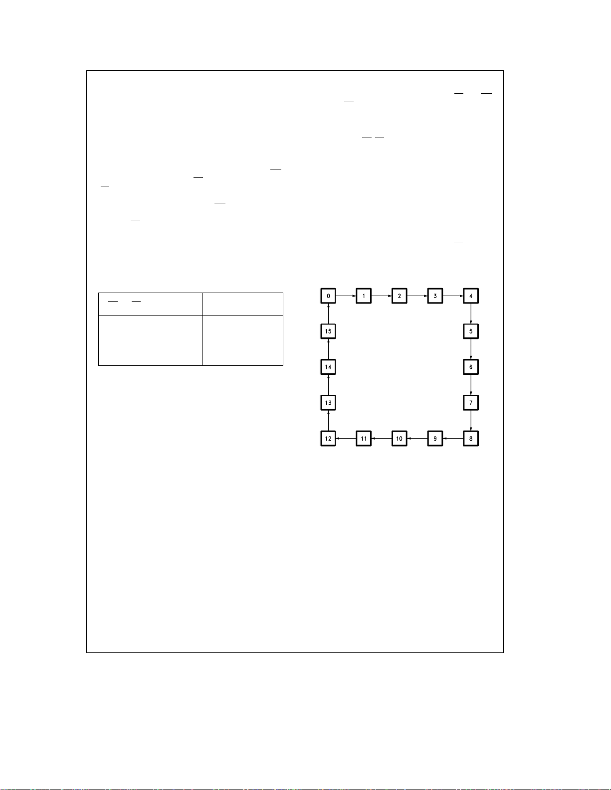
The ’F161A and ’F163A count in modulo-16 binary sequence. From state 15 (HHHH) they increment to state 0
(LLLL). The clock inputs of all flip-flops are driven in parallel
through a clock buffer. Thus all changes of the Q outputs
(except due to Master Reset of the ’F161A) occur as a result of, and synchronous with, the LOW-to-HIGH transition
of the CP input signal. The circuits have four fundamental
modes of operation, in order of precedence: asynchronous
reset (’F161A), synchronous reset (’F163A), parallel load,
count-up and hold. Five control inputsÐMaster Reset (MR
’F161A), Synchronous Reset (SR
(PE
), Count Enable Parallel (CEP) and Count Enable Trickle
(CET)Ðdetermine the mode of operation, as shown in the
Mode Select Table. A LOW signal on MR
inputs and asynchronously forces all outputs LOW. A LOW
signal on SR
overrides counting and parallel loading and
allows all outputs to go LOW on the next rising edge of CP.
A LOW signal on PE
overrides counting and allows informa-
tion on the Parallel Data (P
, ’F163A), Parallel Enable
overrides all other
) inputs to be loaded into the
n
flip-flops on the next rising edge of CP. With PE
(’F161A) or SR (’F163A) HIGH, CEP and CET permit counting when both are HIGH. Conversely, a LOW signal on either CEP or CET inhibits counting.
The ’F161A and ’F163A use D-type edge triggered flip-flops
and changing the SR
,PE, CEP and CET inputs when the CP
is in either state does not cause errors, provided that the
recommended setup and hold times, with respect to the rising edge of CP, are observed.
,
The Terminal Count (TC) output is HIGH when CET is HIGH
and the counter is in state 15. To implement synchronous
multi-stage counters, the TC outputs can be used with the
CEP and CET inputs in two different ways. Please refer to
the ’F568 data sheet. The TC output is subject to decoding
spikes due to internal race conditions and is therefore not
recommended for use as a clock or asynchronous reset for
flip-flops, counters or registers.
Q
#
0
e
CEP#CET#PE
Q
Q
#
#
1
2
3
Logic Equations: Count Enable
TCeQ
#
and MR
CET
Mode Select Table
*SR PE CET CEP
Action on the Rising
Clock Edge (L)
L X X X Reset (Clear)
H L X X Load (P
H H H H Count (Increment)
n
H H L X No Change (Hold)
H H X L No Change (Hold)
*For ’F163A only
e
HIGH Voltage Level
H
e
LOW Voltage Level
L
e
Immaterial
X
x
State Diagram
Qn)
TL/F/9486– 5
3
 Loading...