

National Semiconductor 54F14, 74F14 Technical data
查询54F14供应商
54F/74F14
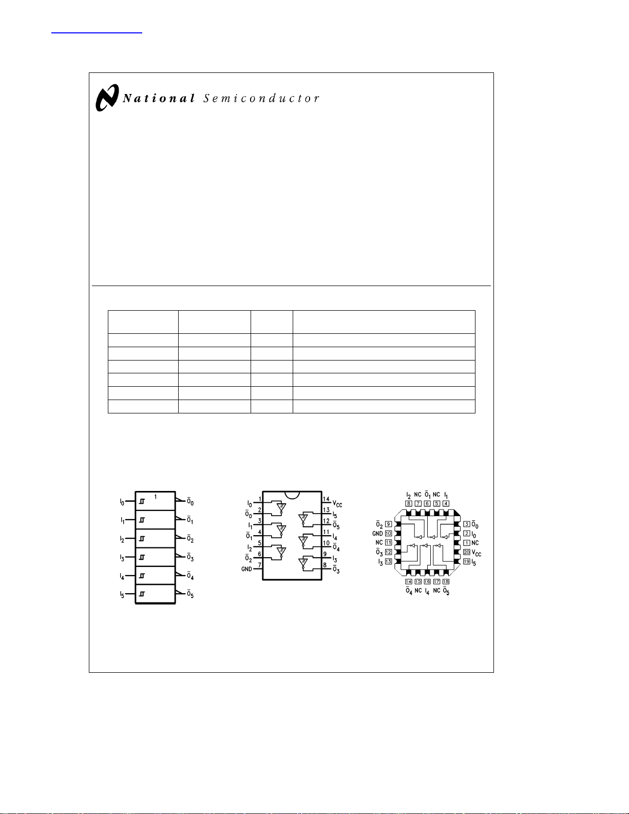
Hex Inverter Schmitt Trigger
General Description
The ’F14 contains six logic inverters which accept standard
TTL input signals and provide standard TTL output levels.
They are capable of transforming slowly changing input signals into sharply defined, jitter-free output signals. In addition, they have a greater noise margin than conventional
inverters.
Each circuit contains a Schmitt trigger followed by a Darlington level shifter and a phase splitter driving a TTL totempole output. The Schmitt trigger uses positive feed back to
December 1994
effectively speed-up slow input transition, and provide different input threshold voltages for positive and negative-going
transitions. This hysteresis between the positive-going and
negative-going input thresholds (typically 800 mV) is determined internally by resistor ratios and is essentially insensitive to temperature and supply voltage variations.
Features
Y
Guaranteed 4000V minimum ESD protection
Y
Standard Military Drawing
Ð 5962-88752
54F/74F14 Hex Inverter Schmitt Trigger
Commercial Military
74F14PC N14A 14-Lead (0.300×Wide) Molded Dual-In-Line
54F14DM (Note 2) J14A 14-Lead Ceramic Dual-In-Line
74F14SC (Note 1) M14A 14-Lead (0.150×Wide) Molded Small Outline, JEDEC
74F14SJ (Note 1) M14D 14-Lead (0.300×Wide) Molded Small Outline, EIAJ
54F14FM (Note 2) W14B 14-Lead Cerpack
54F14LM (Note 2) E20A 20-Lead Ceramic Leadless Chip Carrier, Type C
Note 1: Devices also available in 13×reel. Use SuffixeSCX and SJX.
Note 2: Military grade device with environmental and burn-in processing. Use suffix
Logic Symbol
IEEE/IEC
TL/F/9461– 3
Package
Number
Connection Diagrams
Pin Assignment
DIP, SOIC and Flatpak
Package Description
e
DMQB, FMQB and LMQB.
TL/F/9461– 1
Pin Assignment
for LCC
TL/F/9461– 2
TRI-STATEÉis a registered trademark of National Semiconductor Corporation.
C
1995 National Semiconductor Corporation RRD-B30M75/Printed in U. S. A.
TL/F/9461
Unit Loading/Fan Out
Pin Names Description
I
n
O
n
Function Table
Input Output
AO
LH
HL
e
H
HIGH Voltage Level
e
LOW Voltage Level
L
Input 1.0/1.0 20 mA/b0.6 mA
Output 50/33.3
54F/74F
U.L. Input I
HIGH/LOW Output IOH/I
b
1 mA/20 mA
IH/IIL
OL
2
Absolute Maximum Ratings (Note 1)
If Military/Aerospace specified devices are required,
please contact the National Semiconductor Sales
Office/Distributors for availability and specifications.
Storage Temperature
Ambient Temperature under Bias
Junction Temperature under Bias
VCCPin Potential to
Ground Pin
Input Voltage (Note 2)
Input Current (Note 2)
Voltage Applied to Output
in HIGH State (with V
Standard Output
CC
e
TRI-STATEÉOutput
0V)
b
65§Ctoa150§C
b
55§Ctoa125§C
b
55§Ctoa175§C
b
0.5V toa7.0V
b
0.5V toa7.0V
b
30 mA toa5.0 mA
b
0.5V to V
b
0.5V toa5.5V
Current Applied to Output
in LOW State (Max) twice the rated I
(mA)
OL
ESD Last Passing Voltage (Min) 4000V
Note 1: Absolute maximum ratings are values beyond which the device may
be damaged or have its useful life impaired. Functional operation under
these conditions is not implied.
Note 2: Either voltage limit or current limit is sufficient to protect inputs.
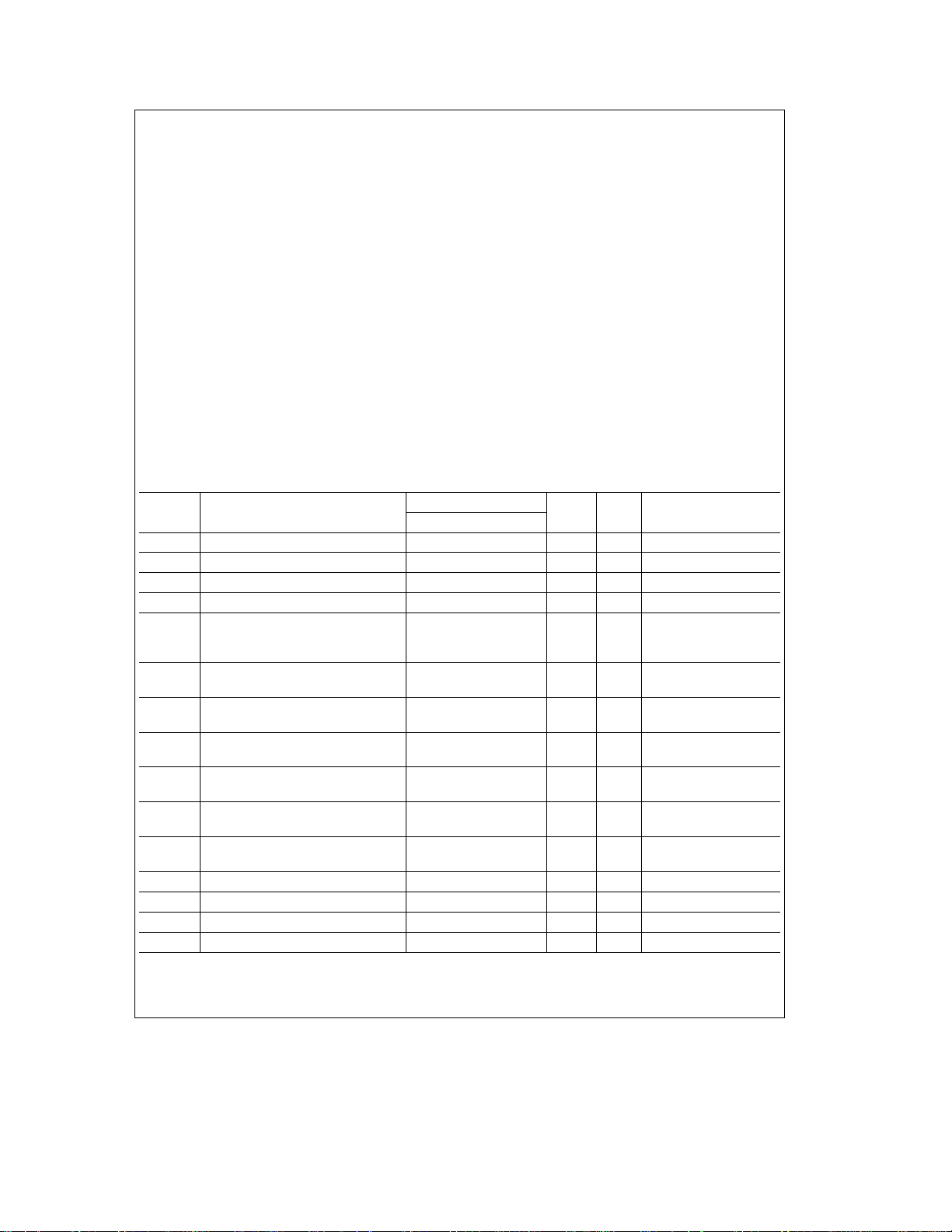
DC Electrical Characteristics
Symbol Parameter
V
V
DV
V
V
V
I
IH
I
BVI
I
CEX
V
I
OD
I
IL
I
OS
I
CCH
I
CCL
T
T
CD
OH
OL
ID
a
b
T
Positive-Going Threshold 1.5 1.7 2.0 V 5.0V
Negative-Going Threshold 0.7 0.9 1.1 V 5.0V
Hysteresis (V
–V
a
b
T
T
Input Clamp Diode Voltage
Output HIGH 54F 10% V
Voltage 74F 10% V
Output LOW 54F 10% V
Voltage 74F 10% V
Input HIGH 54F 20.0
Current 74F 5.0
Input HIGH Current 54F 100
Breakdown Test 74F 7.0
Output HIGH 54F 250
Leakage Current 74F 50
Input Leakage
Test All Other Pins Grounded
Output Leakage
Circuit Current All Other Pins Grounded
Input LOW Current
Output Short-Circuit Current
Power Supply Current 25 mA Max V
Power Supply Current 25 mA Max V
) 0.4 0.8 V 5.0V
74F 5% V
74F 4.75 V Max
74F 3.75 mA 0.0
Min Typ Max
2.5 I
CC
2.5 V Min I
CC
CC
2.7 I
CC
CC
b
CC
60
Recommended Operating
Conditions
Free Air Ambient Temperature
Military
Commercial 0
Supply Voltage
Military
Commercial
54F/74F
b
b
b
Units V
CC
1.2 V Min I
0.5
0.5 I
V Min
mA Max
mA Max
mA Max
0.6 mA Max V
150 mA Max V
IN
OH
OH
OH
I
OL
OL
V
IN
V
IN
V
OUT
I
ID
V
IOD
IN
OUT
O
O
b
Conditions
eb
eb
eb
eb
e
e
e
e
e
e
1.9 mA
e
e
e
e
HIGH
e
LOW
55§Ctoa125§C
Ctoa70§C
§
a
4.5V toa5.5V
a
4.5V toa5.5V
18 mA
1mA
1mA
1mA
20 mA
20 mA
2.7V
7.0V
V
CC
150 mV
0.5V
0V
3
 Loading...