

查询54ACTQ32供应商
54ACTQ32
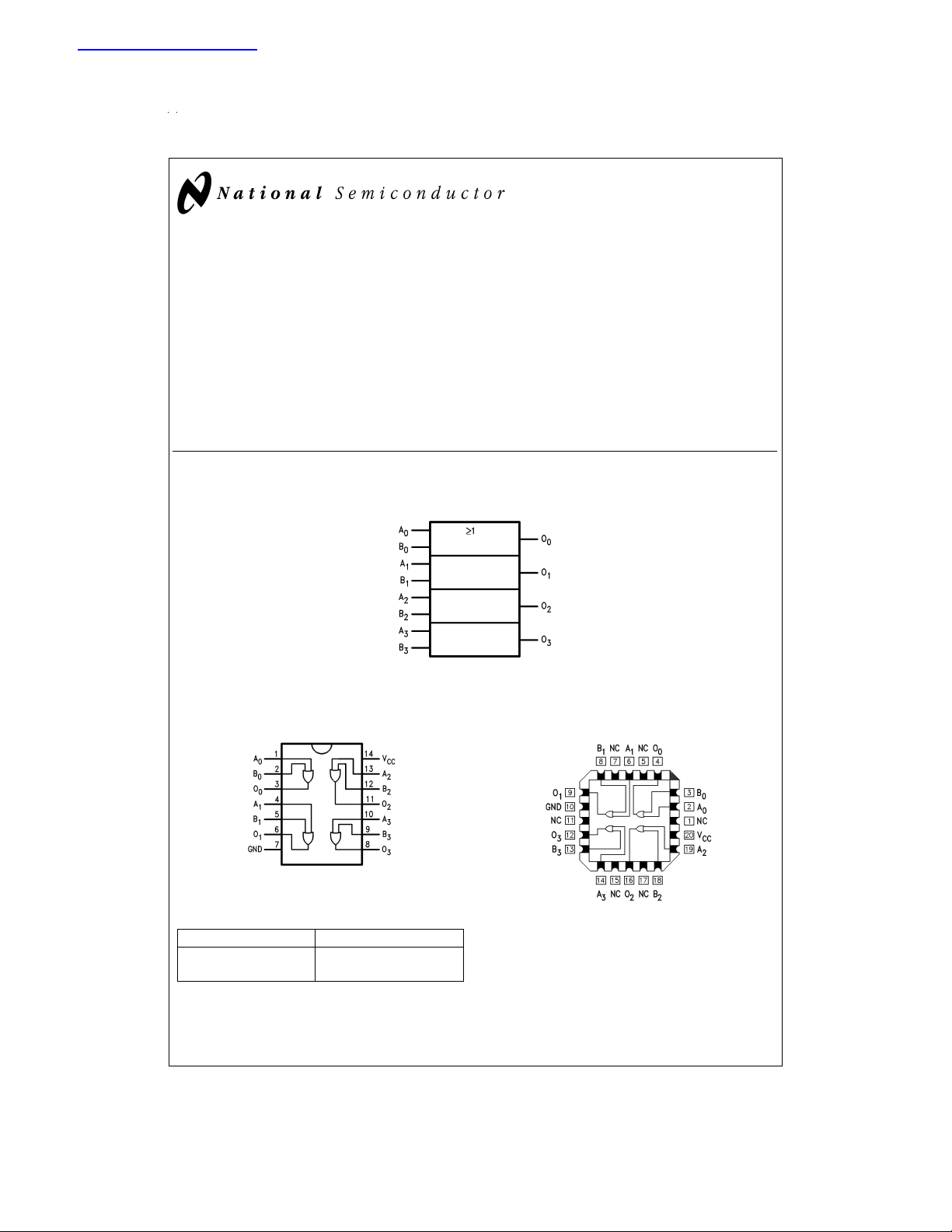
Quiet Series Quad 2-Input OR Gate
General Description
The ’ACTQ32 contains four, 2-input OR gates and utilizes
NSC Quiet Series technology to guarantee quiet output
switching and improved dynamic threshold performance.
FACT Quiet Series
dershoot corrector in addition to a split ground bus for superior ACMOS performance.
Features
n ICCreduced by 50
Logic Symbol
™
features GTO™output control and un-
%
54ACTQ32 Quiet Series Quad 2-Input OR Gate
September 1998
n Guaranteed simultaneous switching noise level and
dynamic threshold performance
n Improved latch-up immunity
n Outputs source/sink 24 mA
n ’ACTQ32 has TTL-compatible inputs
n Standard Microcircuit Drawing (SMD) 5962-8973601
Connection Diagrams
Pin Assignment for DIP and Flatpak
Pin Names Description
A
O
n,Bn
n
Inputs
Outputs
IEEE/IEC
DS100984-1
Pin Assignment for LCC
DS100984-3
DS100984-2
GTO™is a trademark of National Semiconductor Corporation.
™
FACT
and FACT Quiet Series™are trademarks of Fairchild Semiconductor Corporation.
© 1998 National Semiconductor Corporation DS100984 www.national.com
Absolute Maximum Ratings (Note 1)
If Military/Aerospace specified devices are required,
Junction Temperature (T
CDIP 175˚C
please contact the National Semiconductor Sales Office/
Distributors for availability and specifications.
Supply Voltage (V
DC Input Diode Current (I
=
−0.5V −20 mA
V
I
=
V
V
I
CC
DC Input Voltage (V
DC Output Diode Current (I
=
−0.5V −20 mA
V
O
=
V
V
O
CC
DC Output Voltage (V
) −0.5V to +7.0V
CC
)
IK
+ 0.5V +20 mA
) −0.5V to VCC+ 0.5V
I
)
OK
+ 0.5V +20 mA
) −0.5V to VCC+ 0.5V
O
DC Output Source
or Sink Current (I
or Ground Current
DC V
CC
per Output Pin (I
Storage Temperature (T
)
O
or I
CC
)
GND
) −65˚C to +150˚C
STG
±
50 mA
±
50 mA
Recommended Operating
Conditions
Supply Voltage (VCC)
’ACTQ 4.5V to 5.5V
Input Voltage (V
Output Voltage (VO) 0VtoV
Operating Temperature (TA)
54ACTQ −55˚C to +125˚C
Minimum Input Edge Rate (∆V/∆t)
’ACTQ Devices
V
IN
V
CC
Note 1: Absolute maximum ratings are those values beyond which damage
to the device may occur. The databook specifications should be met, without
exception, to ensure that the system design is reliable over its power supply,
temperature, and output/input loading variables. National does not recommend operation of FACT
DC Characteristics for ’ACTQ Family Devices
54ACTQ
Symbol Parameter V
V
IH
Minimum High Level 4.5 2.0 V V
Input Voltage 5.5 2.0 or V
V
IL
Maximum Low Level 4.5 0.8 V V
Input Voltage 5.5 0.8 or V
V
OH
Minimum High Level 4.5 4.4 V I
Output Voltage 5.5 5.4
V
OL
Maximum Low Level 4.5 0.1 V I
Output Voltage 5.5 0.1
I
IN
Maximum Input 5.5
Leakage Current
I
I
I
I
CCT
OLD
OHD
CC
Maximum 5.5 1.6 mA V
I
/Input
CC
Minimum Dynamic 5.5 50 mA V
Output Current (Note 3) 5.5 −50 mA V
Maximum Quiescent 5.5 80.0 µA V
Supply Current or GND (Note 3)
Note 2: All outputs loaded; thresholds on input associated with output under test.
Note 3: Maximum test duration 2.0 ms, one output loaded at a time.
CC
(V) −55˚C to +125˚C
Guaranteed Limits
4.5 3.70 V IOH= −24 mA
5.5 4.70 I
4.5 0.50 V IOL=24mA
5.5 0.50 I
)
J
) 0VtoV
I
from 0.8V to 2.0V
@
4.5V, 5.5V 125 mV/ns
™
circuits outside databook specifications.
=
T
A
Units Conditions
=
0.1V
OUT
− 0.1V
CC
=
0.1V
OUT
− 0.1V
CC
=
−50 µA
OUT
(Note 2)
=
V
or V
V
IN
IL
= −24 mA
OH
=
50 µA
OUT
(Note 2)
=
V
or V
V
IN
IL
=24mA
OL
±
1.0 µA V
I
I
OLD
OHD
IN
=
=
V
CC
V
CC
=
=
=
V
CC
, GND
1.65V Max
3.85V Min
CC
CC
IH
IH
− 2.1V
www.national.com 2
 Loading...