

National Semiconductor 54ACQ240 Technical data
查询54ACQ240供应商查询54ACQ240供应商
54ACQ240
February 1999
54ACQ240•54ACTQ240
Quiet Series Octal Buffer/Line Driver with TRI-STATE
Outputs
General Description
The ’ACQ/’ACTQ240 is an inverting octal buffer and line
driver designed to be employed as a memory address driver,
clock driver and bus oriented transmitter or receiver which
provides improved PC board density. The ’ACQ/’ACTQ utilizes NSC Quiet Series technology to guaranteequiet output
switching and improve dynamic threshold performance.
FACT Quiet Series
dershoot corrector in addition to a split ground bus for superior performance.
™
features GTO™output control and un-
Features
n ICCand IOZreduced by 50
%
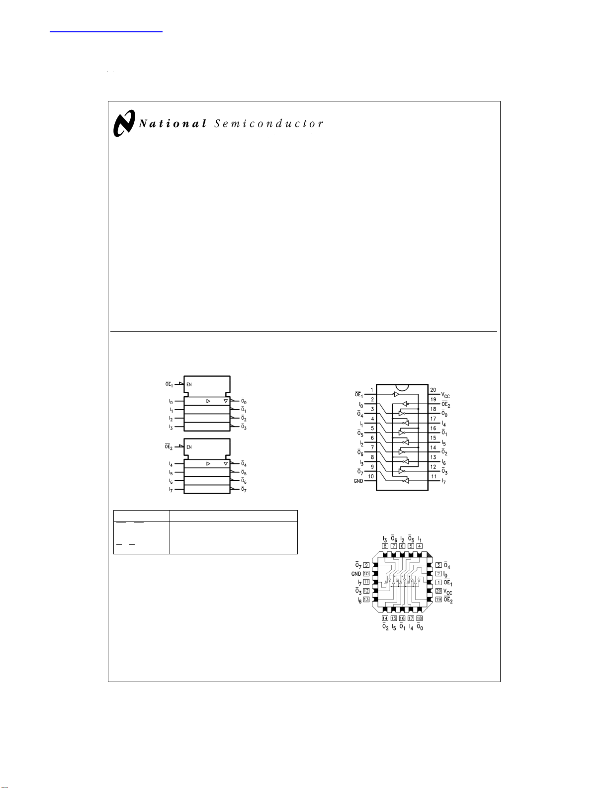
Logic Symbol
IEEE/IEC
n Guaranteed simultaneous switching noise level and
dynamic threshold performance
n Improved latch-up immunity
n Inverting TRI-STATE outputs drive bus lines or buffer
memory address registers
n Outputs source/sink 24 mA
n Faster prop delays than the standard ’ACT240
n 4 kV minimum ESD immunity
n Standard Microcircuit Drawing (SMD)
’ACTQ240: 5962-92184
Connection Diagrams
Pin Assignment
for DIP and Flatpak
®
54ACTQ240 Quiet Series Octal Buffer/Line Driver with TRI-STATE Outputs
•
DS100235-1
Pin Names Description
OE
,OE
1
2
I
0–I7
O
0–O7
GTO™is a trademark of National Semiconductor Corporation.
®
TRI-STATE
is a registered trademark of National Semiconductor Corporation.
®
FACT
is a registered trademark of Fairchild Semiconductor Corporation.
FACT Quiet Series
© 1999 National Semiconductor Corporation DS100235 www.national.com
TRI-STATE Output Enable Inputs
Inputs
Outputs
™
is a trademark of Fairchild Semiconductor Corporation.
Pin Assignment
for LCC
DS100235-2
DS100235-3
Truth Tables
Inputs Outputs
OE
1
LL H
LH L
HX Z
OE
2
LL H
LH L
HX Z
=
H
HIGH Voltage Level
L=LOW Voltage Level
X=Immaterial
Z=High Impedance
I
n
(Pins 12, 14, 16, 18)
Inputs Outputs
I
n
(Pins 3, 5, 7, 9)
www.national.com 2
Absolute Maximum Ratings (Note 1)
If Military/Aerospace specified devices are required,
please contact the National Semiconductor Sales Office/
Distributors for availability and specifications.
Supply Voltage (V
DC Input Diode Current (I
=
−0.5V −20 mA
V
I
=
V
V
I
CC
DC Input Voltage (V
DC Output Diode Current (I
=
−0.5V −20 mA
V
O
=
V
V
O
CC
DC Output Voltage (V
DC Output Source
or Sink Current (I
or Ground Current
DC V
CC
per Output Pin (I
Storage Temperature (T
DC Latch-Up Source or
Sink Current
Junction Temperature (T
CDIP 175˚C
) −0.5V to +7.0V
CC
)
IK
+ 0.5V +20 mA
) −0.5V to VCC+ 0.5V
I
)
OK
+ 0.5V +20 mA
) −0.5V to VCC+ 0.5V
O
)
O
or I
CC
)
GND
) −65˚C to +150˚C
STG
)
J
±
50 mA
±
50 mA
±
300 mA
Recommended Operating
Conditions
Supply Voltage (VCC)
’ACQ 2.0V to 6.0V
’ACTQ 4.5V to 5.5V
Input Voltage (V
Output Voltage (VO) 0VtoV
Operating Temperature (TA)
54ACQ/ACTQ −55˚C to +125˚C
Minimum Input Edge Rate ∆V/∆t
’ACQ Devices
V
IN
V
CC
Minimum Input Edge Rate ∆V/∆t
’ACTQ Devices
V
IN
V
CC
Note 1: Absolute maximum ratings are those values beyond which damage
to the device may occur. The databook specifications should be met, without
exception, to ensure that the system design is reliable over its power supply,
temperature, and output/input loading variables. National does not recommend operation of FACT
Note 2: All commercial packaging is not recommended for applications requiring greater than 2000 temperature cycles from −40˚C to +125˚C.
DC Characteristics for ’ACQ Family Devices
54ACQ
Symbol Parameter V
V
IH
Minimum High Level 3.0 2.1 V
Input Voltage 4.5 3.15 V or V
V
IL
Maximum Low Level 3.0 0.9 V
Input Voltage 4.5 1.35 V or V
V
OH
Minimum High Level 3.0 2.9 I
Output Voltage 4.5 4.4 V
V
OL
Maximum Low Level 3.0 0.1 I
Output Voltage 4.5 0.1 V
I
IN
Maximum Input 5.5
Leakage Current (Note 5)
CC
(V) −55˚C to +125˚C
5.5 3.85
5.5 1.65
5.5 5.4
3.0 2.4 IOH= −12 mA
4.5 3.7 V I
5.5 4.7 I
5.5 0.1
3.0 0.50 IOL=12mA
4.5 0.50 V I
5.5 0.50 I
T
A
Guaranteed Limits
±
1.0 µA V
) 0VtoV
I
from 30%to 70%of V
@
3.0V, 4.5V, 5.5V 125 mV/ns
CC
from 0.8V to 2.0V
@
4.5V, 5.5V 125 mV/ns
®
circuits outside databook specifications.
=
Units Conditions
=
0.1V
OUT
− 0.1V
CC
=
0.1V
OUT
− 0.1V
CC
=
−50 µA
OUT
(Note 3)
=
V
IN
= −24 mA
OH
= −24 mA
OH
OUT
V
=
or V
IL
50 µA
(Note 3)
=
V
IN
=24mA
OL
=24mA
OL
=
I
or V
V
IL
, GND
V
CC
CC
CC
IH
IH
www.national.com3
 Loading...