查询54283供应商
54283/DM74283
4-Bit Binary Full Adder (with Fast Carry)
General Description
The ’283 high speed 4-bit binary full adders with internal
carry lookahead accept two 4-bit binary words (A0 –A3, B0 –
B3) and a Carry input (C0). They generate the binary Sum
outputs (S0 –S3) and the Carry output (C4) from the most
significant bit. They operate with either active HIGH or active LOW operands (positive or negative logic).
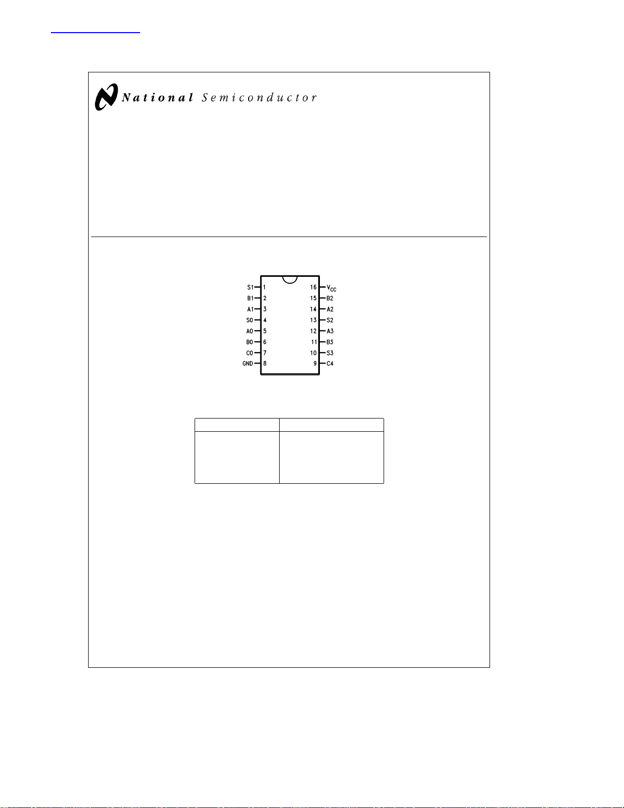
Connection Diagram
54283/DM74283 4-Bit Binary Full Adder (with Fast Carry)
June 1989
Dual-In-Line Package
Order Number 54283DMQB, 54283FMQB or DM74283N
See NS Package Number J16A, N16E or W16A
Pin Names Description
A0–A3 A Operand Inputs
B0–B3 B Operand Inputs
C0 Carry Input
S0–S3 Sum Outputs
C4 Carry Output
TL/F/9786– 1
C
1995 National Semiconductor Corporation RRD-B30M115/Printed in U. S. A.
TL/F/9786

Absolute Maximum Ratings (Note)
The ‘‘Absolute Maximum Ratings’’ are those values
If Military/Aerospace specified devices are required,
please contact the National Semiconductor Sales
Office/Distributors for availability and specifications.
Supply Voltage 7V
Input Voltage 5.5V
Operating Free Air Temperature Range
54
DM74 0
Storage Temperature Range
b
55§Ctoa125§C
Ctoa70§C
§
b
65§Ctoa150§C
Note:
beyond which the safety of the device cannot be guaranteed. The device should not be operated at these limits. The
parametric values defined in the ‘‘Electrical Characteristics’’
table are not guaranteed at the absolute maximum ratings.
The ‘‘Recommended Operating Conditions’’ table will define
the conditions for actual device operation.
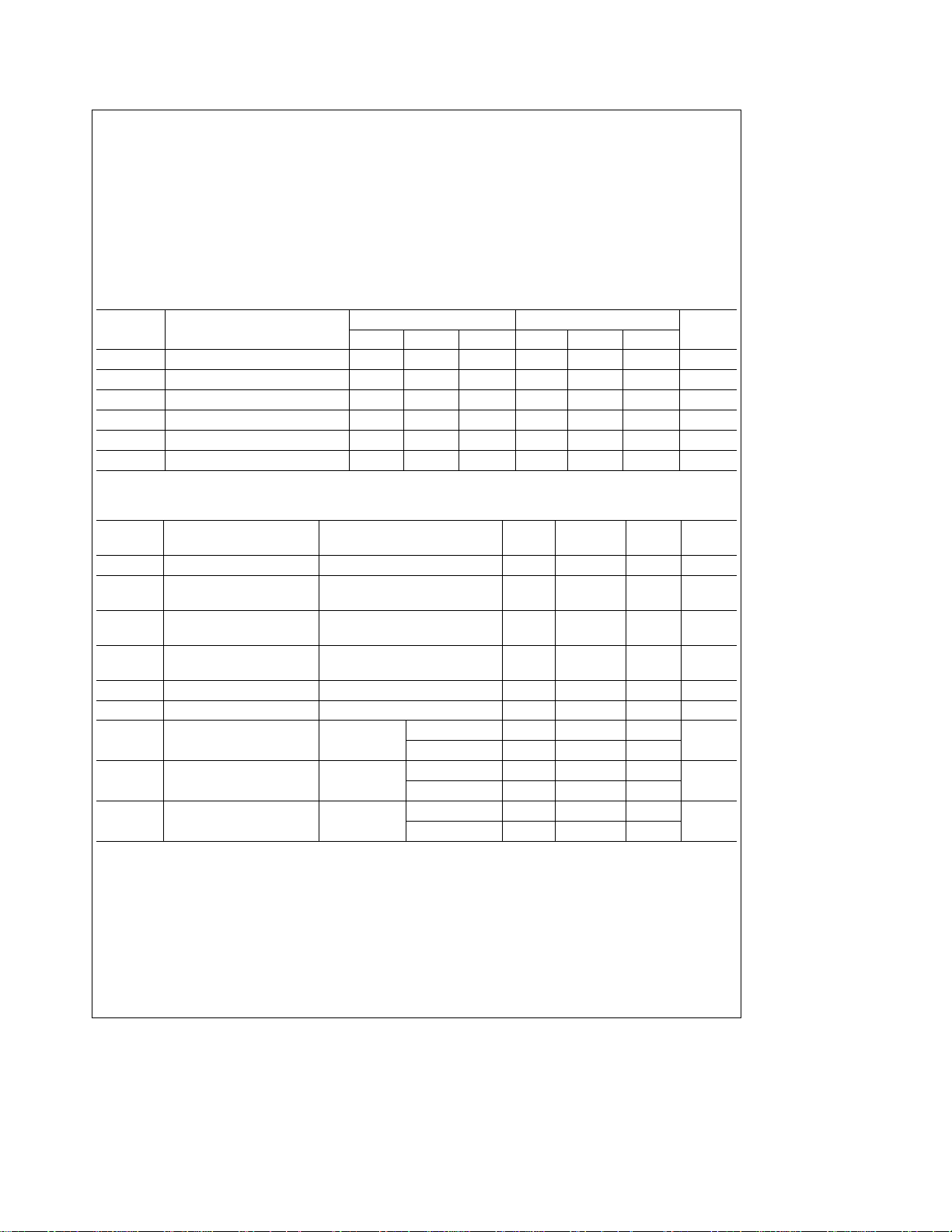
Recommended Operating Conditions
Symbol Parameter
V
CC
V
IH
V
IL
I
OH
I
OL
T
A
Supply Voltage 4.5 5 5.5 4.75 5 5.25 V
High Level Input Voltage 2 2 V
Low Level Input Voltage 0.8 0.8 V
High Level Output Current
Low Level Output Current 16 16 mA
Free Air Operating Temperature
Min Nom Max Min Nom Max
b
54283 DM74283
b
0.4
55 125 0 70
Electrical Characteristics
Over recommended operating free air temperature range (unless otherwise noted)
Symbol Parameter Conditions Min
e
V
I
V
OH
V
OL
I
I
I
IH
I
IL
I
OS
I
OS
I
CCH
Note 1: All typicals are at V
Note 2: Not more than one output should be shorted at a time.
Input Clamp Voltage V
High Level Output Voltage V
V
Low Level Output Voltage V
V
Input Current@Max V
Input Voltage
High Level Input Current V
Low Level Input Current V
Short Circuit V
Output Current at S
n
(Note 2)
Short Circuit V
Output Current at C4 (Note 2)
Supply Current with V
Outputs High
e
e
5V, T
CC
25§C.
A
CC
CC
IL
CC
IH
CC
CC
CC
CC
CC
CC
e
e
eb
Min, I
e
Min, I
Max
e
Min, I
Min
e
Max, V
e
Max, V
e
Max, V
e
Max 54
e
Max 54
e
Max 54 99
12 mA
I
e
Max
OH
e
Max
OL
e
5.5V
I
e
2.4V 40 mA
I
e
0.4V
I
DM74
DM74
2.4 3.4 V
b
b
b
b
DM74 110
Units
b
0.4 mA
C
§
Typ
(Note 1)
Max Units
b
1.5 V
0.2 0.4 V
1mA
b
1.6 mA
20
20
20
18
b
55
b
55
b
70
b
70
mA
mA
mA
2
 Loading...