查询54279供应商
54279/DM74279 Quad Set-Reset Latch
General Description
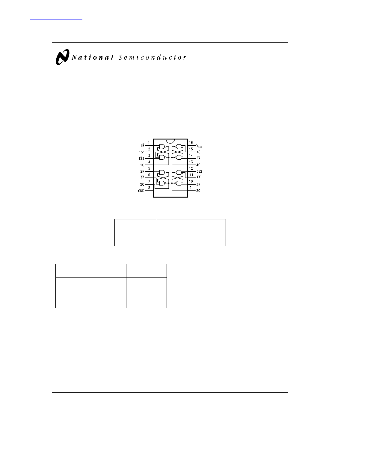
This device contains four independent set-reset type flipflops with one Q output each.
Connection Diagram
54279/DM74279 Quad Set-Reset Latch
June 1989
Dual-In-Line Package
Order Number 54279DMQB, 54279FMQB or DM74279N
NS Package Number J16A, N16E or W16A
Pin Names Description
R
n
S
n
Q Outputs
Truth Table
S
LLL h
LXH H
XLH H
HHL L
H H H No Change
HeHIGH Voltage Level
e
L
LOW Voltage Level
e
X
Immaterial
e
h
The output is HIGH as long as S1orS2 is LOW. If all inputs go HIGH
simultaneously, the output state is indeterminate; otherwise, it follows the
Truth Table.
Inputs Output
1S2R Q
TL/F/9785– 1
Reset Inputs (Active Low)
Set Inputs (Active Low)
C
1995 National Semiconductor Corporation RRD-B30M115/Printed in U. S. A.
TL/F/9785

Absolute Maximum Ratings (Note)
The ‘‘Absolute Maximum Ratings’’ are those values
If Military/Aerospace specified devices are required,
please contact the National Semiconductor Sales
Office/Distributors for availability and specifications.
Supply Voltage 7V
Input Voltage 5.5V
Operating Free Air Temperature Range
54
DM74 0
Storage Temperature Range
b
55§Ctoa125§C
Ctoa70§C
§
b
65§Ctoa150§C
Note:
beyond which the safety of the device cannot be guaranteed. The device should not be operated at these limits. The
parametric values defined in the ‘‘Electrical Characteristics’’
table are not guaranteed at the absolute maximum ratings.
The ‘‘Recommended Operating Conditions’’ table will define
the conditions for actual device operation.
Recommended Operating Conditions
Symbol Parameter
V
CC
V
IH
V
IL
I
OH
I
OL
T
A
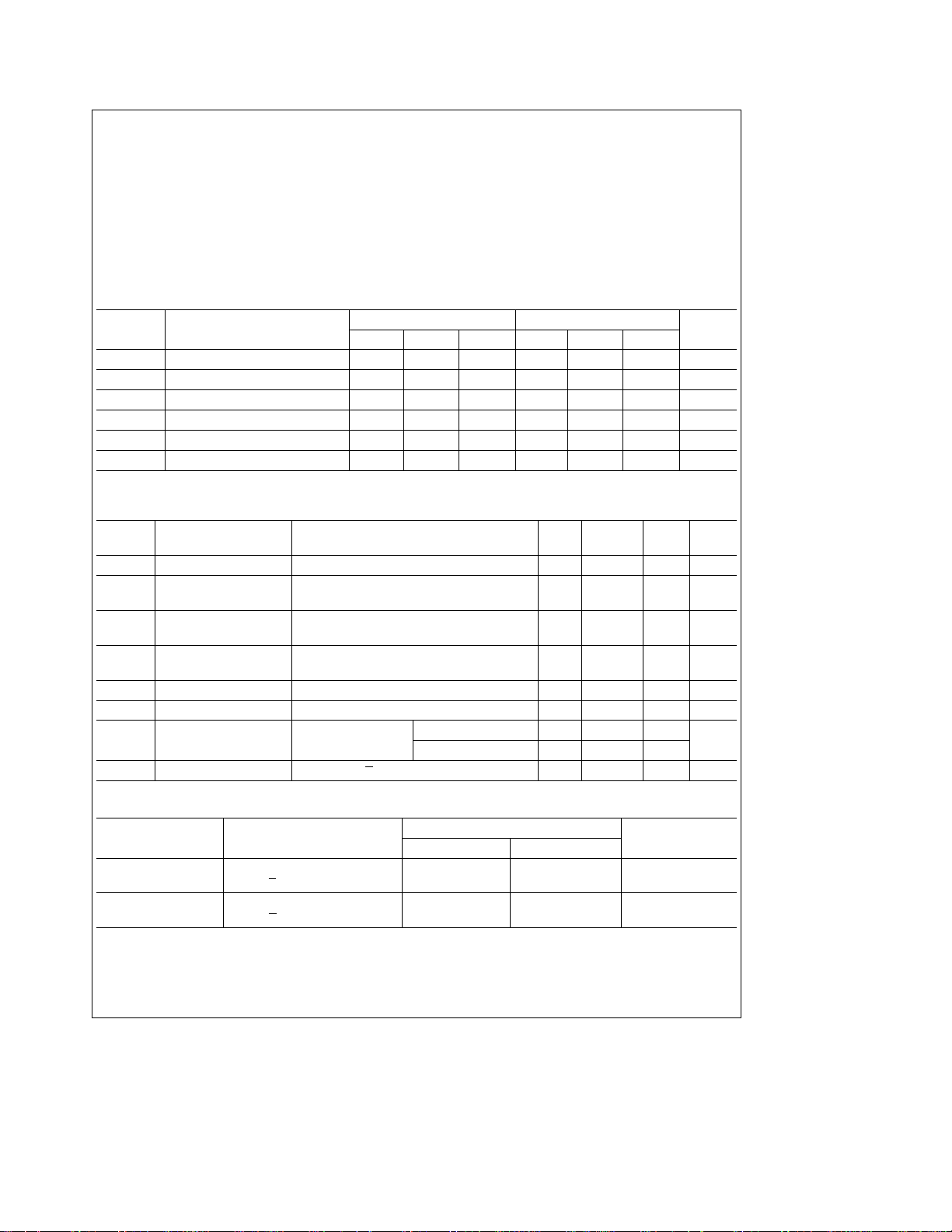
Supply Voltage 4.5 5 5.5 4.75 5 5.25 V
High Level Input Voltage 2 2 V
Low Level Input Voltage 0.8 0.8 V
High Level Output Current
Low Level Output Current 16 16 mA
Free Air Operating Temperature
Min Nom Max Min Nom Max
b
54279 DM74279
b
0.8
55 125 0 70
Electrical Characteristics
over Recommended Operating Free Air Temperature Range (Unless Otherwise Noted)
Symbol Parameter Conditions Min
e
V
I
V
OH
V
OL
I
I
I
IH
I
IL
I
OS
I
CC
Input Clamp Voltage V
High Level V
Output Voltage V
Low Level V
Output Voltage V
Input Current@Max V
Input Voltage
High Level Input Current V
Low Level Input Current V
Short Circuit V
Output Current (Note 2)
Supply Current V
CC
CC
IL
CC
IH
CC
CC
CC
CC
CC
e
e
eb
Min, I
e
Min, I
Max
e
Min, I
Min
e
Max, V
e
Max, V
e
Max, V
e
Max 54
e
Max, Re0V 30 mA
12 mA
I
e
Max,
OH
e
Max,
OL
e
5.5V
I
e
2.4V 40 mA
I
e
0.4V
I
DM74
2.4 3.4 V
b
b
Typ
(Note 1)
0.2 0.4 V
20
18
b
0.8 mA
Max Units
b
1.5 V
1mA
b
1.6 mA
b
55
b
57
Units
C
§
mA
Switching Characteristics
Symbol Parameter
t
PLH
t
PHL
t
PHL
Note 1: All typicals are at V
Note 2: Not more than one output should be shorted at a time.
CC
Propagation Delay 22
S to Q 15
Propagation Delay
R
5V, T
to Q
e
25§C.
A
e
54/DM74
Min Max
2
Units
ns
27 ns
 Loading...