

查询54191供应商
54191/DM54191/DM74191 Synchronous Up/Down
4-Bit Binary Counter with Mode Control
General Description
This circuit is a synchronous, reversible, up/down counter.
The 191 is a 4-bit binary counter. Synchronous operation is
provided by having all flip-flops clocked simultaneously so
that the outputs change simultaneously when so instructed
by the steering logic. This mode of operation eliminates the
output counting spikes normally associated with asynchronous (ripple clock) counters.
The outputs of the four master-slave flip-flops are triggered
on a low-to-high level transition of the clock input, if the
enable input is low. A high at the enable input inhibits counting. Level changes at either the enable input or the down/
up input should be made only when the clock input is high.
The direction of the count is determined by the level of the
down/up input. When low, the counter counts up and when
high, it counts down.
This counter is fully programmable; that is, the outputs may
be preset to either level by placing a low on the load input
and entering the desired data at the data inputs. The output
will change independent of the level of the clock input. This
feature allows the counters to be used as modulo-N dividers
by simply modifying the count length with the preset inputs.
The clock, down/up, and load inputs are buffered to lower
the drive requirement; which significantly reduces the number of clock drivers, etc., required for long parallel words.
June 1989
Two outputs have been made available to perform the cascading function: ripple clock and maximum/minimum count.
The latter output produces a high-level output pulse with a
duration approximately equal to one complete cycle of the
clock when the counter overflows or underflows. The ripple
clock output produces a low-level output pulse equal in
width to the low-level portion of the clock input when an
overflow or underflow condition exists. The counters can be
easily cascaded by feeding the ripple clock output to the
enable input of the succeeding counter if parallel clocking is
used, or to the clock input if parallel enabling is used. The
maximum/minimum count output can be used to accomplish look-ahead for high-speed operation.
Features
Y
Single down/up count control line
Y
Count enable control input
Y
Ripple clock output for cascading
Y
Asynchronously presettable with load control
Y
Parallel outputs
Y
Cascadable for n-bit applications
Y
Alternate Military/Aerospace device (54191) is available. Contact a National Semiconductor Sales Office/
Distributor for specifications.
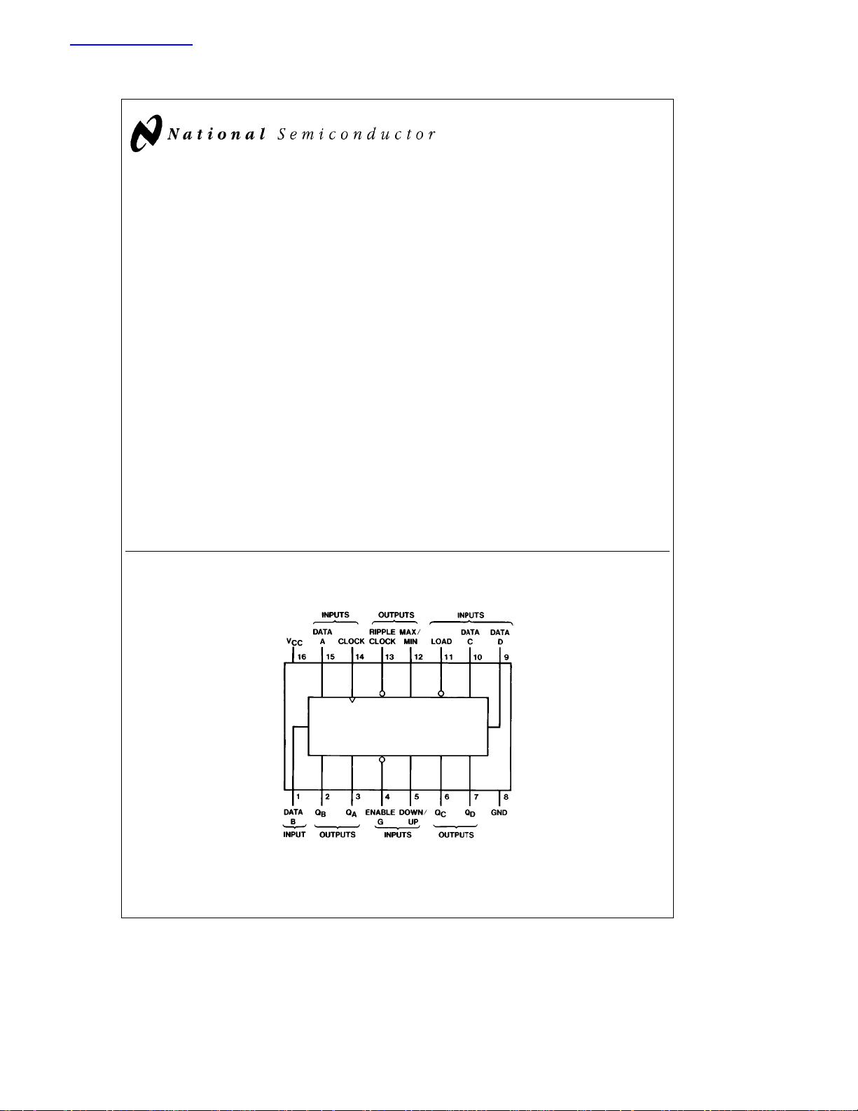
54191/DM54191/DM74191 Synchronous Up/Down 4-Bit Binary Counter with Mode Control
Connection Diagram
Dual-In-Line Package
Order Number 54191DMQB, 54191FMQB,
DM54191J, DM54191W or DM74191N
See NS Package Number J16A, N16E or W16A
C
1995 National Semiconductor Corporation RRD-B30M105/Printed in U. S. A.
TL/F/6562
TL/F/6562– 1
Absolute Maximum Ratings (Note)
If Military/Aerospace specified devices are required,
please contact the National Semiconductor Sales
Office/Distributors for availability and specifications.
Supply Voltage 7V
Input Voltage 5.5V
Operating Free Air Temperature Range
DM54 and 54
DM74 0
Storage Temperature Range
b
55§Ctoa125§C
Ctoa70§C
§
b
65§Ctoa150§C
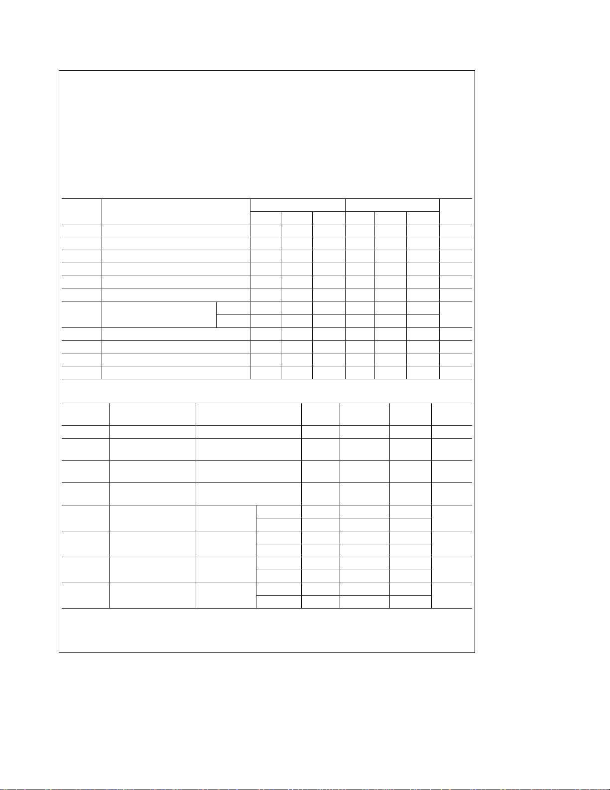
Recommended Operating Conditions
Symbol Parameter
V
V
V
I
OH
I
OL
f
t
t
t
t
T
CC
IH
IL
CLK
W
SU
H
REL
A
Supply Voltage 4.5 5 5.5 4.75 5 5.25 V
High Level Input Voltage 2 2 V
Low Level Input Voltage 0.8 0.8 V
High Level Output Current
Low Level Output Current 16 16 mA
Clock Frequency (Note 4) 0 20 0 20 MHz
Pulse Width Clock 25 25
(Note 4)
Load 35 35
Data Setup Time (Note 4) 28 28 ns
Hold Time (Note 4) 0 0 ns
Load Release Time (Note 4) 30 30 ns
Free Air Operating Temperature
The ‘‘Absolute Maximum Ratings’’ are those values
Note:
beyond which the safety of the device cannot be guaranteed. The device should not be operated at these limits. The
parametric values defined in the ‘‘Electrical Characteristics’’
table are not guaranteed at the absolute maximum ratings.
The ‘‘Recommended Operating Conditions’’ table will define
the conditions for actual device operation.
DM54191 DM74191
Min Nom Max Min Nom Max
b
0.8
b
55 125 0 70
b
Units
0.8 mA
ns
§
C
Electrical Characteristics over recommended operating free air temperature range (unless otherwise noted)
Symbol Parameter Conditions Min
e
V
I
V
OH
V
OL
I
I
I
IH
I
IL
I
OS
I
CC
Note 1: All typicals are at V
Note 2: Not more than one output should be shorted at a time.
Note 3: I
Note 4: T
Input Clamp Voltage V
High Level Output V
Voltage V
Low Level Output V
Voltage V
Input Current@Max V
Input Voltage
High Level Input V
Current V
Low Level Input V
Current V
Short Circuit V
Output Current (Note 2)
Supply Current V
e
e
5V, T
5V.
25§C.
A
CC
is measured with all inputs grounded and all outputs open.
CC
e
A
25§C and V
e
CC
CC
CC
IL
CC
IH
CC
CC
e
I
CC
e
I
CC
CC
(Note 3)
e
e
eb
Min, I
e
Min, I
Max, V
e
Min, I
Min, V
e
Max, V
e
Max Enable 120
2.4V
e
Max Enable
0.4V
e
Max DM54
e
Max DM54 65 99
12 mA
I
e
Max
OH
e
Min
IH
e
Max
OL
e
Max
IL
e
5.5V
I
Others 40
Others
b
DM74
b
DM74 65 105
2
2.4 3.4 V
20
18
Typ
(Note 1)
Max Units
b
1.5 V
0.2 0.4 V
1mA
b
4.8
b
1.6
b
65
b
65
mA
mA
mA
mA

Switching Characteristics at V
Symbol Parameter
f
MAX
t
PLH
t
PHL
t
PLH
t
PHL
t
PLH
t
PHL
t
PLH
t
PHL
t
PLH
t
PHL
t
PLH
t
PHL
t
PLH
t
PHL
t
PLH
t
PHL
Maximum Clock Frequency 20 MHz
Propagation Delay Time Load to
Low to High Level Output Any Q
Propagation Delay Time Load to
High to Low Level Output Any Q
Propagation Delay Time Data to
Low to High Level Output Any Q
Propagation Delay Time Data to
High to Low Level Output Any Q
Propagation Delay Time Clock to
Low to High Level Output Ripple Carry
Propagation Delay Time Clock to
High to Low Level Output Ripple Carry
Propagation Delay Time Clock to
Low to High Level Output Any Q
Propagation Delay Time Clock to
High to Low Level Output Any Q
Propagation Delay Time Clock to
Low to High Level Output Max/Min
Propagation Delay Time Clock to
High to Low Level Output Max/Min
Propagation Delay Time Down/Up to
Low to High Level Output Ripple Carry
Propagation Delay Time Down/Up to
High to Low Level Output Ripple Carry
Propagation Delay Time Down/Up to
Low to High Level Output Max/Min
Propagation Delay Time Down/Up to
High to Low Level Output Max/Min
Propagation Delay Time Enable G to
Low to High Level Output Ripple Carry
Propagation Delay Time Enable G to
High to Low Level Output Ripple Carry
CC
e
5V and T
e
A
From (Input) R
To (Output)
25§C (See Section 1 for Test Waveforms and Output Load)
e
400X,C
L
Min Max
e
15 pF
L
Units
33 ns
70 ns
22 ns
70 ns
20 ns
24 ns
24 ns
36 ns
42 ns
52 ns
45 ns
45 ns
33 ns
33 ns
24 ns
24 ns
3

Logic Diagram
191 Binary Counter
TL/F/6562– 2
4
Pin (16)eVCC, Pin (8)eGND

Timing Diagrams
Typical Load, Count, and Inhibit Sequences
191 Decade Counter
Physical Dimensions inches (millimeters)
TL/F/6562– 3
16-Lead Ceramic Dual-In-Line Package (J)
Order Number 54191DMQB or DM54191J
NS Package Number J16A
5

Physical Dimensions inches (millimeters) (Continued)
16-Lead Molded Dual-In-Line Package (N)
Order Number DM74191N
NS Package Number N16E
16-Lead Ceramic Flat Package (W)
Order Number 54191FMQB or DM54191W
LIFE SUPPORT POLICY
NS Package Number W16A
NATIONAL’S PRODUCTS ARE NOT AUTHORIZED FOR USE AS CRITICAL COMPONENTS IN LIFE SUPPORT
DEVICES OR SYSTEMS WITHOUT THE EXPRESS WRITTEN APPROVAL OF THE PRESIDENT OF NATIONAL
SEMICONDUCTOR CORPORATION. As used herein:
1. Life support devices or systems are devices or 2. A critical component is any component of a life
systems which, (a) are intended for surgical implant support device or system whose failure to perform can
into the body, or (b) support or sustain life, and whose be reasonably expected to cause the failure of the life
failure to perform, when properly used in accordance support device or system, or to affect its safety or
with instructions for use provided in the labeling, can effectiveness.
be reasonably expected to result in a significant injury
to the user.
National Semiconductor National Semiconductor National Semiconductor National Semiconductor
Corporation Europe Hong Kong Ltd. Japan Ltd.
1111 West Bardin Road Fax: (
54191/DM54191/DM74191 Synchronous Up/Down 4-Bit Binary Counter with Mode Control
Arlington, TX 76017 Email: cnjwge@tevm2.nsc.com Ocean Centre, 5 Canton Rd. Fax: 81-043-299-2408
Tel: 1(800) 272-9959 Deutsch Tel: (
Fax: 1(800) 737-7018 English Tel: (
National does not assume any responsibility for use of any circuitry described, no circuit patent licenses are implied and National reserves the right at any time without notice to change said circuitry and specifications.
Fran3ais Tel: (
Italiano Tel: (
a
49) 0-180-530 85 86 13th Floor, Straight Block, Tel: 81-043-299-2309
a
49) 0-180-530 85 85 Tsimshatsui, Kowloon
a
49) 0-180-532 78 32 Hong Kong
a
49) 0-180-532 93 58 Tel: (852) 2737-1600
a
49) 0-180-534 16 80 Fax: (852) 2736-9960
 Loading...