DS90C3202
3.3V 8 MHz to 135 MHz Dual FPD-Link Receiver
DS90C3202 3.3V 8 MHz to 135 MHz Dual FPD-Link Receiver
September 2006
General Description
The DS90C3202 is a 3.3V single/dual FPD-Link 10-bit color
receiver is designed to be used in Liquid Crystal Display
TVs, LCD Monitors, Digital TVs, and Plasma Display Panel
TVs. The DS90C3202 is designed to interface between the
digital video processor and the display device using the
low-power, low-EMI LVDS (Low Voltage Differential Signaling) interface. The DS90C3202 converts up to ten LVDS
data streams back into 70 bits of parallel LVCMOS/LVTTL
data. The receiver can be programmed with rising edge or
falling edge clock. Optional wo-wire serial programming allows fine tuning in development and production environments. With an input clock at 135 MHz, the maximum transmission rate of each LVDS line is 945 Mbps, for an
aggregate throughput rate of 9.45 Gbps (945 Mbytes/s). This
allows the dual 10-bit LVDS Receiver to support resolutions
up to HDTV.
Block Diagram
Features
n Up to 9.45 Gbit/s data throughput
n 8 MHz to 135 MHz input clock support
n Supports up to QXGA panel resolutions
n Supports HDTV panel resolutions and frame rates up to
1920 x 1080p
n LVDS 30-bit, 24-bit or 18-bit color data inputs
n Supports single pixel and dual pixel interfaces
n Supports spread spectrum clocking
n Two-wire serial communication interface
n Programmable clock edge and control strobe select
n Power down mode
n +3.3V supply voltage
n 128-pin TQFP Package
n Compliant to TIA/EIA-644-A-2001 LVDS Standard
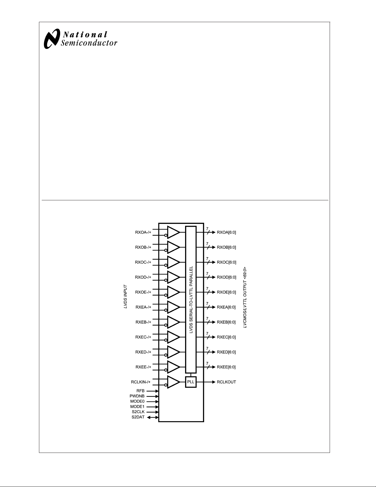
FIGURE 1. Receiver Block Diagram
© 2006 National Semiconductor Corporation DS201471 www.national.com
20147101
Typical Application Diagram
DS90C3202
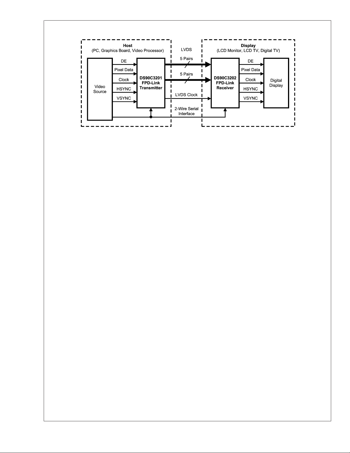
FIGURE 2. LCD Panel Application Diagram
Functional Description
The DS90C3201 and DS90C3202 are a dual 10-bit color
Transmitter and Receiver FPD-Link chipset designed to
transmit data at clocks speeds from 8 to 135 MHz.
DS90C3201 and DS90C3202 are designed to interface between the digital video processor and the display using a
LVDS interface. The DS90C3201 transmitter serializes 2
channels of video data (10-bit each for RGB for each channel, totaling 60 bits) and control signals (HSYNC, VSYNC,
DE and two user-defined signals) along with clock signal to
10 channels of LVDS signals and transmits them. The
DS90C3202 receiver converts 10 channels of LVDS signals
into parallel signals and outputs 2 channels of video data
(10-bit each for RGB for each channel, totaling 60 bits) and
control signals (HSYNC, VSYNC, DE and two user-defined
signals) along with clock signal. The dual high speed LVDS
channels supports single pixel in-single pixel out and dual
pixel in-dual pixel out transmission modes. The FPD-Link
chipset is suitable for a variety of display applications including LCD Monitors, LCD TV, Digital TV, and DLP TV, and
Plasma Display Panels.
Using a true 10-bit color depth system, the 30-bit RGB color
produces over 1.07 billion colors to represent High Definition
(HD) displays in their most natural color, surpassing the
maximum 16.7 million colors achieved by 6/8-bit color conventionally used for large-scale LCD televisions and LCD
monitors.
LVDS RECEIVER
The LVDS Receiver receives input RGB video data and
control signal timing.
20147102
2-WIRE SERIAL COMMUNICATION INTERFACE
Optional Two-Wire serial interface programming allows fine
tuning in development and production environments. The
Two-Wire serial interface provides several capabilities to
reduce EMI and to customize output timing. These capabilities are selectable/programmable via Two-Wire serial interface: Programmable Skew Rates, Progress Turn On Function, Input/Output Channel Control.
PROGRAMMABLE SKEW RATES
Programmable edge rates allow the LVCMOS/LVTTL Data
and Clock outputs to be adjusted for better impedance
matching for noise and EMI reduction. The individual output
drive control registers for Rx data out and Rx clock out are
programmable via Two-Wire serial interface.
PROGRESS TURN ON FUNCTION
Progress Turn On (PTO) function aligns the two output channels of LVCMOS/LVTLL in either a non-skew data format
(simultaneous switching) or a skewed data format (staggered). The skewed format delays the selected channel data
and staggers the outputs. This reduces the number of outputs switching simultaneously, which lowers EMI radiation
and minimizes ground bounce. Feature is controlled via
Two-Wire serial interface.
INPUT/OUTPUT CHANNEL CONTROL
Full independent control for input/output channels can be
disabled to minimize power supply line noise and overall
power dissipation. Feature is configured via Two-Wire serial
interface
SELECTABLE OUTPUT DATA STROBE
The Receiver output data edge strobe can be latched on the
rising or falling edges of clock signal. The dedicated RFB pin
is used to program output strobe select on the rising edge of
RCLK or the falling edge of RCLK.
www.national.com 2
DS90C3202
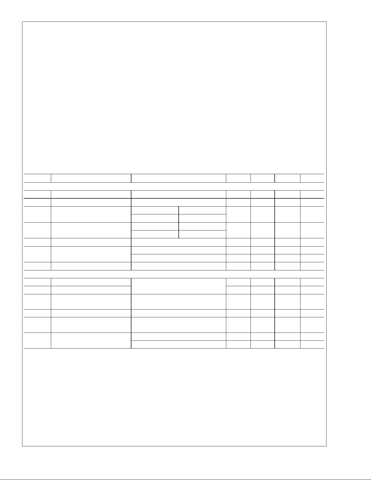
Absolute Maximum Ratings (Note 1)
If Military/Aerospace specified devices are required,
please contact the National Semiconductor Sales Office/
Distributors for availability and specifications.
Supply Voltage (V
LVCMOS/LVTTL Input
Voltage −0.3V to (V
LVCMOS/LVTTL Output
Voltage −0.3V to (VDD+ 0.3V)
LVDS Receiver Input Voltage −0.3V to (V
Junction Temperature +150˚C
Storage Temperature −65˚C to +150˚C
Lead Temperature
(Soldering, 10 sec.) +260˚C
Maximum Package Power Dissipation Capacity
) −0.3V to +4V
DD
+ 0.3V)
DD
+ 0.3V)
DD
@
25˚C
Package Derating: 25.6mW/˚C above +25˚C
ESD Rating:
(HBM, 1.5kΩ, 100pF)
(EIAJ, 0Ω, 200pF)
>
>
2kV
200 V
Recommended Operating Conditions
Min Nom Max Units
Supply Voltage (V
Operating Free Air
Temperature (TA) 0 +25 +70 ˚C
Supply Noise Voltage (V
Receiver Input Range 0 V
Input Clock Frequency (f) 8 135 MHz
) 3.15 3.3 3.6 V
DD
P-P
)
±
100 mV
DD
p-p
V
128 TQFP Package: 1.4W
Electrical Characteristics
Over recommended operating supply and temperature ranges unless otherwise specified.
Symbol Parameter Conditions Min Typ Max Units
CMOS/TTL DC SPECIFICATIONS (Rx outputs, control inputs and outputs)
V
IH
V
IL
V
OH
V
OL
V
CL
I
IN
I
OS
LVDS RECEIVER DC SPECIFICATIONS
V
TH
V
TL
V
IN
| Differential Input Voltage 0.200 0.600 V
|V
ID
V
CM
I
IN
High Level Input Voltage 2.0 V
DD
Low Level Input Voltage 0 0.8 V
High Level Output Voltage Rx clock out IOH=−4mA 2.4 V
Rx data out I
=−2mA
OH
Low Level Output Voltage Rx clock out IOL=+4mA 0.4 V
Rx data out I
=+2mA
OL
Input Clamp Voltage ICL= −18 mA −0.8 −1.5 V
Input Current VIN=V
V
= 0V −10 µA
IN
Output Short Circuit Current V
= 0V −120 mA
OUT
DD
+10 µA
Differential Input High Threshold VCM= +1.2V +100 mV
Differential Input Low Threshold −100 mV
Input Voltage Range
0V
DD
(Single-ended)
Differential Common Mode
0.2 1.2 VDD−0.1 V
Voltage
Input Current VIN= +2.4V, VDD= 3.6V
V
= 0V, VDD= 3.6V
IN
±
10 µA
±
10 µA
V
V
www.national.com3
Electrical Characteristics (Continued)
Over recommended operating supply and temperature ranges unless otherwise specified.
Symbol Parameter Conditions Min Typ Max Units
DS90C3202
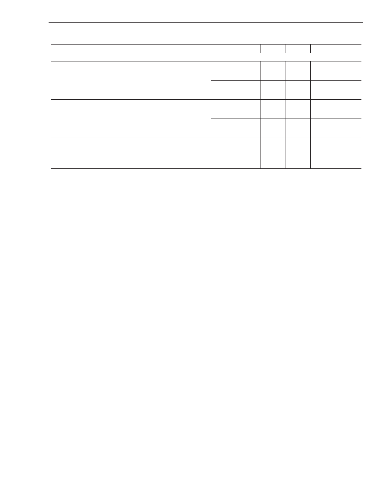
RECEIVER SUPPLY CURRENT
ICCRW Receiver Supply Current
Worst Case
(Figures 2, 4)
ICCRG Receiver Supply Current
Incremental Test Pattern
(Figures 3, 4)
ICCRZ Receiver Supply Current
Power Down
Note 1: “Absolute Maximum Ratings” are those values beyond which the safety of the device cannot be guaranteed. They are not meant to imply that the device
should be operated at these limits. The tables of “Electrical Characteristics” specify conditions for device operation.
Note 2: Typical values are given for V
Note 3: Current into device pins is defined as positive. Current out of device pins is defined as negative. Voltages are referenced to ground unless otherwise
specified.
Note 4: The worst case test pattern produces a maximum toggling of digital circuits, LVDS I/O and LVCMOS/LVTTL I/O.
Note 5: The incremental test pattern tests device power consumption for a “typical” LCD display pattern.
Note 6: Figures 2, 3 show a falling edge data strobe (RCLK OUT).
Note 7: Figure 8 show a rising edge data strobe (RCLK OUT).
= 3.3V and TA= +25˚C.
DD
= 8 pF,
C
L
f = 8 MHz 65 130 mA
Worst Case
Pattern
Default Register
f = 135 MHz 375 550 mA
Settings
C
L
= 8 pF,
f = 8 MHz 55 120 mA
Worst Case
Pattern
Default Register
f = 135 MHz 245 400 mA
Settings
PDWNB = Low
Receiver Outputs stay low
during Powerdown mode.
Default Register Settings
2mA
www.national.com 4
DS90C3202
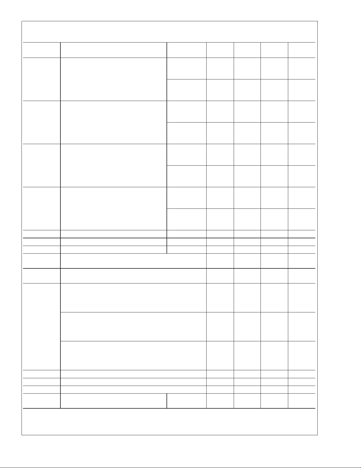
Receiver Switching Characteristics
Over recommended operating supply and temperature ranges unless otherwise specified.
Symbol Parameter Condition/
Reference
CLHT LVCMOS/LVTTL Low-to-High Transition
Time, C
= 8pF, (Figure 5) (Note 8)
L
Rx clock out 1.45 2.10 ns
Register addr 28d/1ch,
bit [2] (RCLK)=0b (Default),
Rx data out 2.40 3.50 ns
bit [1] (RXE) =0b (Default),
bit [0] (RXO) =0b (Default)
CHLT LVCMOS/LVTTL High-to-Low Transition
Time, C
= 8pF, (Figure 5) (Note 8)
L
Rx clock out 1.35 2.20 ns
Register addr 28d/1ch,
bit [2] (RCLK)=0b (Default),
Rx data out 2.40 3.60 ns
bit [1] (RXE) =0b (Default),
bit [0] (RXO) =0b (Default)
CLHT
Programmable
adjustment
LVCMOS/LVTTL Low-to-High Transition
Time, C
= 8pF, (Figure 5) (Note 8)
L
Register addr 28d/1ch,
bit [2] (RCLK)=1b (Default),
Rx clock out 2.45 ns
Rx data out 3.40 ns
bit [1] (RXE) =1b (Default),
bit [0] (RXO) =1b (Default)
CHLT
Programmable
adjustment
LVCMOS/LVTTL High-to-Low Transition
Time, C
= 8pF, (Figure 5) (Note 8)
L
Register addr 28d/1ch,
bit [2] (RCLK)=0b (Default),
Rx clock out 2.35 ns
Rx data out 3.40 ns
bit [1] (RXE) =0b (Default),
bit [0] (RXO) =0b (Default)
RCOP RCLK OUT Period (Figures 11, 12) (Note 8) 8–135 MHz 7.4 T 125 ns
RCOH RCLK OUT High Time (Figures 11, 12) Rx clock out 0.4T 0.5T 0.6T ns
RCOL RCLK OUT Low Time (Figures 11, 12) Rx clock out 0.4T 0.5T 0.6T ns
RSRC RxOUT Setup to RCLK OUT (Figures 11, 12) (Notes 8, 9)
Register addr 29d/1dh [2:1]= 00b (Default)
RHRC RxOUT Hold to RCLK OUT (Figures 11, 12) (Notes 8, 9)
Register addr 29d/1dh [2:1]= 00b (Default)
RSRC/RHRC
Programmable
Adjustment
Register addr 29d/1dh [2:1] = 01b, (Figures 13, 14)
(Notes 2, 10)
RSRC increased from default by 1UI
RHRC decreased from default by 1UI
Register addr 29d/1dh [2:1] = 10b, (Figures 13, 14)
(Notes 2, 10)
RSRC decreased from default by 1UI
RHRC increased from default by 1UI
Register addr 29d/1dh [2:1] = 11b, (Figures 13, 14)
(Notes 2, 10)
RSRC increased from default by 2UI
RHRC decreased from default by 2UI
RPLLS Receiver Phase Lock Loop Set (Figure 6)10ms
RPDD Receiver Powerdown Delay (Figure 7) 100 ns
RPDL Receiver Propagation Delay — Latency (Figure 8) 4*RCLK ns
RITOL Receiver Input Tolerance
(Figures 10, 16) (Notes 8, 10)
Note 8: Specification is guaranteed by characterization.
Note 9: A Clock Unit Symbol (T) is defined as 1/ (Line rate of RCLK). E.g. For Line rate of RCLK at 85MHz, 1 T = 11.76ns
Note 10: A Unit Interval (UI) is defined as 1/7th of an ideal clock period (RCLK/7). E.g. For an 11.76ns clock period (85MHz), 1 UI = 1.68ns
V
CM
V
ID
= 1.25V,
= 350mV
Min Typ Max Units
2.60 0.5T ns
3.60 0.5T ns
+1UI /
ns
-1UI
-1UI /
ns
+1UI
+2UI /
ns
-2UI
0.25 UI
www.national.com5
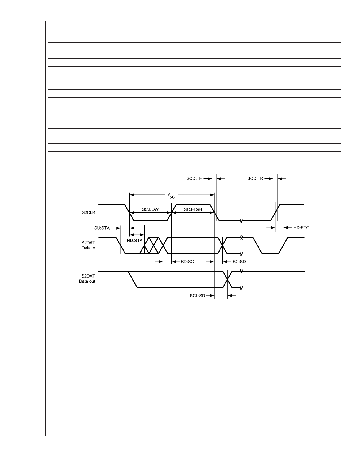
Two-Wire Serial Communication Interface
Over recommended operating supply and temperature ranges unless otherwise specified.
Symbol Parameter Conditions Min Typ Max Units
DS90C3202
f
SC
SC:LOW Clock Low Period R
SC:HIGH Clock High Period R
SCD:TR S2CLK and S2DAT Rise Time R
SCD:TF S2CLK and S2DAT Fall Time R
SU:STA Start Condition Setup Time R
HD:STA Start Condition Hold Time R
HD:STO Stop Condition Hold Time R
SC:SD Clock Falling Edge to Data R
SD:SC Data to Clock Rising Edge R
SCL:SD S2CLK Low to S2DAT Data
S2CLK Clock Frequency 400 kHz
= 4.7KΩ,CL= 50pF 1.5 us
P
= 4.7KΩ,CL= 50pF 0.6 us
P
= 4.7KΩ,CL= 50pF 0.3 us
P
= 4.7KΩ,CL= 50pF 0.3 us
P
= 4.7KΩ,CL= 50pF 0.6 us
P
= 4.7KΩ,CL= 50pF 0.6 us
P
= 4.7KΩ,CL= 50pF 0.6 us
P
= 4.7KΩ,CL= 50pF 0 us
P
= 4.7KΩ,CL= 50pF 0.1 us
P
R
= 4.7KΩ,CL= 50pF 0.1 0.9 us
P
Valid
BUF Bus Free Time RP= 4.7KΩ,CL= 50pF 13 us
AC Timing Diagrams
FIGURE 1. Two-Wire Serial Communication Interface Timing Diagram
www.national.com 6
20147122
AC Timing Diagrams (Continued)
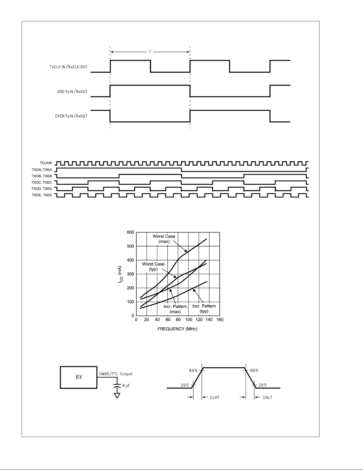
FIGURE 2. “Worst Case” Test Pattern
DS90C3202
20147103
FIGURE 3. Incremental Test Pattern
20147105
FIGURE 4. Typical and Max ICC with Worse Case and Incremental Pattern
20147104
FIGURE 5. LVCMOS/LVTTL Output Load and Transition Times
20147106
www.national.com7
 Loading...