

Page 1

USER MANUAL
NI Digital System Development
Board
The Digital System Development Board (DSDB) is an NI ELVIS add-on board featuring a
Zynq 7020 All Programmable SoC (AP SoC) that was designed by Digilent for National
Instruments. When paired with the NI ELVIS platform, it becomes an ideal lab installation for
classes centered on digital and analog circuits. The DSDB also has the ability to be used as a
standalone Zynq development platform, independent of NI ELVIS.
Contents
Contents .................................................................................................................................... 1
Features..................................................................................................................................... 3
Hardware Components .............................................................................................................5
Power Supplies ......................................................................................................................... 6
I
nput Power Monitoring ................................................................................................... 9
User Power Supplies......................................................................................................... 9
User Power Supplies Monitoring .
Zynq AP SoC Architecture....................................................................................................... 11
Zynq Configuration .................................................................................................................. 15
microSD Boot Mode...........
Quad-SPI Boot
JTAG Boot Mode ..........................
Connecting to NI ELVIS ..........................................................................................................16
SPI Flash................................................................................................................................... 18
DDR3 Memory ......................................................................................................................... 19
USB UART Bridge (Serial Port) .............................................................................................. 20
microSD Slot ............................................................................................................................ 20
USB HID Host.......................................................................................................................... 21
HID Controller.......................................................................................................................... 21
Keyboard .................................................................................................................................. 22
Mouse ....................................................................................................................................... 24
Ethernet..................................................................................................................................... 25
OLED........................................................................................................................................ 26
VGA Port.................................................................................................................................. 29
VGA System Timing ................................................................................................................ 29
HDMI Source/Sink Port ...........................................................................................................33
Touchscreen Display ................................................................................................................ 34
LCD Display...
Capacitive Touchscreen....
Mode ....................................................................................................... 16
..................................................................................................................34
................................................................................................ 36
.................................................................................... 10
.............................................................................................. 16
................................................................................... 16
Page 2

Clock Sources ........................................................................................................................... 39
Basic I/O ................................................................................................................................... 39
Seven-Segment Display ............................................................................................................ 40
Audio ........................................................................................................................................ 42
Reset Sources ............................................................................................................................43
Power-on Reset .
Program Push B
Processor Sub
................................................................................................................43
utton Switch............................................................................................44
system Reset...............................................................................................44
User IO Protection .................................................................................................................... 44
Pmod Connectors ......................................................................................................................44
Stan
dard Pmod..................................................................................................................45
MIO Pmod ..............
..........................................................................................................45
MXP Connector ........................................................................................................................46
Breadboards .............................................................................................................................. 47
NI ELVIS Analog Breadboard .
FPGA Digital IO Breadboard ....................................................................
Power
Breadboard.............................................................................................................48
........................................................................................48
.......................48
DSDB Programming Guide ...................................................................................................... 48
Programming in LabVIEW FPGA ..
Pr
ogramming in Multisim.................................................................................................53
.................................................................................48
Installation and Setup................................................................................................................ 62
Wh
at You Need to Get Started .........................................................................................62
Installation and
Setup Instructions....................................................................................63
2 | ni.com | NI Digital System Development Board User Manual
Page 3
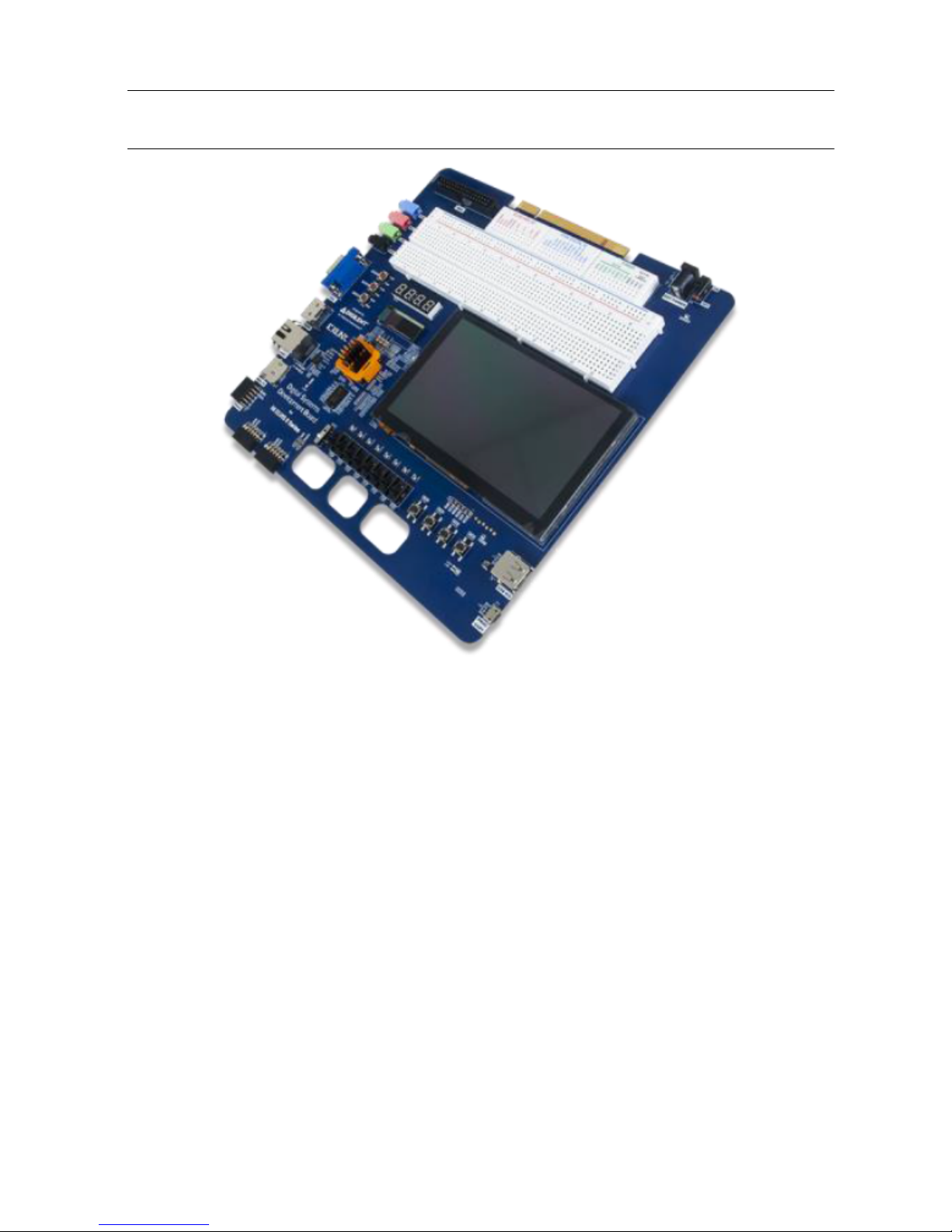
Features
Figure 1. The Digital System Development Board
The DSDB includes the following features:
ZYNQ XC7Z020-1CLG484C
• 650 Mhz dual-core Cortex-A9 processor
• DDR3 memory controller with 8 DMA channels
• High-bandwidth peripheral controllers: 1G Ethernet, SDIO
• Low-bandwidth peripheral controller: SPI, UART, CAN, I2C
• On-chip analog-to-digital converter (XADC) Programmed using JTAG, Quad-SPI Flash, or
microSD
•
Reprogrammable logic equivalent to Artix-7 FPGA
• 13,300 logic slices, each with four 6-input LUTs and eight flip-flops
• 560 KB of fast block RAM
• Four clock management tiles, each with a phase-locked loop (PLL) and mixed-mode
clock manager (MMCM)
• 220 DSP slices
• Internal clock speeds exceeding 450 MHz
NI Digital System Development Board User Manual | © National Instruments | 3
Page 4

System Features
• 512 MB DDR3 with a 32-bit bus @ 1050 MHz
• 16 MB quad-SPI flash
• microSD socket for additional storage
• USB-JTAG programming circuitry
• Current and voltage monitoring on expansion connectors
• Powered from the NI ELVIS connector or 5 V barrel jack input
System Connectivity
• 16-bit VGA output
• Dual-role (source/sink) HDMI port
• NI ELVIS add-on connector
• 24-bit audio codec with headphone, line out, line in, and microphone jacks
• 10/100/1000 Mbps ethernet
• USB-UART bridge
Interaction and Sensory Devices
• 800 × 480 5-in. LCD display with capacitive touchscreen
• 128 × 32 monochrome OLED Display
• Four-digit 7-segment display
• USB HID connector for mice and keyboards
• Eight FPGA-connected LEDs
• One processor-connected LED
• Four push buttons
• Eight slide switches
Expansion Connectors
• MXP Connector
• Breadboard with analog I/O from NI ELVIS and digital I/O from Zynq
• Two Pmod connectors with eight FPGA I/O each
• One Pmod connector with eight Processor I/O
The DSDB is compatible with Xilinx’s new high-performance Vivado Design Suite as well as
the ISE/EDK toolset. These toolsets meld FPGA logic design with embedded ARM software
development into an easy to use, intuitive design flow. They can be used for designing systems
of any complexity, from a complete operating system running multiple server applications in
tandem, down to a simple bare-metal program that controls some LEDs.
4 | ni.com | NI Digital System Development Board User Manual
Page 5
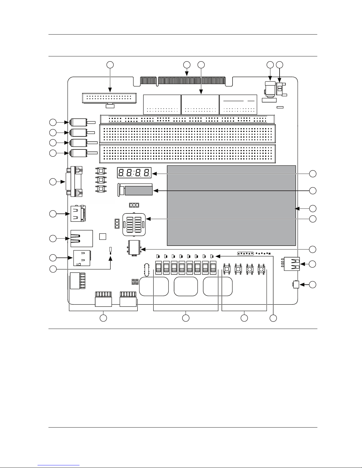
Hardware Components
NI ELVIS II Series
Figure 2. The NI Digital System Development Board
11
ELVIS ANALOG
A12
A11
A12
A11
++–
–+–
++–
MXP
+–
9
8
7
6
5
LINE IN
MIC IN
LINE OUT
HPH OUT
1
5
10
ABCD E FGHI J
1
5
10
DISP2
AIGND
15
15
–+–
AO1
AIGND
AO0
AISNS
AO0
AISNS
AO1
AIGND
20
25
20
25
FPGA DIGITAL IO POWER
A10
A10
AIGND
3V3
5 <Y15>
6 <K15>
7 <L16>
GND
3 <W18>
AIGND
4 <W17>
30
35
30
35
2 <Y16>
1 <AB14>
0 <AA13>
40
40
–
+
VPS
VPS
GND
3V3
45
45
GND
ELVIS
15V–15V
–
ELVIS/
EXT
GND
GND
GND
+15V
+15V
+5V
+15V
50
50
131210
14
ON
EXT POWER
+5V
+5V
OFF
PGOOD
+–
55
60
55
ABCDE FGHI J
60
15
16
designed by
for National Instruments
DISP1
17
4
18
3
LD15
2
1
MI07
Digital Systems
Development Board
for
NI ELVIS II Series
25
1 One Processor-Connected LED
2Micro SD Card
3 10/100/1000 Mbps Ethernet
4 Dual-Role (Sink/Source) HDMI
5 16-Bit VGA Output
6 Headphone
7 Line Out
8 Microphone
9 24-Bit Audio Codec Line In
10 MXP Connector
11 NI ELVIS II/II+ Connector
12 Breadboard with Analog I/O from
NI ELVIS II/II+ and Digital I/O from
the Zynq APSoC
13 5V Input Power Jack
LD7
LD6
LD5
LD4
LD3
LD2
LD1
LD0
<Y8>
<U8>
<W11>
<W12>
<V10>
<W7>
24
<Y9>
<U7>
J13
23
22
14 Power Switch
15 Four-Digit, Seven-Segment Display
16 128 32 Monochrome OLED Display
17 800 480 5” LCD Display with Capacitive
Touchscreen
18 Zynq XC7Z020-1CLG484C with included Heat Sink
19 512 MB DDR3 with a 32-Bit Bus @1050 MHz,
16 MB Quad-SPI Flash
20 USB HID Connector
21 USB-JTAG Programming Circuitry USB-UART Bridge
22 Eight FPGA-Connected LEDs
23 Four Push Buttons
24 Eight Slide Switches
25 Three PMOD Connectors (Two Routed to FPGA and
One Routed to Processor)
19
20
21
NI Digital System Development Board User Manual | © National Instruments | 5
Page 6

Power Supplies
The DSDB is powered from the NI ELVIS platform or an external power supply connected to
J17 (when used as a standalone platform). Connector J17 is placed in a way which doesn't allow
the connection of an external supply when the board is plugged into the NI ELVIS platform. This
was done to prevent the user from incorrectly attaching an external supply while the NI ELVIS
is powering the DSDB.
The NI ELVIS platform can deliver maximum 2 A of current on the 5 V output according to the
specifications. This should provide enough power for typical use. A typical application
represents a Zynq configuration that uses all on-board peripherals, 0.2 A load on each of the two
user supplies (5 V and 3.3 V), mouse connected to the USB HID port (J9), and analog outputs
in the MXP connector (J4) left floating. If more features are intended to be used, for example
drawing more power from the user supplies, a power demanding FPGA configuration, or
connecting a USB device that needs more than 100 mA, the DSDB board should be used as
standalone with an external power supply.
When used as a standalone platform an external power supply should be used by plugging into
the power jack (J17). The supply must use a coax, center-positive 2.1 mm internal-diameter
plug, and deliver 4.6 VDC to 5.5 VDC and at least 2 A of current (that is, at least 12.5 W of
power) for typical use cases and 4 A (20 W of power) for power demanding applications.
Suitable supplies can be purchased from the Digilent website or through catalog vendors like
DigiKey. Power supply voltages outside the above range will prevent the board from powering
up, while voltages above 18 V will cause permanent damage.
All on-board power supplies are enabled or disabled by the power switch (SW9). The power
indicator LED (LD14) is on when all the supply rails reach their nominal voltage. An overview
of the power circuit is shown in Figure 3.
6 | ni.com | NI Digital System Development Board User Manual
Page 7
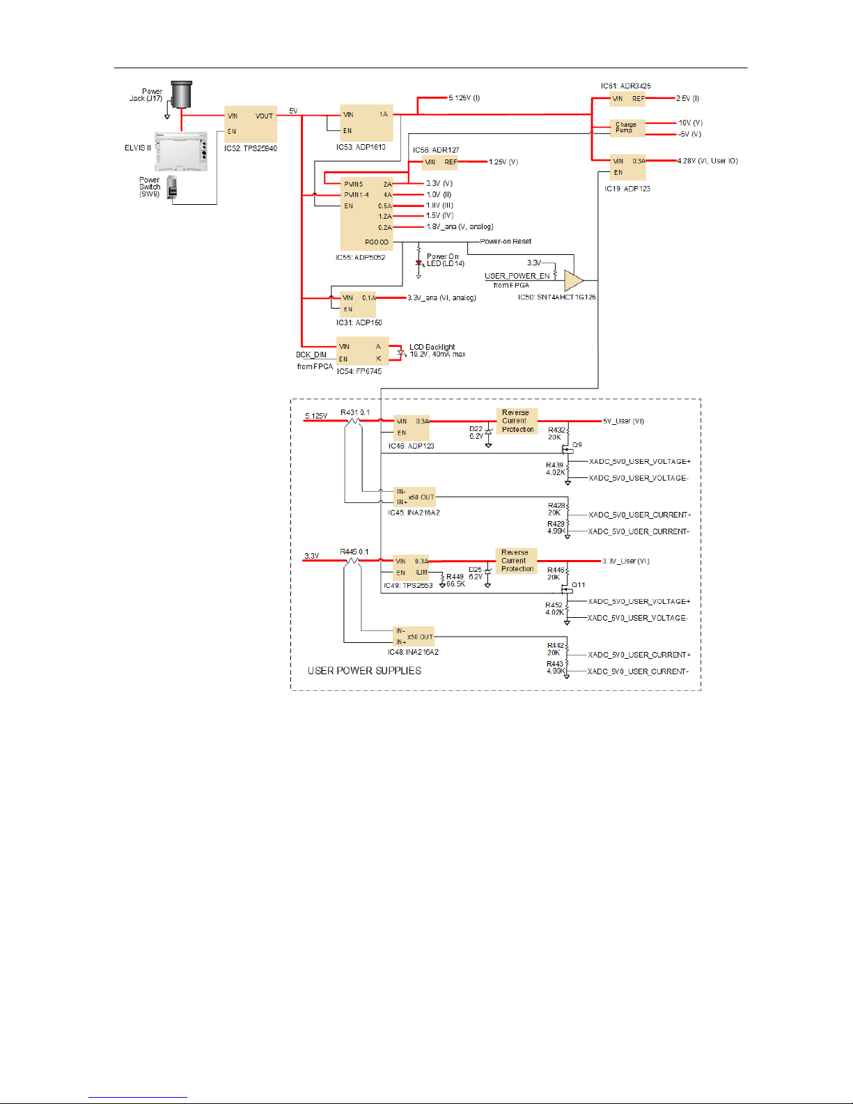
Figure 3. Power Circuit Overview
Voltage regulator circuits from Analog Devices create the required 3.3 V, 1.8 V, 1.5 V, and 1.0 V
supplies from the main power input. Table 1 provides additional information (typical currents
depend strongly on FPGA configuration and the values provided are typical of medium
size/speed designs).
NI Digital System Development Board User Manual | © National Instruments | 7
Page 8
Table 1. DSDB Power Supplies
Supply Circuits Device
Current
(max/typical)
5.125 V User Voltage, Analog Reference,
Buffers for User IO
3.3 V FPGA I/O, USB ports, Clocks,
Ethernet, SD slot, Flash, HDMI, User
IC53:
ADP1613
IC55#1:
ADP5052
Voltage, LCD, touch panel, OLED
1.0 V FPGA, Ethernet Core IC55#2:
ADP5052
1.8 V FPGA Auxiliary, Ethernet I/O, USB
OTG
IC55#3:
ADP5052
1.5 V DDR3 IC55#4:
ADP5052
1.8 V XADC Analog IC26#5:
ADP5052
3.3 V Audio Analog IC6:
ADP150
10 V Analog Output Stage D28, C351,
C349
1 A/0.02 to 0.5 A
2.5 A/0.1 A to
2A
4 A/0.2 A to 4 A
1.2 A/0.1 A to
0.5 A
1.2 A/0.1 A to
1.2 A
200 mA/20 mA
150 mA/50 mA
15 mA/2 mA
-5 V Analog Output Stage D29, C355,
C356
1.25 V XADC Precision Reference IC27:
ADR127
2.5 V Reference for DAC and ADC IC61:
ADR3425
19.2 V LCD Backlight IC54:
FP6745
4.28 V Digital User IO Buffers IC19:
ADP123
5V User Voltage IC46:
ADP123
User Voltage IC49:
TPS2553
15 mA/2 mA
5mA/50A
10 mA/50 A
40 mA/0 to
40 mA
0.3 A/2 mA
0.3 A/0 to 0.3 A
0.3 A/0 to 0.3 A
8 | ni.com | NI Digital System Development Board User Manual
Page 9

The supply rails are daisy-chained to follow the Xilinx-recommended start-up sequence.
Flicking the power switch (SW9) will enable the 5.125 V (IC53) rail, which enables the 1 V
digital supply rail, which in turn enables the supply rails 1.8 V, 3.3 V, and 1.5 V. The 1.25 V
reference, 1.8 V analog supply and 10V, -5V charge pumps ramp together with the 3.3 V rail.
Once all the channels of the ADP5052 (IC55) supply reach regulation, the PGOOD signal will
assert, enabling the 3.3 V audio supply, lighting up the power LED (LD14), enabling user
supplies (IC46, IC49) and power supply for user IO buffers (IC19) and de-asserting the
Power-On Reset signal (PS_POR_B) of the Zynq.
Each power supply uses a soft-start ramp of 1-10ms to limit in-rush current. There is an
additional delay of at least 130ms after the power rails reach regulation and before the Power-On
Reset signal de-assert to allow for the PS_CLK (IC22) to stabilize.
Input Power Monitoring
The DSDB includes a TPS25940i power monitoring switch placed on the 5 V input power rail.
This circuit provides input over and under voltage protection, fast response short-circuit
protection, and slew rate controlled startup to limit inrush current. In case the input supply
voltage is outside the operating range of 4.6 V to 5.5 V, or if the current consumption exceeds
4.4 A, the TPS25940 will turn off the board power.
User Power Supplies
The DSDB provides two user power supplies, 5 V and 3.3 V. The 5 V user supply is available
at the MXP connector, while the 3.3 V is accessible at the PMODs (JA, JB, JC), MXP connector
(J4) and in the digital breadboard (BB3). Each of these two power supplies are able to source up
to 0.3 A and provide the following protection features:
• Short-circuit protection
• 0.3 A current limitation
• Reverse current protection
• Zener protection from accidental shorts to a higher voltage
• Protection from accidental shorts to a reverse polarity voltage
Both of these user supplies turn on automatically after the 5.125 V and FPGA supplies (3.3 V,
1 V, 1.8 V, 1.5 V) are in regulation and the PGOOD signal is asserted. As soon as the PGOOD
signal is deactivated, these user supplies turn off. Alternatively, the user has the ability to disable
these outputs from the FPGA by driving the USER_POWER_EN signal low.
Besides disabling user supplies the USER_POWER_EN signal will also deactivate, the 4.28 V
voltage, which is powering the buffers on the digital IOs that go to PMODs (JA, JB, JC), MXP
(J4) and digital breadboard. This way, the communication between FPGA and the above
mentioned expansion connectors is interrupted.
NI Digital System Development Board User Manual | © National Instruments | 9
Page 10
User Power Supplies Monitoring
The users have the ability to monitor the power of the two user supplies (3.3 V and 5 V) using
the dual channel analog-to-digital converter inside the Zynq (XADC). Both current and voltage
information from the two user supplies are routed to auxiliary analog inputs to the XADC as
differential pairs.
Table 2. Analog Input Pinout
Signal XADC port FPGA pin
XADC_5V0_USER_CURRENT+ AD5P E21
XADC_5V0_USER_CURRENT- AD5N D21
XADC_5V0_USER_VOLTAGE+ AD4P D20
XADC_5V0_USER_VOLTAGE- AD4N C20
XADC_3V3_USER_CURRENT+ AD6P G19
XADC_3V3_USER_CURRENT- AD6N F19
XADC_3V3_USER_VOLTAGE+ AD14P E19
XADC_3V3_USER_VOLTAGE- AD14N E20
The XADC core within the Zynq is a dual channel 12-bit analog-to-digital converter capable of
operating at 1 MSPS. Either channel can be driven by any of the auxiliary analog input pairs.
The XADC core is controlled and accessed from the PL via the Dynamic Reconfiguration Port
(DRP). The DRP also provides access to voltage monitors that are present on each of the FPGA’s
power rails, and a temperature sensor that is internal to the FPGA. For more information on using
the XADC core, refer to the Xilinx document 7 Series FPGAs and Zynq-7000 All Programmable
SoC XADC Dual 12-Bit 1 MSPS Analog-to-Digital Converter. It is also possible to access the
XADC core directly using the PS via the PS-XADC interface. This interface is described in full
in chapter 30 of the Zynq Technical Reference Manual.
The 3.3 V/5 V user voltages are sensed directly at the output through a 1/6 voltage divider. Note
that in case the user power supplies are disabled, the measurement signals
XADC_3V3_USER_VOLTAGE+/-, XADC_5V0_USER_VOLTAGE+/- are disconnected and
the XADC will read 0.The equation below shows how to compute voltage from the XADC
number:
10 | ni.com | NI Digital System Development Board User Manual
Page 11

The current information is collected across 0.1 sense resistors (R431, R445) placed in front of
the circuits that generate the user voltages (IC46, IC49). Since both of these circuits are linear
devices, the input current matches the current on the output. The voltage across the sense resistor
is fed into a current sense amplifier with a gain of 50, INA216A2, and divided by 5 before it is
connected to the XADC inputs. The equation below shows how to compute current from the
XADC number:
Zynq AP SoC Architecture
The Zynq AP SoC is divided into two distinct subsystems: The Processing System (PS), and the
Programmable Logic (PL). Figure 4 shows an overview of the Zynq AP SoC architecture, with
the PS colored light green and the PL in yellow. Note that the PCIe Gen2 controller and
Multi-gigabit transceivers are not available on the device found on this board.
NI Digital System Development Board User Manual | © National Instruments | 11
Page 12
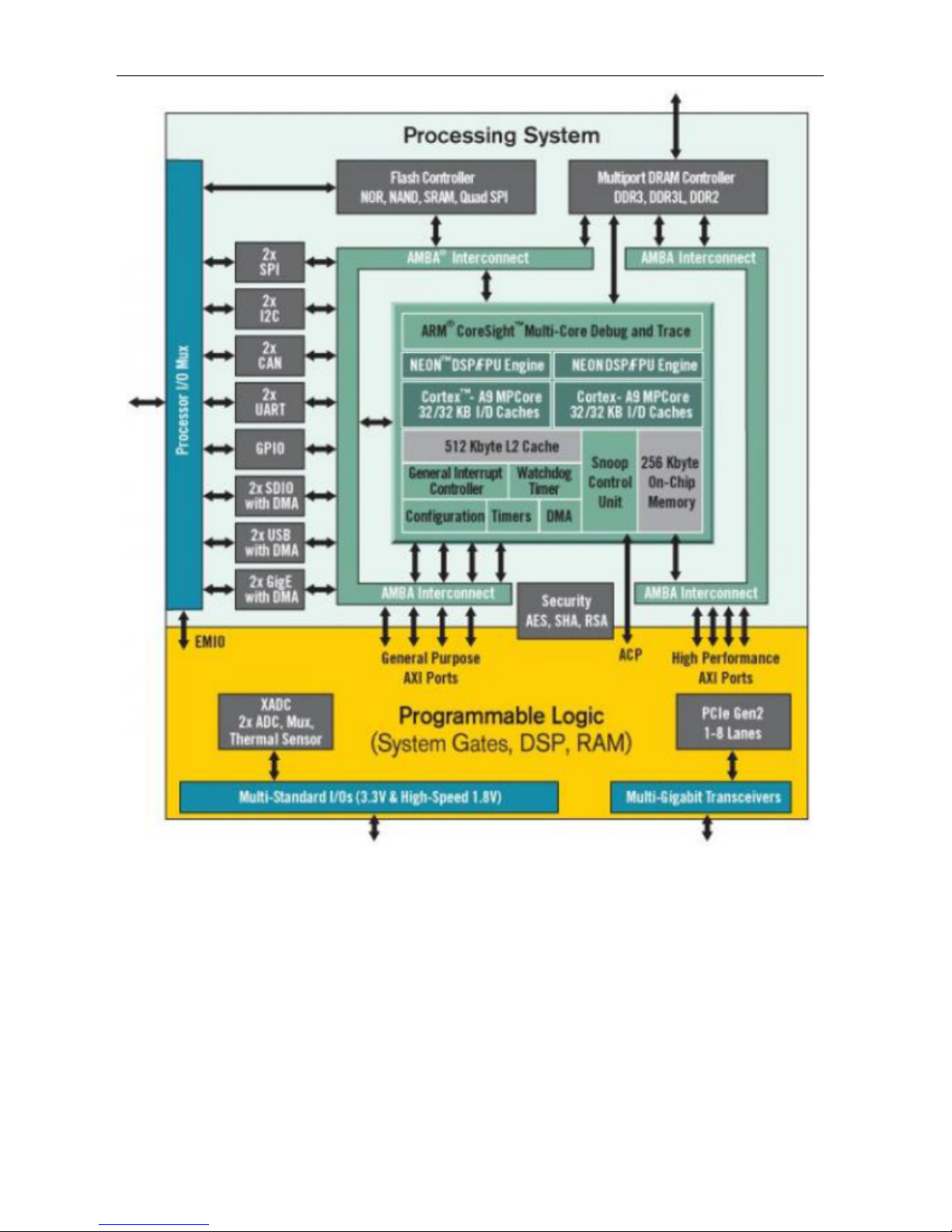
Figure 4. Zynq AP SoC Architecture
The PL is nearly identical to a Xilinx 7-series Artix FPGA, except that it contains several
dedicated ports and buses that tightly couple it to the PS. The PL also does not contain the same
configuration hardware as a typical 7-series FPGA, and it must be configured either directly by
the processor or via the JTAG port.
The PS consists of many components, including the Application Processing Unit (APU, which
includes 2 Cortex-A9 processors), Advanced Microcontroller Bus Architecture (AMBA)
Interconnect, DDR3 Memory controller, and various peripheral controllers with their inputs and
outputs multiplexed to 54 dedicated pins (called Multiplexed I/O, or MIO pins). Peripheral
controllers that do not have their inputs and outputs connected to MIO pins can instead route
their I/O through the PL, via the Extended-MIO (EMIO) interface. The peripheral controllers are
12 | ni.com | NI Digital System Development Board User Manual
Page 13

connected to the processors as slaves via the AMBA interconnect, and contain readable/writable
control registers that are addressable in the processors’ memory space. The programmable logic
is also connected to the interconnect as a slave, and designs can implement multiple cores in the
FPGA fabric that each also contain addressable control registers. Furthermore, cores
implemented in the PL can trigger interrupts to the processors (connections not shown in
Figure 4) and perform DMA accesses to DDR3 memory.
There are many aspects of the Zynq AP SoC architecture that are beyond the scope of this
document. For a complete and thorough description, refer to the Zynq Technical Reference
Manual, available at www.xilinx.com. Table 3 depicts the external components connected to the
MIO pins of the DSDB.
Table 3. MIO Pinout
MIO 500 3.3 V Peripherals Peripherals Peripherals
Pin Pmod SPI Flash GPIO
0 JC9
1 CS
2 DQ0
3 DQ1
4 DQ2
5 DQ3
6 SCLK
7 LED15
8 SLCK FB
9 JC8
10 JC4
11 JC2
12 JC3
13 JC1
14 JC7
15 JF10
NI Digital System Development Board User Manual | © National Instruments | 13
Page 14
MIO 501 1.8 V Peripherals
Pin ENET 0 SDIO 0
16 TXCK
17 TXD0
18 TXD1
19 TXD2
20 TXD3
21 TXCTL
22 RXCK
23 RXD0
24 RXD1
25 RXD2
26 RXD3
27 RXCTL
28-39 Unconnected
40 CCLK
41 CMD
42 D0
43 D1
44 D2
45 D3
46 Unconnected
47 CD
48-51 Unconnected
52 MDC
53 MDIO
14 | ni.com | NI Digital System Development Board User Manual
Page 15

Zynq Configuration
Unlike Xilinx FPGA devices, AP SoC devices such as the Zynq-7020 are designed around the
processor, which acts as a master to the programmable logic fabric and all other on-chip
peripherals in the processing system. This causes the Zynq boot process to be more similar to
that of a microcontroller than an FPGA. This process involves the processor loading and
executing a Zynq Boot Image, which includes a First Stage Bootloader (FSBL), a bitstream for
configuring the programmable logic (optional), and a user application. The boot process is
broken into three stages:
Stage 0
After the DSDB is powered on or the Zynq is reset (in software or by pressing either the red
button labeled PS-SRSTB or PS-PORB), one of the processors (CPU0) begins executing an
internal piece of read-only code called the BootROM. If and only if the Zynq was just powered
on or the reset was triggered with the PS-PORB button, the BootROM will first latch the state
of the mode pins into the mode register (the mode pins are attached to SW8 on the DSDB). If
the BootROM is being executed due to a software or PS-SRSTB triggered reset event, then the
mode pins are not latched and the previous state of the mode register is used. This means that
the DSDB needs a power cycle to register any change in the programming mode switch (SW8).
Next, the BootROM copies an FSBL from the form of non-volatile memory specified by the
mode register to the 256 KB of internal RAM within the APU (called On-Chip Memory, or
OCM). The FSBL must be wrapped up in a Zynq Boot Image in order for the BootROM to
properly copy it. The last thing the BootROM does is hand off execution to the FSBL in OCM.
Stage 1
During this stage, the FSBL first finishes configuring the PS components, such as the DDR
memory controller. Then, if a bitstream is present in the Zynq Boot Image, it is read and used to
configure the PL. Finally, the user application is loaded into memory from the Zynq Boot Image,
and execution is handed off to it.
Stage 2
The last stage is the execution of the user application that was loaded by the FSBL. This can be
any sort of program, from a simple “Hello World” design, to a Second Stage Boot loader used
to boot an operating system like Linux. For a more thorough explanation of the boot process,
refer to Chapter 6 of the Zynq Technical Reference Manual.
The DSDB supports three different boot modes: microSD, Quad-SPI Flash, and JTAG. The boot
mode is selected using the Mode switch (SW8), which affects the state of the Zynq configuration
pins after power-on.
The three boot modes are described in the following sections.
NI Digital System Development Board User Manual | © National Instruments | 15
Page 16

microSD Boot Mode
The DSDB supports booting from a microSD card inserted into connector J15. The following
procedure will allow you to boot the Zynq from microSD:
1. Format the microSD card with a FAT32 file system.
2. Copy the Zynq Boot Image created with Xilinx SDK to the microSD card.
3. Rename the Zynq Boot Image on the microSD card to BOOT.bin.
4. Eject the microSD card from your computer and insert it into connector J15 on the DSDB.
5. Set SW8 to
6. Turn the board on. The board will now boot the image on the microSD card.
SD.
Quad-SPI Boot Mode
The DSDB has an onboard 128-Mbit Quad-SPI serial Flash that the Zynq can boot from. Vivado
and Xilinx SDK can be used to generate a Zynq boot image and program it into the Quad-SPI
flash using the USB-JTAG port. Once a boot image has been programmed into the Quad-SPI
flash, do the following to boot the DSDB:
1. Set SW8 to QSPI.
2. Turn the board on. The board will now boot the image stored in the Quad-SPI flash.
JTAG Boot Mode
When placed in JTAG boot mode, the processor will wait until software is loaded by a host
computer using the Xilinx tools. After software has been loaded, it is possible to either let the
software begin executing, or step through it line by line using Xilinx SDK.
It is also possible to directly configure the PL over JTAG, independent of the processor. This can
be done using iMPACT or the Vivado Hardware Server.
The DSDB is configured to boot in Cascaded JTAG mode, which allows the PS to be accessed
via the same JTAG port as the PL. It is also possible to boot the DSDB in Independent JTAG
mode by loading a jumper in JP1 and shorting it. This will cause the PS to not be accessible from
the onboard JTAG circuitry, and only the PL will be visible in the scan chain. To access the PS
over JTAG while in independent JTAG mode, users will have to route the signals for the PJTAG
peripheral over EMIO, and use an external device to communicate with it.
Connecting to NI ELVIS
The DSDB is fully integrated with the NI ELVIS platform, which features 12 of the most
commonly used instruments in the laboratory including an oscilloscope, digital multimeter,
function generator, variable power supplies, digital reader/writer, two- and three-wire
current-voltage analyzers, and a Bode analyzer. Integration with the NI ELVIS platform gives
students the ability to build comprehensive test benches and analog mixed-signal circuits that
can be designed and tested in one platform. The DSDB is also capable of running standalone
when the advanced functionality of the NI ELVIS is not required.
16 | ni.com | NI Digital System Development Board User Manual
Page 17

The signals from the NI ELVIS edge connector are routed to the Power breadboard header, the
NI ELVIS Analog breadboard header, and the programmable logic of the Zynq. The connections
are described in Tables 4 and 5 below. NI ELVIS pins not listed in the tables below are not
connected to any device on the DSDB. Note that +5 V from this connector is also used to power
the entire board. The GND pins of the NI ELVIS connector, the ground plane of the DSDB, and
the pins labeled GND on the breadboard headers are all connected. For further information on
the functionality of the pins on the NI ELVIS connector, please refer to the NI ELVIS
documentation.
Table 4. NI ELVIS breadboard connections
NI ELVIS Pin Zynq Pin
DIO0 Y20
DIO1 AA16
DIO2 Y19
DIO3 AB16
DIO4 AA18
DIO5 AB15
DIO6 Y18
DIO7 AA14
DIO8 T19
DIO9 AA19
DIO10 U20
DIO11 AB19
DIO12 U10
DIO13 AA17
DIO14 W20
DIO15 AB17
PFI8 N19
PFI9 AB20
PFI12 R21
NI Digital System Development Board User Manual | © National Instruments | 17
Page 18

Table 5. NI ELVIS Zynq Connections
NI ELVIS Pin Breadboard Header Breadboard Pin
+15V Power +15V
-15V Power -15V
+5V Power +5V
VPS+ Power VPS+
VPS- Power VPS-
AIGND Analog AIGND
AISENSE Analog AISNS
AO0 Analog AO0
AO1 Analog AO1
AI0+ Analog AI0+
AI0- Analog AI0-
AI1+ Analog AI1+
AI1- Analog AI1-
AI2+ Analog AI2+
AI2- Analog AI2-
SPI Flash
The DSDB features a Quad-SPI serial flash device, the Spansion S25FL128S. The Multi-I/O SPI
Flash memory is used to provide non-volatile code and data storage. It can be used to initialize
the PS subsystem as well as configure the PL subsystem (bitstream).
The relevant device attributes are:
• 128 Mbit
• x1, x2, and x4 support
• Speeds up to 94 MHz. In Quad-SPI mode, this translates to 376 Mbps
• Powered from 3.3 V
The SPI Flash connects to the Zynq-7000 AP SoC supporting up to Quad-I/O SPI interface. This
requires connection to specific pins in MIO Bank 0/500, specifically MIO[1:6,8] as outlined in
the Zynq datasheet. Quad-SPI feedback mode is used, thus qspi_sclk_fb_out/MIO[8] is left to
freely toggle and is connected only to a 20K pull-up resistor to 3.3 V. This allows a QSPI clock
frequency greater than FQSPICLK2.
18 | ni.com | NI Digital System Development Board User Manual
Page 19

DDR3 Memory
The DSDB includes two Micron MT41J128M16JT-125 or MT41K128M16JT-125 DDR3
memory components creating a single rank, 32-bit wide interface and a total of 512MiB of
capacity. The DDR3 is connected to the hard memory controller in the Processor Subsystem
(PS), as outlined in the Xilinx Zynq TRM (ug585).
The PS incorporates an AXI memory port interface, a DDR3 controller, the associated PHY, and
a dedicated I/O bank. Interface speeds of up to 525MHz/1050 Mbps are supported.
DDR3 uses 1.5 V SSTL15 single-ended and DIFF_SSTL15 differential signaling. Address and
control signals are routed in a tree topology with minimal stubs and series termination scheme.
Data signals follow a point-to-point scheme and benefit from on-die termination (ODT) on both
ends.
The target trace impedance is 40 (±10%) for single-ended signals, and 80 (±10%) for
differential. A feature called DCI (Digitally Controlled Impedance) is used to match the drive
strength and termination impedance of the PS pins to the trace impedance. On the memory side,
each chip calibrates its on-die termination and drive strength using a 240 resistor on the ZQ
pin.
Due to layout reasons, the two lower data byte groups (DQ[0-7], DQ[8-15]) were swapped. To
the same effect, the data bits inside byte groups were swapped as well. These changes are
transparent to the user. Appropriate Xilinx PCB guidelines were followed during design.
Both the memory chips and the PS DDR bank are powered from the 1.5 V supply. The mid-point
reference of 0.75 V is created with a simple resistor divider and is available to the Zynq as
external reference.
For proper operation it is essential that the PS memory controller is configured properly. Settings
range from memory timings to the board trace delays. For your convenience, the Zynq preset file
for the DSDB is provided on the Digilent DSDB Resource Center and can be used to
automatically configure the correct parameters.
For best DDR3 performance, DRAM training is enabled for write leveling, read gate, and read
data eye options in the PS Configuration Tool in Xilinx tools. Training is done dynamically by
the controller to account for board delays, process variations, and thermal drift. Optimum
starting values for the training process are the board delays (propagation delays) for certain
memory signals. process variations, and thermal drift. Optimum starting values for the training
process are the board delays (propagation delays) for certain memory signals.
Board delays are specified for each of the data byte groups in absolute terms and then relative to
CLK. These parameters are board-specific and were calculated from the PCB trace length
reports.
For more details on memory controller operation, refer to the Xilinx Zynq TRM (ug585).
NI Digital System Development Board User Manual | © National Instruments | 19
Page 20

USB UART Bridge (Serial Port)
The DSDB includes an FTDI FT2232HQ USB-UART bridge (attached to connector J13) that
lets you use PC applications to communicate with the board using standard Windows COM port
commands. Free USB-COM port drivers, available from www.ftdichip.com www.ftdichip.com
under the Virtual Com Port or VCP heading, convert USB packets to UART/serial port data.
Serial port data is exchanged with the Zynq using a two-wire serial port (TXD/RXD). After the
drivers are installed, I/O commands can be used from the PC directed to the COM port to
produce serial data traffic on the Zynq pins. The port is tied to FPGA pins and can be used in
combination with the UART 1 or UART 0 controllers via EMIO.
Two on-board status LEDs provide visual feedback on traffic flowing through the port: the
transmit LED (LD10) and the receive LED (LD9). Signal names that imply direction are from
the point-of-view of the DTE (Data Terminal Equipment), in this case the PC.
The FT2232HQ is also used as the controller for the Digilent USB-JTAG circuitry, but the
USB-UART and USB-JTAG functions behave entirely independent of one another.
Programmers interested in using the UART functionality of the FT2232 within their design do
not need to worry about the JTAG circuitry interfering with the UART data transfers, and
vice-versa. The combination of these two features into a single device allows the DSDB to be
programmed and communicated with via UART from a computer attached with a single Micro
USB cable.
microSD Slot
The DSDB provides a microSD slot (J15) for non-volatile external memory storage as well as
booting the Zynq. The slot is wired to Bank 1/501 MIO[40-47], including Card Detect. On the
PS side peripheral SDIO 0 is mapped out to these pins and controls communication with the SD
card. The pinout can be seen in Table 6. The peripheral controller supports 1-bit and 4-bit SD
transfer modes, but does not support SPI mode. Based on the Zynq TRM, SDIO host mode is the
only mode supported.
Table 6. microSD Pinout
Signal Name Description Zynq Pin SD Slot Pin
SD_D0 Data[0] MIO42 7
SD_D1 Data[1] MIO43 8
SD_D2 Data[2] MIO44 1
SD_D3 Data[3] MIO45 2
SD_CCLK Clock MIO40 5
SD_CMD Command MIO41 3
SD_CD Card Detect MIO47 9
20 | ni.com | NI Digital System Development Board User Manual
Page 21

The SD slot is powered from 3.3 V, but is connected through MIO Bank 1/501 (1.8 V).
Therefore, a TI TXS02612 level shifter performs this translation. The TXS02612 is actually
2-port SDIO port expander, but only its level shifter function is used. Mapping out the correct
pins and configuring the interface is handled by the DSDB board definition file.
Both low speed and high speed cards are supported, the maximum clock frequency being
50 MHz. A Class 4 card or better is recommended.
Refer to microSD Boot Mode for information on how to boot from an SD card. For more
information, consult the Xilinx Zynq TRM (ug585).
USB HID Host
The Auxiliary Function microcontroller (Microchip® PIC24FJ128) provides USB HID host
capability. Firmware in the microcontroller can drive a mouse or a keyboard attached to the type
A USB connector at J9 labeled “USB HID”. The PIC24 then emulates a PS/2 device towards the
FPGA over two PS/2 ports. Port 0 is always keyboard, while port 1 is always mouse. Hub
support is not currently available, so only a single mouse or keyboard can be used at any time.
Table 7. USB HID Pinout
Function Schematic Net FPGA Pin
PS/2 Keyboard Data PS2_DATA0 R7
Clock PS2_CLK0 Y11
PS/2 Mouse Data PS2_DATA1 Y21
Clock PS2_CLK1 U11
HID Controller
The Auxiliary Function microcontroller hides the USB HID protocol from the FPGA and
emulates an old-style PS/2 bus. The microcontroller behaves just like a PS/2 keyboard or mouse
would. This means new designs can re-use existing PS/2 IP cores. Mice and keyboards that use
the PS/2 protocol use a two-wire serial bus (clock and data) to communicate with a host. On the
DSDB, the microcontroller emulates a PS/2 device, while the FPGA plays the role of the host.
Both the mouse and the keyboard use 11-bit words that include a start bit, data byte (LSB first),
odd parity, and stop bit, but the data packets are organized differently, and the keyboard interface
allows bidirectional data transfers (so the host device can illuminate state LEDs on the
keyboard). Bus timings are shown in Figure 5.
NI Digital System Development Board User Manual | © National Instruments | 21
Page 22

Figure 5. PS/2 Device-to-host Timing Diagram
The clock and data signals are only driven when data transfers occur; otherwise, they are held in
the idle state at logic '1'. This requires that when the PS/2 signals are used in a design, internal
pull-ups must be enabled in the FPGA on the data and clock pins. The clock signal is normally
driven by the device, but may be held low by the host in special cases. The timings define signal
requirements for mouse-to-host communications and bidirectional keyboard communications. A
PS/2 interface circuit can be implemented in the FPGA to create a keyboard or mouse interface.
When a keyboard or mouse is connected to the board, a self-test passed command (0xAA) is sent
to the host. After this, commands may be issued to the device. Since both the keyboard and the
mouse use the same PS/2 port, one can tell the type of device connected using the device ID.
This ID can be read by issuing a Read ID command (0xF2). Also, a mouse sends its ID (0x00)
right after the self-test passed command, which distinguishes it from a keyboard.
Keyboard
PS/2 uses open-collector drivers so the keyboard, or an attached host device, can drive the
two-wire bus (if the host device will not send data to the keyboard, then the host can use
input-only ports).
PS/2-style keyboards use scan codes to communicate key press data. Each key is assigned a code
that is sent whenever the key is pressed. If the key is held down, the scan code will be sent
repeatedly about once every 100ms. When a key is released, an F0 key-up code is sent, followed
by the scan code of the released key. If a key can be shifted to produce a new character (like a
capital letter), then a shift character is sent in addition to the scan code, and the host must
determine which ASCII character to use. Some keys, called extended keys, send an E0 ahead of
the scan code (and they may send more than one scan code). When an extended key is released,
an E0 F0 key-up code is sent, followed by the scan code. Scan codes for most keys are shown in
Figure 6.
22 | ni.com | NI Digital System Development Board User Manual
Page 23

Figure 6. Keyboard Scan Codes
A host device can also send data to the keyboard. Table 8 shows a list of some common
commands a host might send.
Table 8. Keyboard Commands
Command Action
ED Set Num Lock, Caps Lock, and Scroll Lock LEDs. Keyboard
returns FA after receiving ED, then host sends a byte to set
LED status: bit 0 sets Scroll Lock, bit 1 sets Num Lock, and bit
2 sets Caps lock. Bits 3 to 7 are ignored.
EE Echo (test). Keyboard returns EE after receiving EE.
F3 Set scan code repeat rate. Keyboard returns F3 on receiving
FA, then host sends second byte to set the repeat rate.
FE Resend. FE directs keyboard to re-send most recent scan code.
FF Reset. Resets the keyboard.
The keyboard can send data to the host only when both the data and clock lines are high (or idle).
Because the host is the bus master, the keyboard must check to see whether the host is sending
data before driving the bus. To facilitate this, the clock line is used as a clear to send” signal. If
the host drives the clock line low, the keyboard must not send any data until the clock is released.
The keyboard sends data to the host in 11-bit words that contain a '0' start bit, followed by 8-bits
of scan code (LSB first), followed by an odd parity bit, and terminated with a '1' stop bit. The
keyboard generates 11 clock transitions (at 20 to 30 kHz) when the data is sent, and data is valid
on the falling edge of the clock.
NI Digital System Development Board User Manual | © National Instruments | 23
Page 24

Mouse
Once entered in stream mode and data reporting enabled, the mouse outputs a clock and data
signal when it is moved; otherwise, these signals idle in logic '1.' Each time the mouse is moved,
three 11-bit words are sent from the mouse to the host device, as shown in Figure 11. Each of
the 11-bit words contains a '0' start bit, followed by 8 bits of data (LSB first), followed by an odd
parity bit, and terminated with a '1' stop bit. Thus, each data transmission contains 33 bits, where
bits 0, 11, and 22 are '0' start bits, and bits 11, 21, and 33 are '1' stop bits. The three 8-bit data
fields contain movement data as shown in the figure above. Data is valid at the falling edge of
the clock, and the clock period is 20 to 30 kHz.
The mouse assumes a relative coordinate system wherein moving the mouse to the right
generates a positive number in the X field, and moving to the left generates a negative number.
Likewise, moving the mouse up generates a positive number in the Y field, and moving down
represents a negative number (the XS and YS bits in the status byte are the sign bits – a '1'
indicates a negative number). The magnitude of the X and Y numbers represent the rate of mouse
movement: the larger the number, the faster the mouse is moving (the XV and YV bits in the
status byte are movement overflow indicators – a '1' means overflow has occurred). If the mouse
moves continuously, the 33-bit transmissions are repeated every 50ms or so. The L and R fields
in the status byte indicate Left and Right button presses (a '1' indicates the button is being
pressed).
Figure 7. Mouse Data Format
The microcontroller also supports Microsoft® IntelliMouse®-type extensions for reporting back
a third axis representing the mouse wheel, as shown in Table 9.
Table 9. Microsoft Intellimouse Type Extensions, Commands, and Actions
Command Action
EA Set stream mode. The mouse responds with “acknowledge”
(0xFA) then resets its movement counters and enters stream
mode.
F4 Enable data reporting. The mouse responds with
“acknowledge” (0xFA) then enables data reporting and resets
its movement counters. This command only affects behavior in
stream mode. Once issued, mouse movement will
automatically generate a data packet.
F5 Disable data reporting. The mouse responds with
24 | ni.com | NI Digital System Development Board User Manual
“acknowledge” (0xFA) then disables data reporting and resets
its movement counters.
Page 25

Table 9. Microsoft Intellimouse Type Extensions, Commands, and Actions (Continued)
Command Action
F3 Set mouse sample rate. The mouse responds with
“acknowledge” (0xFA) then reads one more byte from the
host. This byte is then saved as the new sample rate, and a new
“acknowledge” packet is issued.
FE Resend. FE directs mouse to re-send last packet.
FF Reset. The mouse responds with “acknowledge” (0xFA) then
enters reset mode.
Ethernet
The DSDB uses a Realtek RTL8211E-VL PHY to implement a 10/100/1000 Ethernet port for
network connection. The PHY connects to MIO Bank 501 (1.8 V) and interfaces to the
Zynq-7000 AP SoC via reduced gigabit media-independent interface (RGMII) for data and
MDIO for management. The auxiliary interrupt (ETH_INT_B) and reset (ETH_RST_B) signals
connect to PL pins to be accessed via EMIO.
After power-up, the PHY starts with Auto Negotiation enabled, advertising 10/100/1000 link
speeds and full duplex. If there is an Ethernet-capable partner connected, the PHY automatically
establishes a link with it even with the Zynq not configured.
Two status indicator LEDs are on-board near the RJ-45 connector that indicate traffic (LD12)
and valid link state (LD11). Table 10 shows the default behavior.
Table 10. Ethernet Status LEDs
Function Designator State Description
LINK LD11 Steady Link 10/100/1000
Blinking 0.4s ON, 2s OFF Link, Energy Efficient
Ethernet (EEE) mode
ACT LD12 Blinking Transmitting or Receiving
The Zynq incorporates two independent Gigabit Ethernet Controllers. They implement a
10/100/1000 half/full duplex Ethernet MAC. Of these two, GEM 0 can be mapped to the MIO
pins where the PHY interfaces. Since the MIO bank is powered from 1.8 V, the RGMII interface
uses 1.8 V HSTL Class 1 drivers. For this I/O standard an external reference of 0.9 V is provided
in bank 501 (PS_MIO_VREF). Mapping out the correct pins and configuring the interface is
handled by the PS preset, part of the board definition files.
The MDIO bus is available for management. The RTL8211E-VL is assigned the 5-bit address
00001 on the MDIO bus. With simple register read and write commands, status information can
NI Digital System Development Board User Manual | © National Instruments | 25
Page 26

be read out or configuration changed. The Realtek PHY follows industry-standard register map
for basic configuration.
The RGMII specification calls for the receive (RXC) and transmit clock (TXC) to be delayed
relative to the data signals (RXD[0:3], RXCTL and TXD[0:3], TXCTL). Xilinx PCB guidelines
also require this delay to be added. The RTL8211E-VL is capable of inserting a 2ns delay on
both the TXC and RXC so that board traces do not need to be made longer. RTL8211E-VL is
capable of inserting a 2 ns delay on both the TXC and RXC so that board traces do not need to
be made longer.
The PHY is clocked from the same 50 MHz oscillator (IC41) that clocks the PS too. The
parasitic capacitance of the two loads is low enough to be driven from a single source.
For more information on using the Gigabit Ethernet MAC, refer to the Xilinx Zynq TRM
(ug585).
The sticker with the Ethernet MAC address is affixed to the bottom of the board. It can also be
read out programmatically from a special read-only section of the on-board quad SPI Flash. This
one-time programmable (OTP) section is factory written and is separate from the regular Flash
memory space. It can be read out with the special OTP Read (0x4B) command. The MAC is
located in the six bytes starting at address 0x20. The byte order is big-endian, so the most
significant byte starts at the lower address. The three most significant bytes correspond to the
Digilent Organizationally Unique Identifier (OUI) which is 00-18-3E.
The MAC is located in the first non-reserved OTP region of the flash. It is programmed and the
whole region locked during manufacturing, so it is shipped read-only. The rest of the OTP
regions are available for user programming.
See the Spansion Flash datasheet for more information.
OLED
A Univision Technology Inc. UG-2832HSWEG04 is loaded on the DSDB. It is a white
monochrome, 128 × 32, 0.910-in. organic LED display matrix bundled with a Solomon Systech
SSD1306 display controller. The display data interface towards the Zynq programmable logic is
a 4-wire serial peripheral interface (SPI). The 4 wires in controller-terminology are CS#, D/C#,
SDIN, and SCLK, but CS# is hard-wired to ground. This adds to the reset and two power control
signals for proper start-up sequencing. The signals are summarized in Table 11.
26 | ni.com | NI Digital System Development Board User Manual
Page 27

Table 11. OLED Signal Description
Signal Description Polarity FPGA Pin
RES# Reset Active-low E16
CS# Chip select (always active) Active-low N/A
D/C# Data (high)/Command (low) Both H15
SCLK Serial Clock Active-hig
J15
h
SDIN Serial Data Active-hig
J17
h
VBAT# Power enable for internal power supply Active-low L17
VDD# Power enable for digital power Active-low J16
The serial interface is synchronous to SCLK and must conform to the timing specifications
below. In most cases, a 10 MHz SCLK and data sent on the falling edge should work.
Figure 8. Serial Interface Timing Diagram
Figure 9. OLED Serial Interface Bit Ordering
NI Digital System Development Board User Manual | © National Instruments | 27
Page 28

Table 12. Timing Diagram Symbols and Parameters
Symbol Parameter Min Typ Max Unit
tcycle Clock Cycle Time 100 - - ns
tAS Address Setup Time 15 - - ns
tAH Address Hold Time 15 - - ns
tCSS Chip Select Setup Time 20 - - ns
tCSH Chip Select Hold Time 10 - - ns
tDSW Write Data Setup Time 15 - - ns
tDHW Write Data Hold Time 15 - - ns
tCLKL Clock Low Time 20 - - ns
tCLKH Clock High Time 20 - - ns
tR Rise Time - - 40 ns
tF Fall Time - - 40 ns
Start‐upsequence:
1. Power up VDD by pulling OLED_VDD low. Wait 1 ms.
2. Pulse RES# low for at least 3 s.
3. Send initialization/configuration commands (see Table 13).
4. Power up VBAT by pulling OLED_VBAT low. Wait 100 ms for voltage to stabilize.
5. Power up VBAT by pulling OLED_VBAT low. Wait 100 ms for voltage to stabilize.
6. Clear screen by writing zero to the display buffer.
7. Send Display On command (0xAF).
Table 13. OLED Configuration Commands
Command Function Command Bytes
Charge pump enable 0x8D, 0x14
Set pre-charge period 0xD9, 0xF1
Contrast control 0x81, 0x0F
Column inversion disable 0xA0
Scan direction 0xC0
28 | ni.com | NI Digital System Development Board User Manual
Page 29

Table 13. OLED Configuration Commands (Continued)
Command Function Command Bytes
COM pins configuration 0xDA, 0x00
Addressing mode: horizontal 0x20
After start-up, writing to the display is done by sending data bytes over the serial interface (D/C#
high). Each data bit corresponds to a pixel with the addressing mode, inversion, and scan
direction settings determining exactly which.
VGA Port
The DSDB board uses 18 programmable logic pins to create an analog VGA output port. This
translates to 16-bit color depth and two standard sync signals (HS – Horizontal Sync, and VS –
Vertical Sync). The digital-to-analog conversion is done using a simple R-2R resistor ladder.
The ladder works in conjunction with the 75- termination resistance of the VGA display to
create 32 and 64 analog signal levels; red, blue, and green VGA signals. This circuit, shown in
Figure 9, produces video color signals that proceed in equal increments between 0 V (fully off)
and 0.7 V (fully on). With 5 bits each for red and blue and 6 bits for green, 65,536 (32 × 32 × 64)
different colors can be displayed, one for each unique 16-bit pattern.
A video controller circuit must be created in programmable logic to drive the sync and color
signals with the correct timing in order to produce a working display system.
VGA System Timing
VGA signal timings are specified, published, copyrighted, and sold by the VESA organization.
The following VGA system timing information is provided as an example of how a VGA
monitor might be driven in 640 by 480 mode.
Note For more precise information, or for information on other VGA frequencies,
refer to documentation available at the VESA website.
CRT-based VGA displays use amplitude-modulated moving electron beams (or cathode rays) to
display information on a phosphor-coated screen. LCD displays use an array of switches that can
impose a voltage across a small amount of liquid crystal, thereby changing light permittivity
through the crystal on a pixel-by-pixel basis. Although the following description is limited to
CRT displays, LCD displays have evolved to use the same signal timings as CRT displays (so
the signals discussion below pertains to both CRTs and LCDs). Color CRT displays use three
electron beams (one for red, one for blue, and one for green) to energize the phosphor that coats
the inner side of the display end of a cathode ray tube (see Figure 10).
NI Digital System Development Board User Manual | © National Instruments | 29
Page 30

Figure 10. Color CRT Display
Electron beams emanate from electron guns which are finely-pointed heated cathodes placed in
close proximity to a positively charged annular plate called a grid. The electrostatic force
imposed by the grid pulls rays of energized electrons from the cathodes, and those rays are fed
by the current that flows into the cathodes. These particle rays are initially accelerated towards
the grid, but they soon fall under the influence of the much larger electrostatic force that results
from the entire phosphor-coated display surface of the CRT being charged to 20 kV (or more).
The rays are focused to a fine beam as they pass through the center of the grids, and then they
accelerate to impact on the phosphor-coated display surface. The phosphor surface glows
brightly at the impact point, and it continues to glow for several hundred microseconds after the
beam is removed. The larger the current fed into the cathode, the brighter the phosphor will glow.
Between the grid and the display surface, the beam passes through the neck of the CRT where
two coils of wire produce orthogonal electromagnetic fields. Because cathode rays are composed
of charged particles (electrons), they can be deflected by these magnetic fields. Current
waveforms are passed through the coils to produce magnetic fields that interact with the cathode
rays and cause them to transverse the display surface in a raster pattern, horizontally from left
to right and vertically from top to bottom, as shown in Figure 11. As the cathode ray moves over
the surface of the display, the current sent to the electron guns can be increased or decreased to
change the brightness of the display at the cathode ray impact point.
Information is only displayed when the beam is moving in the forward direction (left to right and
top to bottom), and not during the time the beam is reset back to the left or top edge of the display.
Much of the potential display time is therefore lost in blanking periods when the beam is reset
and stabilized to begin a new horizontal or vertical display pass. The size of the beams, the
frequency at which the beam can be traced across the display, and the frequency at which the
electron beam can be modulated determine the display resolution.
30 | ni.com | NI Digital System Development Board User Manual
Page 31

Modern VGA displays can accommodate different resolutions, and a VGA controller circuit
dictates the resolution by producing timing signals to control the raster patterns. The controller
must produce synchronizing pulses at 3.3 V (or 5 V) to set the frequency at which current flows
through the deflection coils, and it must ensure that video data is applied to the electron guns at
the correct time. Raster video displays define a number of rows that corresponds to the number
of horizontal passes the cathode makes over the display area, and a number of columns that
corresponds to an area on each row that is assigned to one picture element, or pixel. Typical
displays use from 240 to 1200 rows and from 320 to 1600 columns. The overall size of a display
and the number of rows and columns determines the size of each pixel.
Figure 11. VGA Horizontal Synchronization
Video data typically comes from a video refresh memory; with one or more bytes assigned to
each pixel location (the DSDB uses 16 bits per pixel). The controller must index into video
memory as the beams move across the display, and retrieve and apply video data to the display
at precisely the time the electron beam is moving across a given pixel.
A VGA controller circuit must generate the HS and VS timings signals and coordinate the
delivery of video data based on the pixel clock. The pixel clock defines the time available to
display one pixel of information. The VS signal defines the refresh frequency of the display, or
the frequency at which all information on the display is redrawn. The minimum refresh
NI Digital System Development Board User Manual | © National Instruments | 31
Page 32

frequency is a function of the display’s phosphor and electron beam intensity, with practical
refresh frequencies falling in the 50 Hz to 120 Hz range. The number of lines to be displayed at
a given refresh frequency defines the horizontal retrace frequency. For a 640-pixel by 480-row
display using a 25 MHz pixel clock and 60 ±1 Hz refresh, the signal timings shown in Figure 12
can be derived. Timings for sync pulse width and front and back porch intervals (porch intervals
are the pre- and post-sync pulse times during which information cannot be displayed) are based
on observations taken from actual VGA displays.
Figure 12. Signal Timings for a 640-pixel by 480 Row Display Using a 25 MHz Pixel Clock
and 60 Hz Vertical Refresh
A VGA controller circuit, such as the one diagramed in Figure 13, decodes the output of a
horizontal-sync counter driven by the pixel clock to generate HS signal timings. You can use this
counter to locate any pixel location on a given row. Likewise, the output of a vertical-sync
counter that increments with each HS pulse can be used to generate VS signal timings, and you
can use this counter to locate any given row. These two continually running counters can be used
to form an address into video RAM. No time relationship between the onset of the HS pulse and
the onset of the VS pulse is specified, so you can arrange the counters to easily form video RAM
addresses, or to minimize decoding logic for sync pulse generation.
32 | ni.com | NI Digital System Development Board User Manual
Page 33

Figure 13. VGA Display Controller Block Diagram
HDMI Source/Sink Port
An input and output-capable HDMI Port connects to the programmable logic pins. Over this
connector an HDMI or DVI-compatible video stream can be driven in or out of the DSDB.
Encoding or decoding the HDMI/DVI video stream needs to be implemented in logic, as well as
auxiliary functions, like DDC or CEC. Depending on the actual design, it can take the Source
role driving a monitor/TV display, or behave as a Sink accepting a video stream from any
HDMI/DVI Source, like a laptop or smartphone.
On-board auxiliary buffers and electronic switches control the direction of signals that differ
between Source and Sink. These signals are summarized Table 14.
Table 14. HDMI Signal Direction in Source and Sink Roles
Directio
n (Zynq
Signal Role Description
HPD Source Hot-plug detect; signals the
POW)
Input HDMI_OUT_EN = 1
How to Control
presence of a Sink to a
Sink Output HDMI_OUT_EN = 0
Source
5V0 Source Auxiliary power for Sink Output HDMI_OUT_EN = 1
Sink Input HDMI_OUT_EN = 0
The CEC function is bidirectional by definition, so it is treated the same no matter what role the
port takes. If the CEC function is not used, declare it as input and constrain it to the correct PL
pin to leave other devices on the CEC bus unaffected.
When operating as Sink, the DDC function is required to be implemented so that a connected
Source can read out important characteristics of the device. This can be done by emulating an
I2C-capable EEPROM in programmable logic. Likewise, in Source mode DDC can be used to
find out the capabilities of the connected display.
The HDMI/DVI protocol uses TMDS (Transition-minimized differential signaling) as I/O
standard. It is supported on Zynq by the I/O buffers on the programmable logic side. 50
external parallel termination resistors are provided on-board. HDMI specifications only require
terminations on the Sink side, but optional Source-side terminations reduce reflections, resulting
in improved signal quality. Do not connect powered HDMI/DVI devices to an unpowered
NI Digital System Development Board User Manual | © National Instruments | 33
Page 34

DSDB, as it might result in back-powering the board through the termination resistors.
Resolutions up to 720p (1280 × 720) have been tested.
HDMI and DVI are high-speed source-synchronous serial protocols. Implementations on FPGA
are required to use certain built-in primitives to properly synthesize the correct clock frequency,
serialize the transmission, and keep a lock on the signal. The actual implementation of the
HDMI/DVI protocols is outside the scope of this manual. Vivado IP cores are available for free
from www.github/digilent that can be used to handle this. These IP cores convert the high-speed
serial data to an RGB interface that is very similar to the one used to communicate with a VGA
port.
Touchscreen Display
The DSDB has a TFT-LCD with a capacitive touch panel mounted on the LCD. The LCD is a
5” diagonal, 800 x 480 RGB display with a 24-bit color depth. The touch panel size has been
scaled to the LCD so that every point read from the touch panel can be converted to a RGB pixel
on the TFT-LCD. Although the LCD and touch panel come as an assembly, they have
independent controllers and are driven separately.
LCD Display
The LCD has an ILI6122 timing controller mounted on it which interfaces to the TFT display.
The user has access only to certain pins of the controller, specifically those which are used to
send data to the LCD. In order to access the controller pins the LCD uses a strip connector with
the following pin-out.
Table 15. LCD Control Signals
Pin Signal Description
1 BCK_LED_K Back-light LED cathode. Connected to the FP6745
LED driver
2 BCK_LED_A Back-light LED anode. Connected to the FP6745 LED
driver
3 GND Ground
4 VCC 3.3 V
5 - 12 TFT_R0 - TFT_R7 8-bit data bus corresponding to the red signal.
13 - 20 TFT_G0 -
TFT_G7
8-bit data bus corresponding to the green signal.
21 - 28 TFT_B0 - TFT_B7 8-bit data bus corresponding to the blue signal.
29 GND Ground
30 TFT_DCLK Data clock
34 | ni.com | NI Digital System Development Board User Manual
Page 35

Table 15. LCD Control Signals (Continued)
Pin Signal Description
31 TFT_DISP Display enable, active high
32 TFT_HS Horizontal synchronisation pulse
33 TFT_VS Vertical synchronisation pulse
34 TFT_DE Active video signal
35 NC Not connected
36 GND Ground
37 - 40 NC Not connected
In order to facilitate the dimming of the back-light on the LCD, the FP6745 LED driver has been
used. The user has direct access to the enable pin of the LED-driver; by driving this pin with a
PWM signal the user will obtain a variety of back-light intensities dependent on the duty cycle
of the PWM signal. When driving the back-light with PWM, it is highly recommended to choose
a PWM frequency above 20 kHz, because this circuit may interfere with the audio circuit. Before
starting to use the LCD, the DISP pin must be set to logic high. This pin is an enable pin which
allows the user to turn off the display without interrupting the timing and data flow. When
sending data to the display, the following timing specifications must be respected:
Figure 14. Horizontal Timing
Table 16. Horizontal Timing
Horizontal Input Timing
Parameter Symbol Va l u e Unit
Min. Typ. Max.
Active Area thd — 800 — CLKIN
CLKIN frequency fclk — 33.3 50 MHz
Horizontal line period th 862 1056 1200 CLKIN
NI Digital System Development Board User Manual | © National Instruments | 35
Page 36

Table 16. Horizontal Timing (Continued)
Horizontal Input Timing
Horizontal pulse
width
Horizontal back porch thbp 46 46 46 CLKIN
Horizontal front porch thfp 16 210 354 CLKIN
Min. thpw — 1 — CLKIN
Typ. — — — CLKIN
Max. — 40 — CLKIN
Figure 15. Vertical Timing
Table 17. Vertical Timing
Vertical Input Timing
Parameter Symbol Va l u e Unit
Min. Typ. Max.
Vertical display area tvd – 480 – HS
Vertical line period tv 510 525 650 HS
Vertical pulse width tvpw 1 – 20 HS
Vertical back porch tvbp 23 23 23 HS
Vertical front porch tvfp 7 22 147 HS
These timing constraints are similar to the VGA functionality presented in a previous chapter,
but the timing specifications have to be strictly respected in order to ensure the correct
functionality of the device.
Capacitive Touchscreen
The capacitive touch panel uses an FT5x16 series controller, with which the user can
communicate through an I2C protocol. Similar to the LCD the touch connects to the board using
a strip connector with the following pinout:
36 | ni.com | NI Digital System Development Board User Manual
Page 37

Table 18. Touch Panel Pinout
Pin Signal Description
1 VCC 3.3 V
2 TP_SCK I2C clock signal
3 TP_SDA I2C data signal
4 TP_IRQ Interrupt/wake-up signal
5 TP_RES Reset signal, has a pull-up resistor
6 GND Ground
The addressing mode of the I2C is 7 bit, with the slave address being 0111000 in binary and the
maximum frequency at which the controller can operate is 400 KHz. In addition to the I2C bus,
there are two other signals provided by the controller; the RESET and the INT signal. In order
to reset the touch panel controller, the RESET pin has to be driven low for at least 1 ms. The INT
signal is an I/O signal which will go low while the panel is being touched. Also, when the
FT5x16 is in hibernation, the same INT signal must be used in order to wake the controller up.
When using the INT signal in order to wake the controller, the low pulse generate for the
wake-up sequence must be driven low for 0.5 to 1 ms. The reason for this short period is that the
INT port will act as an interrupt output port after the wake-up.
The following registers can be used in order to obtain a minimal functionality of the touch panel:
This is the device mode register, which is configured to determine the current mode of the
chip.(Read/Write)
Table 19. Device Mode Register
Bit
Address
Address
00h 6:4 Device Mode
Register Name Description
000b Normal operating Mode
[2:0]
001b System Information Mode
(Reserved)
100b FACTORY MODE0 (Reserved)
110b FACTORY MODE1 (Reserved)
This register describes MSB of the X coordinate of the nth touch point and the corresponding
event flag.(Read only)
NI Digital System Development Board User Manual | © National Instruments | 37
Page 38

Table 20. X MSB Register
Bit
Address
Address
Register Name Description
03h ~ 1Bh 7:6 Event Flag 00b: Press Down
01b: Lift Up
10b: Contact
11b: No event
5:4 Reserved
3:0 Touch X Position
MSB of Touch X Position in pixels
[11:8]
This register describes LSB of the X coordinate of the nth touch point.(Read only)
Table 21. X LSB Register
Bit
Address
Address
04h ~ 1Ch 7:0 Touch X Position
Register Name Description
LSB of the Touch X Position in pixels
[7:0]
This register describes MSB of the Y coordinate of the nth touch point and corresponding touch
ID.(Read only)
Table 22. Y MSB Register
Bit
Address
Address
Register Name Description
05h ~ 1Dh 7:4 Touch ID[3:0] Touch ID of Touch Point (0-4 is valid)
3:0 Touch Y Position
This register describes LSB of the Y coordinate of the nth touch point.(Read only)
Bit
Address
Address
06h ~ 1Eh 7:0 Touch Y Position
38 | ni.com | NI Digital System Development Board User Manual
MSB of Touch Y Position in pixels
[11:8]
Table 23. Y LSB Register
Register Name Description
LSB of the Touch Y Position in pixels
[7:0]
Page 39

Clock Sources
The DSDB provides a 50 MHz clock to the Zynq PS_CLK input, which is used to generate the
clocks for each of the PS subsystems. The 50 MHz input allows the processor to operate at a
maximum frequency of 650 MHz and the DDR3 memory controller to operate at a maximum of
525 MHz (1050 Mbps).
The PS has a dedicated PLL capable of generating up to four reference clocks, each with settable
frequencies, that can be used to clock custom logic implemented in the PL. Additionally, The
DSDB provides an external 125 MHz reference clock directly to pin L18 of the PL. The external
reference clock allows the PL to be used completely independently of the PS, which can be
useful for simple applications that do not require the processor.
The PL of the Zynq-Z7020 also includes 4 MMCMs and 4 PLLs that can be used to generate
clocks with precise frequencies and phase relationships. Any of the four PS reference clocks or
the 125 MHz external reference clock can be used as an input to the MMCMs and PLLs. For a
full description of the capabilities of the Zynq PL clocking resources, refer to the Series FPGAs
Clocking Resources User Guide, available from Xilinx.
Note that the reference clock output from the Ethernet PHY is used as the 125 MHz reference
clock to the PL, in order to cut the cost of including a dedicated oscillator for this purpose. Keep
in mind that CLK125 will be disabled when the Ethernet PHY (IC1) is held in hardware reset by
driving the PHYRSTB signal low.
Basic I/O
The DSDB includes a four-digit seven segment display, eight slide switches, four push buttons,
and eight individual LEDs connected to the Zynq PL. There is also one LED connected directly
to the PS via MIO pin 7. The push buttons and slide switches are connected to the Zynq via series
resistors to prevent damage from inadvertent short circuits (a short circuit could occur if a pin
assigned to a push button or slide switch was inadvertently defined as an output). The push
buttons are “momentary” switches that normally generate a low output when they are at rest, and
a high output only when they are pressed. Slide switches generate constant high or low inputs
depending on their position.
The eight high-efficiency LEDs are anode-connected to the Zynq via 330- resistors, so they
will turn on when a logic high voltage is applied to their respective I/O pin. Additional LEDs
that are not user-accessible indicate power-on (PGOOD), FPGA programming status (DONE),
and USB and Ethernet port status.
The LED attached directly to the PS are accessed using the Zynq GPIO controller. This core is
described in full in Chapter 14 of the Zynq Technical Reference Manual.
NI Digital System Development Board User Manual | © National Instruments | 39
Page 40

Seven-Segment Display
The DSDB contains a four-digit common anode seven-segment LED display. Each of the four
digits is composed of seven segments arranged in a “figure 8” pattern, with an LED embedded
in each segment. Segment LEDs can be individually illuminated, so any one of 128 patterns can
be displayed on a digit by illuminating certain LED segments and leaving the others dark, as
shown in Figure 16. Of these 128 possible patterns, the ten corresponding to the decimal digits
are the most useful.
Figure 16. Digit Illumination Patterns
The anodes of the seven LEDs forming each digit are tied together into one common anode
circuit node, but the LED cathodes remain separate, as shown in Figure 17. The common anode
signals are available as four digit enable input signals to the 4-digit display. The cathodes of
similar segments on all four displays are connected into seven circuit nodes labeled CA through
CG. For example, the four D cathodes from the four digits are grouped together into a single
circuit node called CD. These seven cathode signals are available as inputs to the 4-digit display.
This signal connection scheme creates a multiplexed display, where the cathode signals are
common to all digits but they can only illuminate the segments of the digit whose corresponding
anode signal is asserted.
To illuminate a segment, the anode should be driven high while the cathode is driven low.
However, since the DSDB uses transistors to drive enough current into the common anode point,
the anode enables are inverted. Therefore, both the AN0..3 and the CA..G/DP signals are driven
low when active.
40 | ni.com | NI Digital System Development Board User Manual
Page 41

Figure 17. Common Anode Circuit Node
A scanning display controller circuit can be used to show a four-digit number on this display.
This circuit drives the anode signals and corresponding cathode patterns of each digit in a
repeating, continuous succession at an update rate that is faster than the human eye can detect.
Each digit is illuminated just one-fourth of the time, but because the eye cannot perceive the
darkening of a digit before it is illuminated again, the digit appears continuously illuminated. If
the update, or refresh, rate is slowed to around 45Hz, a flicker can be noticed in the display.
For each of the four digits to appear bright and continuously illuminated, all four digits should
be driven once every 1 to 16ms, for a refresh frequency of about 1 kHz to 60Hz. For example,
in a 62.5Hz refresh scheme, the entire display would be refreshed once every 16ms, and each
digit would be illuminated for 1/4 of the refresh cycle, or 4ms. The controller must drive low the
cathodes with the correct pattern when the corresponding anode signal is driven high. To
illustrate the process, if AN0 is asserted while CB and CC are asserted, then a
in digit position 1. Then, if AN1 is asserted while CA, CB, and CC are asserted, a
1 will be displayed
7 will be
displayed in digit position 2. If AN0, CB, and CC are driven for 4ms, and then AN1, CA, CB,
and CC are driven for 4ms in an endless succession, the display will show
71 in the first two
digits. An example timing diagram for a four-digit controller is shown in Figure 18.
Figure 18. Four Digit Scanning Display Controller Timing Diagram
NI Digital System Development Board User Manual | © National Instruments | 41
Page 42

Audio
An Analog Devices SSM2603 Audio Codec provides integrated digital audio processing to the
Zynq programmable logic. It allows for stereo record and playback at sample rates from 8 kHz
to 96 kHz.
On the analog side, the codec connects to four 3.5 mm standard audio jacks. There are two
inputs: a mono microphone and a stereo line in. There are also two stereo outputs: a headphone
and a line out. Analog power is provided by a dedicated linear power supply (IC31).
Table 24. Analog Audio Signals
Audio Jack Description Channels Color
J7 Headphone Out Stereo Black
J8 Line Out Stereo Light Green
J10 Microphone In Mono Pink
J11 Line In Stereo Light Blue
The digital interface of the SSM2603 is wired to the programmable logic side of the Zynq. Audio
data is transferred via the I²S protocol. Configuration is done over an I2C bus. The device
address of the SSM2603 is 0011010b. All digital I/O are 3.3 V level and connect to a
3.3 V-powered FPGA bank.
Table 25. Digital Audio Signals, with the SSM2603 in default slave mode
SSM2603 Pin Protocol Direction (Zynq POW) Zynq Pin
BCLK I²S (Serial Clock) Output D18
PBDAT I²S (Playback Data) Output L21
PBLRC I²S (Playback
Channel Clock)
RECDAT I²S (Record Data) Input J22
RECLRC I²S (Record Channel
Clock)
SDIN I²C (Data) Input/Output N17
Output F18
Output C19
SCLK I²C (Clock) Output N18
MUTE Digital Enable
(Active Low)
MCLK Master Clock Output L22
42 | ni.com | NI Digital System Development Board User Manual
Output J21
Page 43

The audio codec needs to be clocked from the Zynq on the MCLK pin. This master clock will
be used by the audio codec to establish the audio sampling frequency. This clock is required to
be an integer multiple of the desired sampling rate. The default settings require a master clock
of 12.288 MHz, resulting in a 48 kHz sampling rate. For other frequencies and their respective
configuration parameters, consult the SSM2603 datasheet.
The codec has two modes: master and slave, with the slave being default. In this mode, the
direction of the signals is specified in Table 25. When configured as master, the direction of
BCLK, PBLRC and RECLRC is inverted. In this mode, the codec generates the proper
frequencies for these clocks. Digilent recommends that the audio codec be used in slave mode,
because this tends to simplify the clocking scheme of the FPGA logic. No matter where the
clocks are generated, PBDAT needs to be driven out and RECDAT sampled in sync with them.
The master clock is always driven out of the Zynq.
The timing diagram of an I²S stream can be seen on Figure 19. Note the one-cycle delay of the
data stream with respect to the left/right clock changing state. Audio samples are transmitted
MSB first, noted as 1 in the diagram.
Figure 19. I²S Timing Diagram
The digital mute signal (MUTE) is active-low, with a pull-down resistor. This means that when
not used in the design, it will stay low and the analog outputs of the codec will stay muted. To
enable the analog outputs, drive this signal high. It is important to note that the audio codec will
not receive or transmit any audio data until the MUTE signal is driven high.
To use the audio codec in a design with non-default settings, it needs to be configured over I2C.
The audio path needs to be established by configuring the (de)multiplexers and amplifiers in the
codec. Some digital processing can also be done in the codec. Configuration is read out and
written by accessing the register map via I2C transfers. The register map is described in the
SSM2603 datasheet.
Reset Sources
Power-on Reset
The Zynq supports an external power-on reset signal. The power-on reset is the master reset of
the entire chip. This signal resets every register in the device capable of being reset. The DSDB
uses this signal to hold the Zynq in reset until all power supplies are stable. The user can also
assert the Zynq power-on reset by pressing the red button labeled “PS-PORB”. This (or a power
cycle) is necessary whenever the boot mode is changed using SW8.
NI Digital System Development Board User Manual | © National Instruments | 43
Page 44

Program Push Button Switch
The red “PROGB” push button, BTN5, toggles the Zynq’s PROG_B signal. This resets the PL
and causes DONE to be de-asserted. The PL will remain unconfigured until it is reprogrammed
by the processor or via JTAG.
Processor Subsystem Reset
The External system reset push button, labeled “PS-SRSTB”, resets the Zynq device without
disturbing the debug environment. For example, the previous break points set by the user remain
valid after system reset. Due to security concerns, system reset erases all memory content within
the PS, including the OCM. The PL is also cleared during a system reset. System reset does not
cause the boot mode strapping pins to be re-sampled.
User IO Protection
All digital IOs that are connected to expansion connectors like Pmods, MXP, and digital
breadboard provide a protection scheme to avoid destruction of the Zynq in case of accidental
connections. This protection circuit includes series 33 PTCs (PRG18BB330MB1RB), a
clamping diode to 5 V and a FET Bus Switch SN74CBT3384C, connected on the Zynq side. The
33 PTC together with the diode are responsible to clamp any input voltage to 5 V. Moreover,
the 33 PTC prevents short circuits that can occur if the user accidentally drives a signal that
is supposed to be used as an input.
The SN74CBT3384C provides the possibility to connect input signal levels up to 5 V, by
limiting the voltage going into the Zynq pin to 3.3 V. It should be noted that output signals are
only compatible with 3.3 V standards. Moreover this Bus Switch disconnects the user IOs from
the Zynq in case the PGOOD signal is de-asserted or the USER_POWER_EN signal is
specifically driven low by the user. For more details on the USER_POWER_EN signal see
section User Power Supplies.
The SN74CBT3384C is connected to the Zynq via a simple RC low pass filter, composed of
10 resistor and 56 pF capacitor that filters any aggressive rise and fall times that can produce
ringing.
This protection scheme is limiting the minimum pulse width of digital IOs to 20 ns.
Pmod Connectors
Pmod connectors are 2 × 6, right-angle, 100-mil spaced female connectors that mate with
standard 2 × 6 pin headers. Each 12-pin Pmod connector provides two 3.3 V user power supplies
(pins 6 and 12), two Ground signals (pins 5 and 11), and eight logic signals, as shown in
Figure 20. The 3.3 V user supply is current limited to 0.3 A and it is shared between Pmods,
digital breadboard and MXP connector (J4). See section User Power Supplies and User Power
Supplies Monitoring for a detailed description.
44 | ni.com | NI Digital System Development Board User Manual
Page 45

Figure 20. Pmod Connector, front view
Digilent produces a large collection of Pmod accessory boards that can attach to the Pmod
expansion connectors to add ready-made functions like A/D’s, D/A’s, motor drivers, sensors, and
other functions. Visit www.digilentinc.com for more information on Pmods.
The DSDB has three Pmod connectors, some of which behave differently than others. Each
Pmod connector falls into one of two categories: standard or MIO connected. Table 26 specifies
which category each Pmod falls into, and also lists the Zynq pins they are connected to.
Table 26. Pmod Pinout
Pmod JA (Standard) Pmod JB (Standard) Pmod JC (MIO)
JA1: AA11 JB1: AB6 JC1: A6
JA2: AA12 JB2: AB7 JC2: B4
JA3: AB10 JB3: AB4 JC3: C5
JA4: AA9 JB4: AB2 JC4: G7
JA7: AB11 JB7: AA6 JC7: B6
JA8: AB12 JB8: AA7 JC8: C4
JA9: AB9 JB9: AB5 JC9: G6
JA10: AA8 JB10: AA4 JC10: E6
The following sections describe the differences between the Pmod types.
Standard Pmod
The standard Pmod connectors are connected to the PL of the Zynq via the protection circuit
described in section User IO Protection, which limits the minimum pulse-width to 20 ns
(50 MHz).
MIO Pmod
The MIO Pmod connector is connected to the MIO but in the PS of the Zynq via protection
circuitry. Like the standard Pmod connector, this circuit adds protection at the cost of maximum
switching speed. Since these data signals are connected to the MIO interface, they can only be
accessed by the PS peripheral controller cores. The GPIO, UART, I2C, and SPI cores can all be
used to drive devices connected to this Pmod. Note that the pin layout of the UART and I2C
NI Digital System Development Board User Manual | © National Instruments | 45
Page 46

cores will not align perfectly with the typical Pmod pinouts for these interfaces. This means that
UART or I2C devices connected to this Pmod may require some of the pins to be swapped
around externally using individual wires between the DSDB and the Pmod.
MXP Connector
The myRIO Extension Port (MXP) Connector is a standard connector interface designed by NI
to provide an interoperable ecosystem of educational add-ons. This connector was included on
the DSDB to provide the Zynq with access to these add-ons. Figure 21 shows the signals on the
DSDB MXP connector.
Figure 21. MXP Pins
Table 27. MXP Pin Descriptions
Signal
Name
Reference Direction Description
+5V DGND Output +5 V power output
AI<0:3> AGND Input 0-5 V, referenced, single-ended analog input
channels.
AO<0:1> AGND Output 0-5 V, referenced, single-ended analog
output channels.
AGND N/A N/A Reference for analog input and output.
+3.3V DGND Output +3.3 V power output.
DIO
<0:15>
46 | ni.com | NI Digital System Development Board User Manual
DGND Input or
Output
General-purpose digital lines with 3.3 V
output, 3.3 V/5 V-compatible input.
Page 47

Table 27. MXP Pin Descriptions (Continued)
Signal
Name
Reference Direction Description
UART.RX DGND Input UART receive input. UART lines are
electrically identical to DIO lines.
UART.TX DGND Output UART transmit output. UART lines are
electrically identical to DIO lines.
DGND N/A N/A Reference for digital signals, +5 V, and +3.3
V.
The +3V3 pin is driven by the 3V3_USER of the DSDB, and the +5V pin is driven by the
5V0_USER rail. See section Power Supplies for information on the characteristics of these
power rails.
DIO0-DIO15, UART.RX and UART.TX are connected to the programmable logic of the Zynq
via protection circuitry as described in section User IO Protection.
AO0 and AO1 are driven by a TI DAC7562SDSC 2-channel Digital to Analog converter. AO0
is connected to channel A of the DAC and AO1 is connected to channel B. The serial interface
of the DAC is connected to the programmable logic of the Zynq.
AI0-AI3 are connected to a TI ADS7950SBRGE 4-channel Analog to Digital Converter. AI0 is
connected to channel 0 of the ADC, AI1 is connected to channel 1, and so on. The serial interface
of the ADC is connected to the programmable logic of the Zynq.
For the Zynq pin assignments of DIO0-DIO15, UART.RX, UART.TX, the DAC serial bus and
the ADC serial bus see the Master XDC available on the DSDB Digilent Resource Center.
Breadboards
The DSDB board includes a large solderless prototyping area composed of 165 x 35mm
breadboard and 165 x 10 mm power strip, and three breadboards with signal connections that
give access to on-board signals and power supplies.
Figure 22. Signal Breadboards with Pinout
Each of the three signal breadboards has different functions described in the following sections.
NI Digital System Development Board User Manual | © National Instruments | 47
Page 48

NI ELVIS Analog Breadboard
This breadboard gives access to the analog capabilities of the NI ELVIS development system.
Analog signals are routed directly from the NI ELVIS edge connector to the breadboard. Pin
markings on the breadboard match the NI ELVIS signal naming convention. For detailed
information visit the NI ELVIS II Series User Manual and NI ELVIS II Series Specifications,
available at
ni.com/manuals.
FPGA Digital IO Breadboard
This breadboard connects digital FPGA I/O signals for custom use in prototyping circuits. When
configured as outputs these signals are compatible with 3.3 V logic standards, while inputs can
accept up to 5 V levels. These digital signals also provide protection circuitry from accidental
connections. For more details see section User IO Protection
The Digital IO Breadboard gives access to the 3.3 V user supply. This power supply is current
limited to 0.3 A and it is shared between Pmods, digital breadboard (BB3) and MXP connector
(J4). See section User Power Supplies and User Power Supplies Monitoring for a detailed
description.
Power Breadboard
he Power Breadboard makes available to the user the power supplies generated by NI ELVIS,
including the positive and negative programmable supplies, -15 V and +15 V. For detailed
information visit the NI ELVIS II Series User Manual and NI ELVIS II Series Specifications,
available at
Besides NI ELVIS power supplies, the Power Breadboard gives access to the 5 V power input
that supplies the entire board. This 5 V rail can come from an external wall supply or the 5 V
output from NI ELVIS, depending on the use case. For more information on powering options
see section Power Supplies.
ni.com/manuals.
DSDB Programming Guide
Programming in LabVIEW FPGA
This section demonstrates how to create a LabVIEW project and FPGA VI that performs the
following:
• Routes switch SW0 to LED0, which causes LED0 to light when switch SW0 is moved to
the ON position, and turn off when the switch moved to the OFF position.
• Routes push button BTN0 to LED2, which causes LED2 to light when button BTN0 is
pressed, and turn off when the button is depressed.
This example also demonstrates how to compile and run the FPGA VI on the DSDB.
Prerequisites
Hardware
48 | ni.com | NI Digital System Development Board User Manual
Page 49

• Digital System Development Board
Software
• LabVIEW 2015
• LabVIEW FPGA Module 2015
• LabVIEW FPGA Module 2015 Xilinx Tools Vivado 2014.4
• NI-DSDB
Procedure
To begin programming with LabVIEW, connect the USB cable to the DSDB, apply power to the
board, and move the power switch to the ON position.
Creating a Project
1. Launch LabVIEW.
2. In the Getting Started window, click Empty Project. The new project opens in the
Project Explorer window.
3. Save the project as
FPGA_Design.lvproj.
Creating an FPGA Target VI
1. In the Project Explorer window, right-click My Computer and select New»Targets and
Devices.
2. In the Add Targets and Devices on My Computer window, select New target or device,
expand Digilent, and highlight Digital Systems Development Board. Click OK. The
target is discovered and the target and target properties are loaded into the project tree.
3. In the Project Explorer window, right-click FPGA Target (DSDB, Digital Systems
Development Board), and select New»VI. A blank VI opens. Select the block diagram
window.
4. In the Project Explorer window FPGA Target (DSDB, Digital System Development
Board) tree view, select SW0 and LED0 and drag them onto the block diagram as shown
in the image below.
NI Digital System Development Board User Manual | © National Instruments | 49
Page 50

5. In the LabVIEW block diagram, wire SW0 output to the LED0 input.
6. In the Project Explorer window FPGA Target (DSDB, Digital Systems Development
Board) tree view, select BTN0 and LED2 and drag them onto the block diagram.
7. In the LabVIEW block diagram, wire BTN0 output to the LED2 input.
8. Add a While Loop around the resources.
9. Wire a false constant to the stop condition of the While Loop as shown below.
10. Save the VI as
50 | ni.com | NI Digital System Development Board User Manual
FPGA_Design.vi.
Page 51

Running the FPGA VI
1. Verify that the USB cable is connected to the DSDB and host PC, and the power switch is
moved to the ON position.
2. Open the front panel of FPGA_Design.vi.
3. Click the Run button to run the VI.
4. The application compiles VHDL code and generates a bitstream file that is downloaded into
the FPGA configuration storage. The Generating Intermediate Files window opens and
displays the compilation progress. The LabVIEW FPGA Compile Server window opens
and runs. Choose compile locally. The compilation takes several minutes. See an image of
the compile server window below.
5. When the compilation finishes, click Stop Server to close the LabVIEW FPGA Compile
Server.
6. Click Close in the Successful Compile Report window as shown in the image below.
NI Digital System Development Board User Manual | © National Instruments | 51
Page 52

The application is running on the FPGA board at this time.
7. Move switch SW0 up and down; LED0 should correspondingly light and turn off.
8. Press button BTN0; LED2 should correspondingly light and turn off.
More DSDB examples can be found in the LabVIEW Example Finder.
1. In LabVIEW Click Help»Find Examples.
2. Click the Search tab.
3. Enter
dsdb.
4. Open one of the provided examples and follow the included instructions.
52 | ni.com | NI Digital System Development Board User Manual
Page 53

Programming in Multisim
This section demonstrates how to program the DSDB in Multisim and create a project that
performs the following:
• Routes BTN0 and BTN1 through an AND gate then connects the output of the AND gate
to LED0, turning on LED0 only when BTN0 and BTN1 are pressed simultaneously.
Prerequisites
Hardware
• Digital System Development Board
Software
• Multisim 14.0.1 or later
• LabVIEW 2015 FPGA Module Xilinx Tools Vivado 2014.4 or later
OR
• Vivado HL WebPACK
Installation Instructions
1. Install Multisim 14.0.1 or later.
2. Install LabVIEW 2015 FPGA Module Xilinx Tools Vivado 2014.4 or later.
3. Install the Digilent drivers.
a. Navigate to
b. Continue to navigate through to
…\data\xicom\cable_drivers\nt64\digilent.
C:\NIFPGA\Programs and select the latest version of Vivado installed.
c. Run install_digilent.exe.
NI Digital System Development Board User Manual | © National Instruments | 53
Page 54

Procedure
Creating a Project
1. In Multisim, select File»New.
2. Click PLD Design, then click Create.
54 | ni.com | NI Digital System Development Board User Manual
Page 55

3. Click the Use standard configuration down arrow and select your board. Click Next.
NI Digital System Development Board User Manual | © National Instruments | 55
Page 56

4. Enter Introduction to Digital Electronics in the PLD design name field and
click Next.
5. The New PLD Design dialog allows you to select which peripherals you will use in your
design. Ensure the LED LED0 and the push button BTN0 are selected. Click Finish.
56 | ni.com | NI Digital System Development Board User Manual
Page 57

6. The selected connectors are placed on the workspace.
NI Digital System Development Board User Manual | © National Instruments | 57
Page 58

Create a PLD Schematic in Multisim
1. Select Place»Component.
2. Select an AND2 gate located in the PLD Logic group, Logic_gates family and click OK.
3. Place another connector for the AND gate input by clicking the Input connector icon on
the toolbar.
58 | ni.com | NI Digital System Development Board User Manual
Page 59

4. Select the push button BTN1 and click OK.
5. Wire the AND gate to the connectors.
Export the PLD Design to the FPGA
There are three options for exporting the digital logic from the PLD schematic:
• Programming the connected PLD—Allows students to deploy the design directly to
the FPGA.
• Generate and save a programming file—Students can generate a bitfile that can be used
to program hardware later.
• Generate and save the VHDL—This option exports the VHDL netlist, allowing students
to view the VHDL code. You can import the VHDL code in the Xilinx environment and
program the FPGA
NI Digital System Development Board User Manual | © National Instruments | 59
Page 60

In this tutorial you will program the FPGA board directly from the Multisim environment.
1. Select Transfer»Export to PLD.
2. Click Program the connected PLD and then click Next.
3. In the Select a tool to use area, select the Xilinx tool for your board.
60 | ni.com | NI Digital System Development Board User Manual
Page 61

4. Connect the hardware to your computer and wait for Windows to detect the connection.
5. Make sure power is applied to the board and the power switch is set to the ON position.
6. Click the Refresh button. The Detected message will appear if the board is detected by
your computer.
7. Click the Finish button to begin programming the board.
Note Some Vivado versions do not support file path containing spaces for the XDC
file. In these cases, you will get an
illegal file or directory name error
when trying to export the design.
If this happens, copy the
Files>\National Instruments\Circuit Design Suite
14.0.1\pldconfig
constraint file (
*.xdc) in the Multisim PLD Export step 2 of 2 dialog to where you
DSDB.xdc file stored in the installation folder: <Program
to a local path such as C:\temp. Next, change the Xilinx user
saved the file before exporting the design.
8. Multisim will automatically open the Xilinx tool in the background and perform all the
requires steps to program the FPGA, no user interacting is required.
NI Digital System Development Board User Manual | © National Instruments | 61
Page 62

9. Once the FPGA is programmed, Multisim will display a message on the Spreadsheet View.
You can now test the design built in Multisim on the physical hardware.
Installation and Setup
This section describes what you need to get started with the DSDB and how to install your
software and set up your board.
What You Need to Get Started
The following items are necessary to set up and use the NI Digital Electronics FPGA Board:
• The DSDB containing the following:
– The DSDB
– Standard USB type A-to-mini B cable
• DSDB software, readme, and user documentation
• NI ELVIS II Series Benchtop Workstation, AC-DC power supply, high-speed USB 2.0
cable, NI ELVISmx 4.0 or later software CD, and the NI ELVIS II Series Quick Start Guide
• (Optional) +15 VDC, 650 mA power adapter
• Multisim 14.0.1
or
• LabVIEW 2015
or
• NI LabVIEW 2015 and the LabVIEW FPGA Module 2015, and the following:
– PC running Windows Windows 7, 8, or 10
– The LabVIEW Release Notes and the LabVIEW FPGA Module Release Notes
– One of the following software packages:
– LabVIEW FPGA Xilinx Tools Vivado 2014.4
or
– Vivado HL WebPACK 2014.x or higher tier
– DSDB driver
62 | ni.com | NI Digital System Development Board User Manual
Page 63

Installation and Setup Instructions
To install and set up the DSDB, complete the following steps.
1. Install the software you are going to use. Refer to your software Release Notes for
additional information.
a. Install the LabVIEW FPGA Xilinx Tools Vivado as described in the Release Notes.
b. (Optional) Install the NI ELVISmx software as described in the installation
instructions on the software CD.
or
a. Install the Xilinx Vivado HL WebPack as described in the Installation Guide.
b. Install the DSDB Driver as described in the DSDB Driver Readme.
2. Restart the PC if prompted.
3. Connect the DSDB using one of the following modes:
• NI ELVIS Mode—plug directly into NI ELVIS through the PCI connector.
• Stand-Alone Mode—use the external power supply.
Refer to the NI Trademarks and Logo Guidelines at ni.com/trademarks for more information on NI trademarks. Other product and company
names mentioned herein are trademarks or trade names of their respective companies. For patents covering NI products/technology, refer to the
appropriate location: Help»Patents in your software, the patents.txt file on your media, or the National Instruments Patents Notice at
ni.com/patents. You can find information about end-user license agreements (EULAs) and third-party legal notices in the readme file for your
NI product. Refer to the Export Compliance Information at ni.com/legal/export-compliance for the NI global trade compliance policy
and how to obtain relevant HTS codes, ECCNs, and other import/export data. NI MAKES NO EXPRESS OR IMPLIED WARRANTIES AS TO THE
ACCURACY OF THE INFORMATION CONTAINED HEREIN AND SHALL NOT BE LIABLE FOR ANY ERRORS. U.S. Government Customers: The data
contained in this manual was developed at private expense and is subject to the applicable limited rights and restricted data rights as set forth in
FAR 52.227-14, DFAR 252.227-7014, and DFAR 252.227-7015.
© 2016–2018 National Instruments. All rights reserved.
376627B-01 Jan18
 Loading...