

Page 1
USER GUIDE
USB-6501 OEM
This user guide describes how to use the National Instruments USB-6501
OEM data acquisition (DAQ) device.
The NI USB-6501 OEM is a full-speed USB 2.0 device that provides
24 DIO channels and a 32-bit counter.
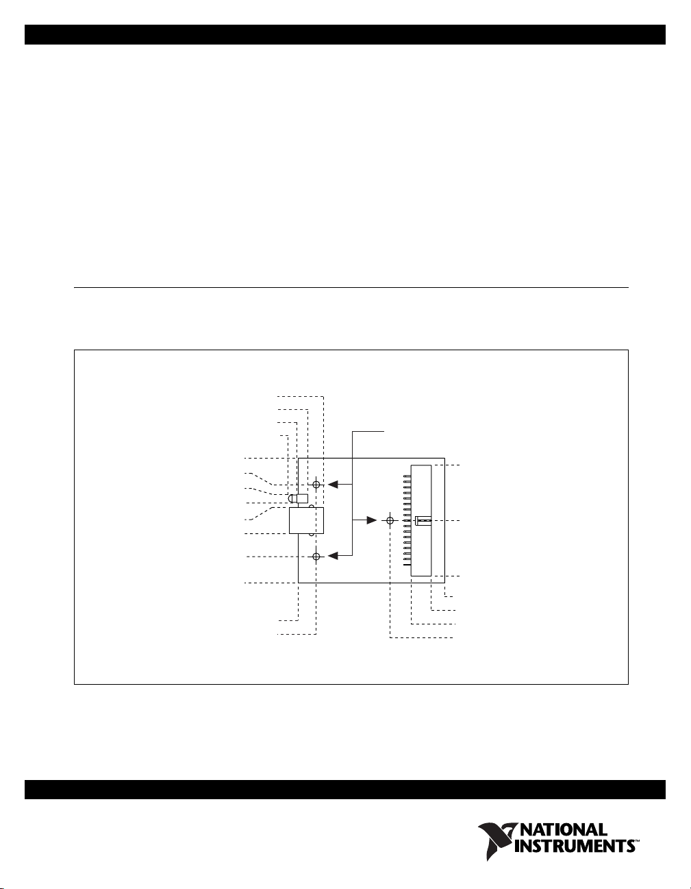
Dimensional Drawings
Figure 1 shows a top view of the USB-6501 OEM. Figure 2 shows the front
and rear dimensions.
0.45 in. (11.5 mm)
0.18 in. (4.5 mm)
–0.03 in. (–0.8 mm)
–0.18 in. (–4.6 mm)
2.26 in. (57.4 mm)
1.78 in. (45.2 mm)
1.61 in. (40.8 mm)
1.45 in. (36.7 mm)
1.37 in. (34.7 mm)
0.89 in. (22.7 mm)
0.48 in. (12.2 mm)
0.00 in. (0.0 mm)
0.00 in. (0.0 mm)
0.33 in. (8.3 mm)
0.125 in. (3.18 mm) Diameter
2.13 in. (54.1 mm)
1.13 in. (28.7 mm)
0.13 in. (3.3 mm)
2.65 in. (67.3 mm)
2.41 in. (61.2 mm)
2.04 in. (51.8 mm)
1.66 in. (42.2 mm)
Figure 1. USB-6501 OEM Dimensions (Top View)
Page 2
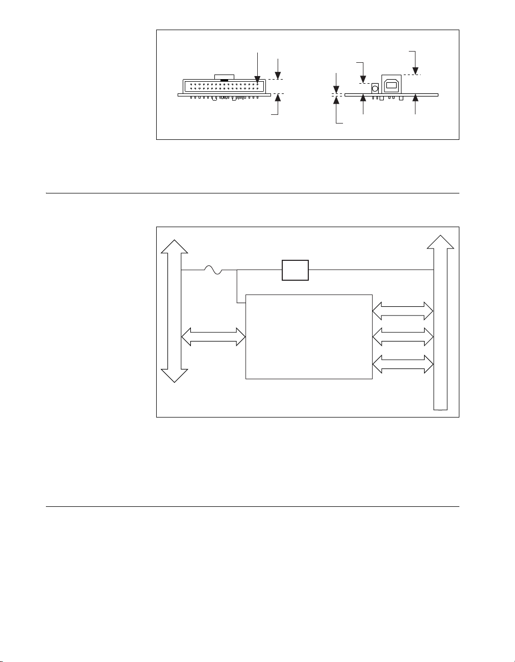
Block Diagram
Pin 1
0.25 in. (6.4 mm)
0.45 in. (11.5 mm)
0.34 in. (8.6 mm)
Figure 2. USB-6501 OEM Dimensions (Front and Rear Views)
Figure 3 shows key functional components of the USB-6501 OEM device.
Short Circuit Protection
Current Limiting Circuit
Vbus
USB
Full-Speed USB Interface
USB Microcontroller
0.06 in. (1.6 mm)
P2.<0..7>
P1.<0..7>
P0.<0..7>
+5 V
Digital I/O Terminal Block
Figure 3. Device Block Diagram
Refer to the Safety Guidelines section of this document for important safety
information.
Installing Software
To install the driver software for the USB-6501 OEM device, go to
ni.com/downloads, click the Drivers and Updates link, and select
Multifunction DAQ from the Product Line drop-down list. Next, select
the appropriate software, software version, and operating system.
USB-6501 OEM User Guide 2 ni.com
Page 3

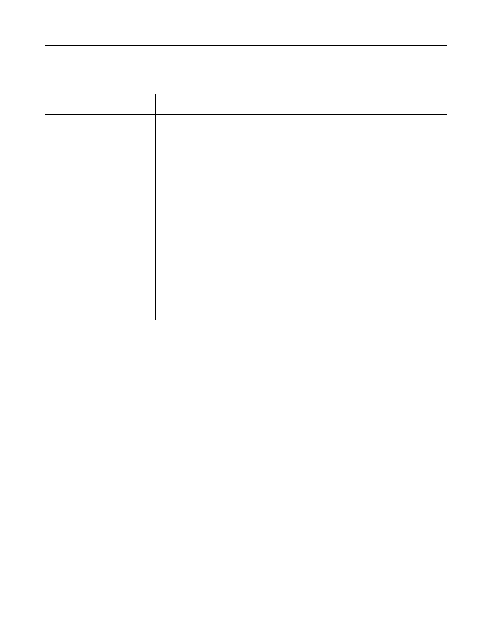
I/O Connector and Cable
Use any 34-pin female IDC (ribbon) cable to connect to the IDC connector
on the USB-6501 OEM device.
Table 1 lists the pin assignments and signal names for the IDC connector.
Table 1. Pin Assignments
Signal Pin Connector Pin Signal
P1.0 1 2 GND
P1.1 3 4 P2.0
P1.2 5 6 GND
P1.3 7 8 P2.1
Pin 1
P1.4 9 10 GND
P1.5 11 12 P2.2
P1.6 13 14 GND
P1.7 15 16 P2.3
P0.0 17 18 GND
Pin 2
P0.1 19 20 P2.4
P0.2 21 22 GND
P0.3 23 24 P2.5
Pin 33
Pin 34
P0.4 25 26 GND
P0.5 27 28 P2.6
P0.6 29 30 GND
P0.7 31 32 P2.7
+5V 33 34 +5V
© National Instruments Corporation 3 USB-6501 OEM User Guide
Page 4
Signal Descriptions
Table 2 describes the signals available on the I/O connectors.
Table 2. Signal Descriptions
Signal Name Direction Description
P0.<0..7>
P1.<0..7>
P2.<0..6>
P2.7 (CTR 0 SRC) Input or
+5 V Output +5 V—The voltage source provided by the USB host.
GND — Ground—The reference for the digital signals and the
Input or
Output
Output
Digital I/O Signals—You can individually configure
each signal as an input or output.
This pin is configurable as either a digital line or an
event counter.
Digital I/O Signal—As a digital line, this signal can be
used as an input or output.
CTR—As a counter, this signal can be used as an event
counter input source.
The voltage is nominally 5 V, but varies from system to
system.
+5 VDC supply.
Digital I/O
The USB-6501 OEM has 24 single-ended digital lines, P0.<0..7>,
P1.<0..7>, and P2.<0..7>, which comprise the three DIO ports. P2.7 can
also function as a 32-bit counter. Refer to the Event Counter section for
more information about the counter.
Static DIO
Each of the USB-6501 OEM DIO lines can be individually programmed as
a static DI or DO line. You can use static DIO lines to monitor or control
digital signals. All samples of static DI lines and updates of DO lines are
software-timed.
Source/Sink Information
The default configuration of the USB-6501 OEM DIO ports is open-drain,
allowing 5 V operation, with an onboard 4.7 kΩ pull-up resistor. An
external, user-provided, pull-up resistor can be added to increase the source
current drive up to a 8.5 mA limit per line, as shown in Figure 4.
USB-6501 OEM User Guide 4 ni.com
Page 5
+5 V
USB-6501 OEM DIO Box
Short Circuit Protection
Current Limiting Circuit
VBus
Re
External
Pull-up
Resistor
Rl
Load
Figure 4. Example of Connecting External User-Provided Resistor
P0.0
GND
A
Rp
4.7K Onboard Resistor
Por t Pad
Complete the following steps to determine the value of the user-provided
pull-up resistor:
1. Place an ammeter in series with the load.
2. Place a variable resistor between the digital output line and the +5 V.
3. Adjust the variable resistor until the ammeter current reads as the
intended current. The intended current must be less than 8.5 mA.
4. Remove the ammeter and variable resistor from your circuit.
5. Measure the resistance of the variable resistor. The measured
resistance is the ideal value of the pull-up resistor.
6. Select a static resistor value for your pull-up resistor that is greater than
or equal to the ideal resistance.
7. Reconnect the load circuit and the pull-up resistor.
Additionally, you can configure the USB-6501 OEM DIO ports as
push-pull.
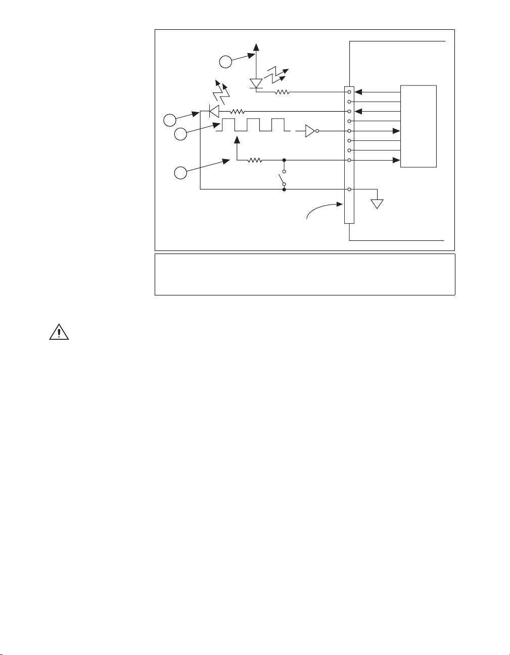
Digital I/O Circuitry
Figure 5 shows P0.<0..7> connected to example signals configured as
digital inputs and digital outputs. You can configure P1.<0..7> and
P2.<0..7> similarly. Refer to Figure 4 for some common examples of
connections of DIO lines with standard circuits.
© National Instruments Corporation 5 USB-6501 OEM User Guide
Page 6
+5 V
1
LED
LED
2
3
4
1 P0.0 configured as an open-drain digital output driving a LED
2 P0.2 configured as a push-pull digital output driving a LED
3 P0.4 configured as a digital input receiving a TTL signal from a gated inverter
4 P0.7 configured as a digital input receiving a 0 V or 5 V signal from a switch
+5 V
TTL Signal
Switch
GND
I/O Connector
P0.0
P0.1
P0.2
P0.3
P0.4
P0.5
P0.6
P0.7
Figure 5. Example of Connecting a Load
Caution
Exceeding the maximum input voltage ratings or maximum output ratings, which
are listed in the Specifications section, can damage the DAQ device and the computer.
National Instruments is not liable for any damage resulting from such signal connections.
I/O Protection
Each DIO signal is protected against overvoltage, undervoltage, and
overcurrent conditions, as well as ESD events. However, you should avoid
these fault conditions by using the following guidelines:
• If you configure a DIO line as an output, do not connect it to any
external signal source, ground signal, or power supply.
• If you configure a DIO line as an output, understand the current
requirements of the load connected to these signals. Do not exceed the
specified current output limits of the DAQ device.
• If you configure a DIO line as an input, do not drive the line with
voltages outside of its normal operating range.
• Treat the DAQ device as you would treat any static sensitive device.
Always properly ground yourself and the equipment when handling
the DAQ device or connecting to it.
USB-6501 OEM User Guide 6 ni.com
Page 7
Power-On States
At system startup and reset, the hardware sets all DIO lines to
high-impedance inputs. The DAQ device does not drive the signal high
or low. Each line has a weak pull-up resistor connected to it.
Event Counter
You can configure P2.7 as the source for a 32-bit counter. In this mode, the
device counts high to low transitions on P2.7. The counter can be armed
and disarmed and the count can be read or reset through software. Refer to
your software documentation for more information about counter
programming techniques.
+5 V Power Source
Caution When using the 5 V source, understand the current requirements of the load
connected. Do not exceed the specified current output limits of the USB Vbus.
The USB-6501 OEM supplies a nominal 5 V from two pins on the front
IDC connector. The voltage source is provided by the USB host. The
voltage is nominally 5 V, but varies from system to system. Refer to the
Specifications section for more information about USB bus power
specifications. This source can be used to power external components.
Note While the device is in USB suspend, the output is disabled.
Specifications
The following specifications are typical at 25 °C, unless otherwise noted.
Digital I/O
Number of lines
P0.<0..7>......................................... 8
P1.<0..7>......................................... 8
P2.<0..7>......................................... 8
Direction control .................................... Input or output,
software-selectable
Output driver type .................................. Push-pull or open-drain,
software selectable
© National Instruments Corporation 7 USB-6501 OEM User Guide
Page 8

Pull-up resistor........................................4.7 kΩ VBus (nominally 5 V)
Absolute voltage range ...........................–0.5 to 5.8 V with respect to GND
Power-on state ........................................Input (high impedance)
Digital logic levels
Level Min Max Units
Input
Input low voltage
Input high voltage
Input leakage current
Output
Output low voltage (I = 8.5 mA)
Output high voltage
Push-pull, I = –8.5 mA
Open-drain, I = –0.6 mA, nominal
Open-drain, I = –8.5 mA, with external pull-up resistor
Counter
Number of counters ................................1 (P2.7 can be configured as
–0.3
2.0
—
—
2.0
2.0
2.0
a counter)
0.8
5.8
50
0.8
3.5
5.0
—
V
V
µA
V
V
V
V
Resolution...............................................32 bits
Counter measurements ...........................Falling edge counting
Maximum input frequency .....................5 MHz
Minimum high pulse width.....................100 ns
Minimum low pulse width......................100 ns
Bus Interface
USB specification ...................................USB 2.0 full-speed (12 Mb/s)
External Voltage
+5 V output
Voltage ............................................4.10 V min, 5.25 V max
Current.............................................230 mA max
USB-6501 OEM User Guide 8 ni.com
Page 9

Power Requirements
USB
4.10 to 5.25 VDC............................ 80 mA typical, 500 mA max
USB Suspend .................................. 300 µA standby mode,
Physical Characteristics
Dimensions ............................................ 5.74 cm × 6.73 cm × 1.15 cm
I/O connectors ........................................ USB series B receptacle; 34-pin
Weight.................................................... 21 g (.74 oz)
Safety
Standards
The USB-6501 is designed to meet the requirements of the following
standards of safety for electrical equipment for measurement, control,
and laboratory use:
• IEC 61010-1, EN 61010-1
• UL 61010-1
• CAN/CSA-C22.2 No. 61010-1
500 µAmax
(2.26 in. × 2.65 in. × 0.45 in.)
IDC ribbon cable header
Note For UL and other safety certifications, refer to the product label, or visit
ni.com/certification, search by model number or product line, and click the
appropriate link in the Certification column.
Overvoltage Protection
Connect only voltages that are within these limits.
Channel-to-COM (one channel)............. ±30 V max,
Measurement Category I
Channels-to-COM
(one port, all channels)........................... ±8.9 V max,
Measurement Category I
Measurement Category I is for measurements performed on circuits not
directly connected to the electrical distribution system referred to as
MAINS voltage. MAINS is a hazardous live electrical supply system that
powers equipment. This category is for measurements of voltages from
© National Instruments Corporation 9 USB-6501 OEM User Guide
Page 10

Caution Do not use this module for connection to signals or for measurements within
Measurement Categories II, III, or IV.
Environmental
specially protected secondary circuits. Such voltage measurements include
signal levels, special equipment, limited-energy parts of equipment,
circuits powered by regulated low-voltage sources, and electronics.
Hazardous Locations
The USB-6501 is not certified for use in hazardous locations.
The USB-6501 device is intended for indoor use only.
Operating temperature
(IEC 60068-2-1 and IEC 60068-2-2)......0 to 55 °C
Operating humidity
(IEC 60068-2-56) ...................................10 to 90% RH, noncondensing
Maximum altitude...................................2,000 m (at 25 °C ambient
temperature)
Storage temperature
(IEC 60068-2-1 and IEC 60068-2-2)......–40 to 85 °C
Storage humidity
(IEC 60068-2-56) ..................................5 to 90% RH, noncondensing
Pollution Degree (IEC 60664) ................2
EMC/EMI ...............................................CE, C-Tick, and FCC Part 15
(Class A) Compliant
CE Compliance
The USB-6501 OEM device is intended to be used as part of a system. To
ensure that your system meets the appropriate CE Compliance regulations,
you must test the entire system.
This product meets the essential requirements of applicable European
Directives, as amended for CE marking, as follows:
Low-Voltage Directive (safety)..............73/23/EEC
Electromagnetic Compatibility
Directive (EMC) .....................................89/336/EEC
USB-6501 OEM User Guide 10 ni.com
Page 11

Note Refer to the Declaration of Conformity (DoC) for this product for any additional
regulatory compliance information. To obtain the DoC for this product, visit
ni.com/certification, search by model number or product line, and click the
appropriate link in the Certification column.
Safety Guidelines
Caution Operate the hardware only as described in these operating instructions.
The following section contains important safety information that you must
follow when installing and using the USB-6501 OEM device.
Do not operate the USB-6501 OEM device in a manner not specified in this
document. Misuse of the device can result in a hazard. You can compromise
the safety protection built into the device if the device is damaged in any
way. If the device is damaged, contact National Instruments for repair.
Do not substitute parts or modify the device except as described in this
document. Use the device only with the chassis, modules, accessories, and
cables specified in the installation instructions. You must have all covers
and filler panels installed during operation of the device.
Do not operate the device in an explosive atmosphere or where there may
be flammable gases or fumes. If you must operate the device in such an
environment, it must be in a suitably rated enclosure.
If you need to clean the device, use a dry cloth. Make sure that the device
is completely dry and free from contaminants before returning it to service.
Operate the device only at or below Pollution Degree 2. Pollution is foreign
matter in a solid, liquid, or gaseous state that can reduce dielectric strength
or surface resistivity. The following is a description of pollution degrees:
• Pollution Degree 1 means no pollution or only dry, nonconductive
pollution occurs. The pollution has no influence.
• Pollution Degree 2 means that only nonconductive pollution occurs in
most cases. Occasionally, however, a temporary conductivity caused
by condensation must be expected.
• Pollution Degree 3 means that conductive pollution occurs, or dry,
nonconductive pollution occurs that becomes conductive due to
condensation.
You must insulate signal connections for the maximum voltage for which
the device is rated. Do not exceed the maximum ratings for the device. Do
not install wiring while the device is live with electrical signals. Do not
remove or add connector blocks when power is connected to the system.
© National Instruments Corporation 11 USB-6501 OEM User Guide
Page 12

Avoid contact between your body and the connector block signal when hot
swapping modules. Remove power from signal lines before connecting
them to or disconnecting them from the device.
Operate the device at or below the Measurement Category I
circuits are subjected to working voltages
2
and transient stresses
1
. Measurement
(overvoltage) from the circuit to which they are connected during
measurement or test. Measurement categories establish standard impulse
withstand voltage levels that commonly occur in electrical distribution
systems. The following is a description of measurement categories:
• Measurement Category I is for measurements performed on circuits
not directly connected to the electrical distribution system referred to
as MAINS
3
voltage. This category is for measurements of voltages
from specially protected secondary circuits. Such voltage
measurements include signal levels, special equipment, limited-energy
parts of equipment, circuits powered by regulated low-voltage sources,
and electronics.
• Measurement Category II is for measurements performed on circuits
directly connected to the electrical distribution system. This category
refers to local-level electrical distribution, such as that provided by a
standard wall outlet (for example, 115 V for U.S. or 230 V for Europe).
Examples of Measurement Category II are measurements performed
on household appliances, portable tools, and similar E Series devices.
• Measurement Category III is for measurements performed in the
building installation at the distribution level. This category refers to
measurements on hard-wired equipment such as equipment in fixed
installations, distribution boards, and circuit breakers. Other examples
are wiring, including cables, bus-bars, junction boxes, switches,
socket-outlets in the fixed installation, and stationary motors with
permanent connections to fixed installations.
• Measurement Category IV is for measurements performed at the
primary electrical supply installation (<1,000 V). Examples include
electricity meters and measurements on primary overcurrent
protection devices and on ripple control units.
1
Measurement Category as defined in electrical safety standard IEC 61010-1. Measurement Category is also referred to as
Installation Category.
2
Working Voltage is the highest rms value of an AC or DC voltage that can occur across any particular insulation.
3
MAINS is defined as a hazardous live electrical supply system that powers equipment. Suitably rated measuring circuits may
be connected to the MAINS for measuring purposes.
USB-6501 OEM User Guide 12 ni.com
Page 13

Where to Go for Support
The National Instruments Web site is your complete resource for technical
support. At
troubleshooting and application development self-help resources to email
and phone assistance from NI Application Engineers.
National Instruments corporate headquarters is located at
11500 North Mopac Expressway, Austin, Texas, 78759-3504.
National Instruments also has offices located around the world to help
address your support needs. For telephone support in the United States,
create your service request at
instructions or dial 512 795 8248. For telephone support outside the United
States, contact your local branch office:
Australia 1800 300 800, Austria 43 0 662 45 79 90 0,
Belgium32027570020, Brazil551132623599,
Canada 800 433 3488, China 86 21 6555 7838,
Czech Republic 420 224 235 774, Denmark 45 45 76 26 00,
Finland3850972572511, France330148142424,
Germany 49 0 89 741 31 30, India 91 80 51190000,
Israel 972 0 3 6393737, Italy 39 02 413091, Japan 81 3 5472 2970,
Korea820234513400, Lebanon96101332828,
Malaysia 1800 887710, Mexico 01 800 010 0793,
Netherlands 31 0 348 433 466, New Zealand 0800 553 322,
Norway 47 0 66 90 76 60, Poland 48 22 3390150,
Portugal 351 210 311 210, Russia 7 095 783 68 51,
Singapore 1800 226 5886, Slovenia 386 3 425 4200,
South Africa 27 0 11 805 8197, Spain 34 91 640 0085,
Sweden460858789500, Switzerland41562005151,
Taiwan 886 02 2377 2222, Thailand 662 278 6777,
United Kingdom 44 0 1635 523545
ni.com/support you have access to everything from
ni.com/support and follow the calling
National Instruments, NI, ni.com, and LabVIEW are trademarks of National Instruments Corporation.
Refer to the Terms of Use section on ni.com/legal for more information about National
Instruments trademarks. Other product and company names mentioned herein are trademarks or trad e
names of their respective companies. For patents covering National Instruments products, refer to the
appropriate location: Help»Patents in your software, the patents.txt file on your CD, or
ni.com/patents.
© 2005 National Instruments Corporation. All rights reserved.
371594A-01 May05
 Loading...