

Page 1

NI Ultiboard
User Manual
NI Ultiboard User Manual
TM
May 2008
374488C-01
Page 2

Support
Worldwide Technical Support and Product Information
ni.com
National Instruments Corporate Headquarters
11500 North Mopac Expressway Austin, Texas 78759-3504 USA Tel: 512 683 0100
Worldwide Offices
Australia 1800 300 800, Austria 43 662 457990-0, Belgium 32 (0) 2 757 0020, Brazil 55 11 3262 3599,
Canada 800 433 3488, China 86 21 5050 9800, Czech Republic 420 224 235 774, Denmark 45 45 76 26 00,
Finland 358 (0) 9 725 72511, France 01 57 66 24 24, Germany 49 89 7413130, India 91 80 41190000,
Israel 972 3 6393737, Italy 39 02 41309277, Japan 0120-527196, Korea 82 02 3451 3400,
Lebanon 961 (0) 1 33 28 28, Malaysia 1800 887710, Mexico 01 800 010 0793, Netherlands 31 (0) 348 433 466,
New Zealand 0800 553 322, Norway 47 (0) 66 90 76 60, Poland 48 22 3390150, Portugal 351 210 311 210,
Russia 7 495 783 6851, Singapore 1800 226 5886, Slovenia 386 3 425 42 00, South Africa 27 0 11 805 8197,
Spain 34 91 640 0085, Sweden 46 (0) 8 587 895 00, Switzerland 41 56 2005151, Taiwan 886 02 2377 2222,
Thailand 662 278 6777, Turkey 90 212 279 3031, United Kingdom 44 (0) 1635 523545
For further support information, refer to the Technical Support and Professional Services appendix. To comment
on National Instruments documentation, refer to the National Instruments Web site at ni.com/info and enter
the info code feedback.
© 2006-2008 National Instruments Corporation. All rights reserved.
Page 3

Important Information
Warranty
The media on which you receive National Instruments software are warranted not to fail to execute programming instructions, due to defects
in materials and workmanship, for a period of 90 days from date of shipment, as evidenced by receipts or other documentation. National
Instruments will, at its option, repair or replace software media that do not execute programming instructions if National Instruments receives
notice of such defects during the warranty period. National Instruments does not warrant that the operation of the software shall be
uninterrupted or error free.
A Return Material Authorization (RMA) number must be obtained from the factory and clearly marked on the outside of the package before any
equipment will be accepted for warranty work. National Instruments will pay the shipping costs of returning to the owner parts which are covered by
warranty.
National Instruments believes that the information in this document is accurate. The document has been carefully reviewed for technical accuracy. In
the event that technical or typographical errors exist, National Instruments reserves the right to make changes to subsequent editions of this document
without prior notice to holders of this edition. The reader should consult National Instruments if errors are suspected. In no event shall National
Instruments be liable for any damages arising out of or related to this document or the information contained in it.
E
XCEPT AS SPECIFIED HEREIN, NATIONAL INSTRUMENTS MAKES NO WARRANTIES, EXPRESS OR IMPLIED, AND SPECIFICALLY DISCLAIMS ANY WARRANTY OF
MERCHANTABILITY OR FITNESS FOR A PARTICULAR PURPOSE. CUSTOMER’S RIGHT TO RECOVER DAMAGES CAUSED BY FAULT OR NEGLIGENCE ON THE PART OF NATIONAL
I
NSTRUMENTS SHALL BE LIMITED TO THE AMOUNT THERETOFORE PAID BY THE CUSTOMER. NATIONAL INSTRUMENTS WILL NOT BE LIABLE FOR DAMAGES RESULTING
FROM LOSS OF DATA, PROFITS, USE OF PRODUCTS, OR INCIDENTAL OR CONSEQUENTIAL DAMAGES, EVEN IF ADVISED OF THE POSSIBILITY THEREOF. This limitation of
the liability of National Instruments will apply regardless of the form of action, whether in contract or tort, including negligence. Any action against
National Instruments must be brought within one year after the cause of action accrues. National Instruments shall not be liable for any delay in
performance due to causes beyond its reasonable control. The warranty provided herein does not cover damages, defects, malfunctions, or service
failures caused by owner’s failure to follow the National Instruments installation, operation, or maintenance instructions; owner’s modification of the
product; owner’s abuse, misuse, or negligent acts; and power failure or surges, fire, flood, accident, actions of third parties, or other events outside
reasonable control.
Copyright
Under the copyright laws, this publication may not be reproduced or transmitted in any form, electronic or mechanical, including photocopying,
recording, storing in an information retrieval system, or translating, in whole or in part, without the prior written consent of National
Instruments Corporation.
National Instruments respects the intellectual property of others, and we ask our users to do the same. NI software is protected by copyright and other
intellectual property laws. Where NI software may be used to reproduce software or other materials belonging to others, you may use NI software only
to reproduce materials that you may reproduce in accordance with the terms of any applicable license or other legal restriction.
Anti-Grain Geometry - Version 2.4
Copyright (C) 2002-2004 Maxim Shemanarev (McSeem)
Permission to copy, use, modify, sell and distribute this software is granted provided this copyright notice appears in all copies. This software is
provided "as is" without express or implied warranty, and with no claim as to its suitability for any purpose.
Anti-Grain Geometry - Version 2.4
Copyright (C) 2002-2005 Maxim Shemanarev (McSeem)
1. Redistribution and use in source and binary forms, with or without modification, are permitted provided that the following conditions are met:
2. Redistributions of source code must retain the above copyright notice, this list of conditions and the following disclaimer.
3. Redistributions in binary form must reproduce the above copyright notice, this list of conditions and the following disclaimer in the documentation
and/or other materials provided with the distribution.
The name of the author may not be used to endorse or promote products derived from this software without specific prior written permission.
THIS SOFTWARE IS PROVIDED BY THE AUTHOR “AS IS” AND ANY EXPRESS OR IMPLIED WARRANTIES, INCLUDING, BUT NOT
LIMITED TO, THE IMPLIED WARRANTIES OF MERCHANTABILITY AND FITNESS FOR A PARTICULAR PURPOSE ARE
DISCLAIMED. IN NO EVENT SHALL THE AUTHOR BE LIABLE FOR ANY DIRECT, INDIRECT, INCIDENTAL, SPECIAL,
EXEMPLARY, OR CONSEQUENTIAL DAMAGES (INCLUDING, BUT NOT LIMITED TO, PROCUREMENT OF SUBSTITUTE GOODS OR
SERVICES; LOSS OF USE, DATA, OR PROFITS; OR BUSINESS INTERRUPTION) HOWEVER CAUSED AND ON ANY THEORY OF
LIABILITY, WHETHER IN CONTRACT, STRICT LIABILITY, OR TORT (INCLUDING NEGLIGENCE OR OTHERWISE) ARISING IN
ANY WAY OUT OF THE USE OF THIS SOFTWARE, EVEN IF ADVISED OF THE POSSIBILITY OF SUCH DAMAGE.
Trademarks
National Instruments, NI, ni.com, and LabVIEW are trademarks of National Instruments Corporation. Refer to the Terms of Use section
ni.com/legal for more information about National Instruments trademarks.
on
Ultiboard is a registered trademark and Multisim and Electronics Workbench are trademarks of Electronics Workbench.
Portions of this product obtained under license from Bartels Systems GmbH.
Other product and company names mentioned herein are trademarks or trade names of their respective companies.
Members of the National Instruments Alliance Partner Program are business entities independent from National Instruments and have no agency,
partnership, or joint-venture relationship with National Instruments.
Patents
For patents covering National Instruments products, refer to the appropriate location: Help»Patents in your software, the patents.txt file
on your media, or
ni.com/patents.
Page 4

WARNING REGARDING USE OF NATIONAL INSTRUMENTS PRODUCTS
(1) NATIONAL INSTRUMENTS PRODUCTS ARE NOT DESIGNED WITH COMPONENTS AND TESTING FOR A LEVEL OF
RELIABILITY SUITABLE FOR USE IN OR IN CONNECTION WITH SURGICAL IMPLANTS OR AS CRITICAL COMPONENTS IN
ANY LIFE SUPPORT SYSTEMS WHOSE FAILURE TO PERFORM CAN REASONABLY BE EXPECTED TO CAUSE SIGNIFICANT
INJURY TO A HUMAN.
(2) IN ANY APPLICATION, INCLUDING THE ABOVE, RELIABILITY OF OPERATION OF THE SOFTWARE PRODUCTS CAN BE
IMPAIRED BY ADVERSE FACTORS, INCLUDING BUT NOT LIMITED TO FLUCTUATIONS IN ELECTRICAL POWER SUPPLY,
COMPUTER HARDWARE MALFUNCTIONS, COMPUTER OPERATING SYSTEM SOFTWARE FITNESS, FITNESS OF COMPILERS
AND DEVELOPMENT SOFTWARE USED TO DEVELOP AN APPLICATION, INSTALLATION ERRORS, SOFTWARE AND HARDWARE
COMPATIBILITY PROBLEMS, MALFUNCTIONS OR FAILURES OF ELECTRONIC MONITORING OR CONTROL DEVICES,
TRANSIENT FAILURES OF ELECTRONIC SYSTEMS (HARDWARE AND/OR SOFTWARE), UNANTICIPATED USES OR MISUSES, OR
ERRORS ON THE PART OF THE USER OR APPLICATIONS DESIGNER (ADVERSE FACTORS SUCH AS THESE ARE HEREAFTER
COLLECTIVELY TERMED “SYSTEM FAILURES”). ANY APPLICATION WHERE A SYSTEM FAILURE WOULD CREATE A RISK OF
HARM TO PROPERTY OR PERSONS (INCLUDING THE RISK OF BODILY INJURY AND DEATH) SHOULD NOT BE RELIANT SOLELY
UPON ONE FORM OF ELECTRONIC SYSTEM DUE TO THE RISK OF SYSTEM FAILURE. TO AVOID DAMAGE, INJURY, OR DEATH,
THE USER OR APPLICATION DESIGNER MUST TAKE REASONABLY PRUDENT STEPS TO PROTECT AGAINST SYSTEM FAILURES,
INCLUDING BUT NOT LIMITED TO BACK-UP OR SHUT DOWN MECHANISMS. BECAUSE EACH END-USER SYSTEM IS
CUSTOMIZED AND DIFFERS FROM NATIONAL INSTRUMENTS' TESTING PLATFORMS AND BECAUSE A USER OR APPLICATION
DESIGNER MAY USE NATIONAL INSTRUMENTS PRODUCTS IN COMBINATION WITH OTHER PRODUCTS IN A MANNER NOT
EVALUATED OR CONTEMPLATED BY NATIONAL INSTRUMENTS, THE USER OR APPLICATION DESIGNER IS ULTIMATELY
RESPONSIBLE FOR VERIFYING AND VALIDATING THE SUITABILITY OF NATIONAL INSTRUMENTS PRODUCTS WHENEVER
NATIONAL INSTRUMENTS PRODUCTS ARE INCORPORATED IN A SYSTEM OR APPLICATION, INCLUDING, WITHOUT
LIMITATION, THE APPROPRIATE DESIGN, PROCESS AND SAFETY LEVEL OF SUCH SYSTEM OR APPLICATION.
Page 5
Conventions
The following conventions are used in this manual:
» The » symbol leads you through nested menu items and dialog box options
to a final action. The sequence File»Page Setup»Options directs you to
pull down the File menu, select the Page Setup item, and select Options
from the last dialog box.
This icon denotes a tip, which alerts you to advisory information.
This icon denotes a note, which alerts you to important information.
This icon denotes a caution, which advises you of precautions to take to
avoid injury, data loss, or a system crash.
bold Bold text denotes items that you must select or click in the software, such
as menu items and dialog box options. Bold text also denotes parameter
names.
italic Italic text denotes variables, emphasis, a cross-reference, or an introduction
to a key concept. Italic text also denotes text that is a placeholder for a word
or value that you must supply.
monospace Text in this font denotes text or characters that you should enter from the
keyboard, sections of code, programming examples, and syntax examples.
This font is also used for the proper names of disk drives, paths, directories,
programs, subprograms, subroutines, device names, functions, operations,
variables, filenames, and extensions.
Page 6

Contents
Chapter 1
User Interface
Introduction to the Ultiboard Interface ..........................................................................1-1
Toolbars .........................................................................................................................1-1
Standard Toolbar .............................................................................................1-1
View Toolbar...................................................................................................1-3
Main Toolbar ...................................................................................................1-4
Select Toolbar..................................................................................................1-5
Draw Settings Toolbar.....................................................................................1-6
Edit Toolbar.....................................................................................................1-7
Align Toolbar ..................................................................................................1-8
Place Toolbar...................................................................................................1-9
Wizard Toolbar................................................................................................1-12
Autoroute Toolbar ...........................................................................................1-12
Setting Preferences ........................................................................................................1-13
General Tab .....................................................................................................1-13
Paths Tab .........................................................................................................1-14
Colors Tab .......................................................................................................1-15
PCB Design Tab ..............................................................................................1-15
Dimensions Tab...............................................................................................1-18
3D Options Tab ...............................................................................................1-19
Setting PCB Properties ..................................................................................................1-20
Attributes Tab..................................................................................................1-20
Grid & Units Tab.............................................................................................1-20
Copper Layers Tab ..........................................................................................1-21
Pads/Vias Tab..................................................................................................1-22
General Layers Tab .........................................................................................1-24
Design Rules Tab ............................................................................................1-25
Setting Favorite Layers....................................................................................1-26
Design Toolbox..............................................................................................................1-27
Birds Eye View..............................................................................................................1-28
Spreadsheet View ..........................................................................................................1-29
Spreadsheet View: DRC Tab...........................................................................1-30
Spreadsheet View: Results Tab.......................................................................1-32
Spreadsheet View: Parts Tab...........................................................................1-33
Spreadsheet View: Part Groups Tab................................................................1-34
Spreadsheet View: Nets Tab ...........................................................................1-35
Spreadsheet View: Nets Groups Tab...............................................................1-38
Filter Manager...................................................................................1-31
© National Instruments Corporation vii NI Ultiboard User Manual
Page 7

Contents
Spreadsheet View: SMT Pads Tab.................................................................. 1-39
Spreadsheet View: THT Pads Tab .................................................................. 1-40
Spreadsheet View: Vias Tab ........................................................................... 1-42
Spreadsheet View: Copper Areas Tab ............................................................ 1-43
Spreadsheet View: Keep-ins/Keep-outs Tab .................................................. 1-44
Spreadsheet View: PCB Layers Tab............................................................... 1-45
Spreadsheet View: Parts Position Tab ............................................................ 1-45
Spreadsheet View: Statistics Tab.................................................................... 1-46
Customizing the Interface.............................................................................................. 1-46
Commands Tab ............................................................................................... 1-47
Toolbars Tab ................................................................................................... 1-47
Keyboard Tab.................................................................................................. 1-48
Menu Tab ........................................................................................................ 1-48
Options Tab..................................................................................................... 1-49
Customization of Pop-up Menus..................................................................... 1-49
Chapter 2
Beginning a Design
About Designs and Projects........................................................................................... 2-1
Creating a Project .......................................................................................................... 2-1
Creating a Design .......................................................................................................... 2-2
Creating a Design from a Netlist File............................................................................ 2-2
Working with Projects................................................................................................... 2-4
Opening an Existing File ............................................................................................... 2-5
Saving and Closing........................................................................................................ 2-5
Saving Technology Specifications from a Design ........................................................ 2-6
Loading Technology Files............................................................................................. 2-6
Selecting and Unselecting Elements ............................................................................. 2-7
Place and Select Modes ................................................................................................. 2-8
Searching for Design Elements ..................................................................................... 2-8
Options for Viewing the Design.................................................................................... 2-9
Using the Full Screen...................................................................................... 2-9
Magnifying and Shrinking the View............................................................... 2-10
Refreshing the Design..................................................................................... 2-11
Tool-tip Label ................................................................................................. 2-11
Chapter 3
Setting Up a Design
Working with Layers.....................................................................................................3-1
Defining Copper Layers.................................................................................. 3-1
Accessing Layers ............................................................................................ 3-3
NI Ultiboard User Manual viii ni.com
Page 8

Working with the Board Outline ...................................................................................3-5
Using the Drawing Tools to Create a Board Outline ......................................3-5
Importing a DXF File ......................................................................................3-6
Using a Pre-Defined Board Outline ................................................................3-6
Using the Board Wizard ..................................................................................3-7
Setting the Board’s Reference Point..............................................................................3-8
Enter coordinate dialog box.............................................................................3-9
Design Rule Errors.........................................................................................................3-10
Working with the Group Editor .....................................................................................3-11
Add Group dialog box.....................................................................................3-11
Working with Net Groups ...............................................................................3-12
Working with Part Groups...............................................................................3-13
Working with Bus Groups...............................................................................3-15
Working with Differential Pairs ......................................................................3-17
Change Group Settings dialog box..................................................................3-18
Chapter 4
Working with Parts
Placing Parts ..................................................................................................................4-1
Dragging Parts from Outside the Board Outline .............................................4-1
Using the Parts Tab in the Spreadsheet View .................................................4-2
Tools to Assist Part Placement........................................................................4-5
Unplacing Parts ...............................................................................................4-15
Viewing and Editing Properties .....................................................................................4-15
Attributes .........................................................................................................4-15
Viewing and Editing Part Properties ...............................................................4-17
Viewing and Editing Attributes.......................................................................4-19
Viewing and Editing Shape/Graphics Properties ............................................4-20
Contents
Net Group Settings............................................................................3-19
Part Group Settings ...........................................................................3-19
Differential Pair Settings...................................................................3-20
Using the Parts Tab to Place Parts ....................................................4-3
Using the Parts Tab for Other Functions ..........................................4-4
Working with Ratsnests ....................................................................4-5
Working with Force Vectors.............................................................4-6
Dragging Parts...................................................................................4-7
Shoving Parts ....................................................................................4-7
Using Ruler Bars and Guides............................................................4-10
Orienting Parts ..................................................................................4-11
Aligning Shapes and Parts ................................................................4-11
Spacing Shapes and Parts..................................................................4-12
Placing a Group Array Box............................................................... 4-12
Replicating a Group ..........................................................................4-14
© National Instruments Corporation ix NI Ultiboard User Manual
Page 9

Contents
Placing Other Elements ................................................................................................. 4-20
Placing Mounting Holes and Connectors........................................................ 4-21
Placing Holes .................................................................................................. 4-21
Placing Shapes and Graphics .......................................................................... 4-21
Working with Jumpers .................................................................................... 4-23
Placing Jumpers................................................................................ 4-23
Viewing and Editing Jumper Properties ........................................... 4-23
Working with Test Points ............................................................................... 4-24
Placing Test Points ........................................................................... 4-24
Viewing and Editing Test Point Properties ...................................... 4-25
Working with Dimensions ..............................................................................4-25
Placing Dimensions .......................................................................... 4-25
Viewing and Editing Dimension Properties .....................................4-26
Placing Parts from the Database.................................................................................... 4-27
Editing Parts and Shapes ............................................................................................... 4-29
Editing a Placed Part (In-Place Edit) .............................................................. 4-29
Editing a Polygon............................................................................................ 4-30
Viewing and Editing Through Hole Pin Properties ........................................ 4-31
Viewing and Editing SMT Pin Properties....................................................... 4-33
Searching For and Replacing Parts................................................................................ 4-34
Searching for Parts in Open Designs .............................................................. 4-34
Locating a Part in a Design............................................................................. 4-34
Replacing Parts ............................................................................................... 4-35
Cross-probing ................................................................................................................ 4-35
Creating New Parts........................................................................................................ 4-35
Using the Database Manager to Create a Part................................................. 4-35
Using the Part Wizard to Create a Part ........................................................... 4-36
Managing the Database ................................................................................................. 4-41
Working with Database Categories................................................................. 4-43
Adding Parts to the Database .......................................................................... 4-44
Adding Parts using the Database Manager....................................... 4-45
Adding Parts using the Add Selection to Database Command ........ 4-45
Merging and Converting Databases .............................................................................. 4-46
Merging Databases.......................................................................................... 4-46
Converting Databases ..................................................................................... 4-47
Chapter 5
Working with Traces and Copper
Placing Traces ............................................................................................................... 5-1
Working with Traces....................................................................................... 5-2
Placing a Trace: Manual Method .................................................................... 5-2
Placing a Trace: Follow-me Method............................................................... 5-3
Placing a Trace: Connection Machine Method............................................... 5-4
NI Ultiboard User Manual x ni.com
Page 10

Contents
Placing a Bus ...................................................................................................5-5
Working with Density Bars.............................................................................5-6
Working with Keep-in/Keep-out Areas...........................................................5-7
Placing Keep-in/Keep-out Areas ......................................................5-7
Viewing and Editing Keep-in/Keep-out Properties ..........................5-7
Equi-Spacing Traces........................................................................................5-9
Deleting a Trace ..............................................................................................5-9
Working with Other Copper Elements ..........................................................................5-10
Placing Copper Areas ......................................................................................5-10
Placing Powerplanes........................................................................................5-11
Splitting Copper...............................................................................................5-11
Converting a Copper Shape to an Area ...........................................................5-12
Deleting All Copper ........................................................................................5-12
Adding and Removing Teardrops ...................................................................5-13
Viewing and Editing Copper Properties ........................................................................5-13
Working with Vias.........................................................................................................5-15
Placing Vias.....................................................................................................5-15
Viewing and Editing Via Properties................................................................5-16
Placing SMD Fanouts ....................................................................................................5-18
Working with Nets.........................................................................................................5-19
Using the Nets Tab ..........................................................................................5-19
Using the Netlist Editor...................................................................................5-20
Adding a Net .....................................................................................5-21
Renaming a Net.................................................................................5-25
Deleting a Net ...................................................................................5-25
Deleting a Pin from a Net .................................................................5-26
Setting Net Widths ............................................................................5-26
Setting High Speed Parameters.........................................................5-26
Setting Miscellaneous Net Parameters..............................................5-27
Setting Group Parameters .................................................................5-27
Setting Via Parameters......................................................................5-28
Highlighting a Net ...........................................................................................5-28
Shielding Nets .................................................................................................5-28
Net Bridges......................................................................................................5-30
Creating a Net Bridge .......................................................................5-30
Placing a Net Bridge .........................................................................5-32
Copying a Copper Route .................................................................................5-33
Swapping Pins and Gates...............................................................................................5-34
Swapping Pins .................................................................................................5-34
Swapping Gates ...............................................................................................5-35
Automatic Pin/Gate Swapping ........................................................................5-38
Real-Time Pin/Gate Swapping........................................................................5-39
© National Instruments Corporation xi NI Ultiboard User Manual
Page 11

Contents
Chapter 6
PCB Calculators
PCB Transmission Line Calculator............................................................................... 6-1
Microstrip Trace Calculations......................................................................... 6-2
Embedded Microstrip Trace Calculations....................................................... 6-3
Centered Stripline Trace Calculations ............................................................ 6-4
Asymmetric Stripline Trace Calculations ....................................................... 6-5
Dual Stripline Trace Calculations ................................................................... 6-6
PCB Differential Impedance Calculator........................................................................ 6-7
Microstrip Calculations................................................................................... 6-8
Embedded Microstrip Calculations................................................................. 6-9
Centered Stripline Calculations ...................................................................... 6-11
Asymmetric Stripline Calculations ................................................................. 6-12
Chapter 7
Autorouting and Autoplacement
Autoroute Menu Items................................................................................................... 7-1
Autoplacement of Parts ................................................................................................. 7-2
Pre-Placing Parts ............................................................................................. 7-2
Understanding How the Autoplacer Works .................................................... 7-2
Running the Autoplacer .................................................................................. 7-3
Controlling the Autoplacer ............................................................................. 7-3
Strategies to Achieve Better Part Placement................................................... 7-5
Autorouting.................................................................................................................... 7-6
Understanding How the Autorouter Works .................................................... 7-6
Understanding the Four Fundamental Routing Functions .............................. 7-7
Router Preprocessing........................................................................ 7-7
Initial Routing................................................................................... 7-7
Rip-up and Retry Routing................................................................. 7-7
Optimization ..................................................................................... 7-8
Routing Selected Parts and Nets ..................................................................... 7-8
Running the Autorouter .................................................................................. 7-8
Interactivity....................................................................................... 7-9
Autorouting buses ........................................................................................... 7-9
Placing Automatic Test Points........................................................................ 7-10
Controlling the Routing Functions.................................................................. 7-11
Routing Options: General Tab..........................................................7-11
Routing Options: Cost Factors Tab .................................................. 7-12
Routing Options: Rip-Up Tab ..........................................................7-14
Routing Options: Optimization Tab ................................................. 7-15
Routing Options: Bus Autorouting Tab............................................7-16
Strategies to Achieve Better Routing Results ................................................. 7-17
NI Ultiboard User Manual xii ni.com
Page 12

Chapter 8
Preparing for Manufacturing/Assembly
Placing and Editing Text................................................................................................8-1
Capturing Screen Area...................................................................................................8-2
Placing a Comment........................................................................................................8-3
Renumbering Parts.........................................................................................................8-5
Backannotation to Multisim...........................................................................................8-6
Mitering Corners............................................................................................................8-6
Manually Re-Running the Design Rules and Netlist Check..........................................8-8
Cleaning up the Board ...................................................................................................8-8
Deleting Open Trace Ends...............................................................................8-8
Deleting Unused Vias......................................................................................8-8
Exporting a File .............................................................................................................8-8
Using Export Settings......................................................................................8-9
Viewing and Editing Export Properties...........................................................8-10
Setting Gerber Properties ..................................................................8-10
Setting DXF Properties .....................................................................8-11
Setting NC Drill Properties ...............................................................8-11
Working with SVG Properties ..........................................................8-11
Working with other Properties..........................................................8-12
Exporting the Desired File...............................................................................8-14
Printing your Design......................................................................................................8-14
Previewing the Printed Design .....................................................................................8-15
Contents
Chapter 9
Viewing Designs in 3D
Viewing the Board in 3D ..............................................................................................9-1
Manipulating the 3D View ............................................................................................9-2
Controlling the Elements Viewed in 3D .........................................................9-3
Showing an Object’s Height............................................................................9-4
Internal View ...................................................................................................9-4
Exporting to 3D DXF ....................................................................................................9-5
Exporting to 3D IGES....................................................................................................9-6
Chapter 10
Using Mechanical CAD
Creating Mechanical CAD Projects...............................................................................10-1
Creating Mechanical CAD Design Files .......................................................................10-2
Importing a DXF File ......................................................................................10-3
Setting Mechanical CAD Properties and Options .........................................................10-3
Setting Mechanical CAD Properties ...............................................................10-3
© National Instruments Corporation xiii NI Ultiboard User Manual
Page 13

Contents
Setting Mechanical CAD Colors..................................................................... 10-3
Controlling Workspace Elements for Mechanical CAD................................. 10-4
Setting Paths for Mechanical CAD................................................................. 10-5
Setting Mechanical CAD Dimensions ........................................................... 10-5
Appendix A
Menus and Commands
File Menu.......................................................................................................................A-1
File»New Design............................................................................................. A-1
File»New Project............................................................................................. A-1
File»Open........................................................................................................ A-1
File»Open Samples ......................................................................................... A-1
File»Save......................................................................................................... A-1
File»Save As ................................................................................................... A-2
File»Save All................................................................................................... A-2
File»Close ....................................................................................................... A-2
File»Close Project ........................................................................................... A-2
File»Close All ................................................................................................. A-2
File»Import...................................................................................................... A-2
File»Export...................................................................................................... A-2
File»Save Technology..................................................................................... A-2
File»Load Technology .................................................................................... A-2
File»Print Setup............................................................................................... A-3
File»Print Preview........................................................................................... A-3
File»Print......................................................................................................... A-3
File»Recent Designs ....................................................................................... A-3
File»Exit.......................................................................................................... A-3
Edit Menu ...................................................................................................................... A-3
Edit»Undo ....................................................................................................... A-3
Edit»Redo........................................................................................................ A-3
Edit»Cut .......................................................................................................... A-4
Edit»Copy ....................................................................................................... A-4
Edit»Paste........................................................................................................A-4
Edit»Paste Special........................................................................................... A-4
Edit»Delete...................................................................................................... A-4
Edit»Copper Delete......................................................................................... A-4
Edit»Find......................................................................................................... A-5
Edit»Select All ................................................................................................A-5
Edit»Select Entire Trace ................................................................................. A-5
Edit»Group Selection...................................................................................... A-5
Edit»Ungroup Selection..................................................................................A-5
Edit»Lock........................................................................................................ A-5
Edit»Unlock .................................................................................................... A-5
NI Ultiboard User Manual xiv ni.com
Page 14

Contents
Edit»Selection Filter........................................................................................A-6
Edit»Orientation ..............................................................................................A-6
Edit»Align .......................................................................................................A-6
Edit»Vertex......................................................................................................A-7
Edit»In-Place Part Edit ....................................................................................A-7
Edit»Properties ................................................................................................A-7
View Menu ....................................................................................................................A-8
View»Full Screen ............................................................................................A-8
View»Redraw Screen ......................................................................................A-8
View»Zoom In.................................................................................................A-8
View»Zoom Out..............................................................................................A-8
View»Zoom Window ......................................................................................A-8
View»Zoom Full .............................................................................................A-8
View»Clearances.............................................................................................A-8
View»Grid .......................................................................................................A-8
View»Ruler Bars .............................................................................................A-9
View»Status Bar..............................................................................................A-9
View»Density Bars..........................................................................................A-9
View»Birds Eye...............................................................................................A-9
View»Design Toolbox.....................................................................................A-9
View»Spreadsheet View .................................................................................A-9
View»3D Preview ...........................................................................................A-9
View»Toolbars ................................................................................................A-9
Place Menu ....................................................................................................................A-10
Place»From Database ......................................................................................A-10
Place»Line .......................................................................................................A-10
Place»Select.....................................................................................................A-10
Place»Follow-me.............................................................................................A-11
Place»Connection Machine .............................................................................A-11
Place»Shape.....................................................................................................A-11
Place»Dimension.............................................................................................A-11
Place»Graphic»Line ........................................................................................A-11
Place»Graphic»Arc..........................................................................................A-12
Place»Graphic»Bezier .....................................................................................A-12
Place»Graphic»Picture ....................................................................................A-12
Place»Graphic»Text .......................................................................................A-12
Place»Copper Area..........................................................................................A-12
Place»Powerplane............................................................................................A-12
Place»Bus ........................................................................................................A-12
Place»Keep-in/Keep-out Area.........................................................................A-13
Place»Group Array Box ..................................................................................A-13
Place»Pins........................................................................................................A-13
Place»Via.........................................................................................................A-13
Place»Test Point ..............................................................................................A-13
© National Instruments Corporation xv NI Ultiboard User Manual
Page 15

Contents
Place»Jumper .................................................................................................. A-13
Place»Net Bridge ............................................................................................ A-13
Place»Hole ...................................................................................................... A-13
Place»Automatic Test Points .......................................................................... A-14
Place»Unplace Parts........................................................................................ A-14
Place»Comment .............................................................................................. A-14
Design Menu ................................................................................................................. A-14
Design»Netlist & DRC Check ........................................................................ A-14
Design»Connectivity Check ........................................................................... A-14
Design»Polygon Splitter ................................................................................. A-15
Design»Shape to Area..................................................................................... A-15
Design»Swap Pins........................................................................................... A-15
Design»Swap Gates ........................................................................................ A-15
Design»Automatic Pin Gate Swap.................................................................. A-15
Design»Part Shoving....................................................................................... A-15
Design»Set Reference Point............................................................................ A-15
Design»Shield Nets......................................................................................... A-15
Design»Fanout SMD....................................................................................... A-16
Design»Add Teardrops ................................................................................... A-16
Design»Corner Mitering ................................................................................. A-16
Design»Remove Unused Vias ........................................................................ A-16
Design»Group Replica Place ..........................................................................A-16
Design»Copy Route ........................................................................................ A-16
Design»Highlight Selected Net....................................................................... A-16
Tools Menu....................................................................................................................A-17
Tools»Board Wizard ....................................................................................... A-17
Tools»Part Wizard .......................................................................................... A-17
Tools»Database»Database Manager ............................................................... A-17
Tools»Database»Add Selection to Database .................................................. A-17
Tools»Database»Set Database Password........................................................ A-17
Tools»Database»Merge Database...................................................................A-17
Tools»Database»Convert Database ................................................................ A-18
Tools»PCB Transmission Line Calculator ..................................................... A-18
Tools»PCB Differential Impedance Calculator .............................................. A-18
Tools»Netlist Editor........................................................................................ A-18
Tools»Group Editor ........................................................................................ A-18
Tools»Quick Layer Toggle ............................................................................. A-18
Tools»Renumber Parts.................................................................................... A-18
Tools»Equi-space Traces ................................................................................ A-19
Tools»Change Shape....................................................................................... A-19
Tools»Update Shapes...................................................................................... A-19
Tools»Highlight Selection in Multisim........................................................... A-19
Tools»Capture Screen Area ............................................................................ A-19
Tools»View 3D ...............................................................................................A-19
NI Ultiboard User Manual xvi ni.com
Page 16

Contents
Tools»View 3D Position .................................................................................A-19
Tools»Show or Hide Height............................................................................A-19
Options Menu ................................................................................................................A-20
Options»Global Preferences............................................................................A-20
Options»PCB Properties..................................................................................A-20
Options»Customize User Interface..................................................................A-20
Autoroute Menu.............................................................................................................A-20
Window Menu ...............................................................................................................A-20
Window»New Window ...................................................................................A-20
Window»Close ................................................................................................A-20
Window»Close All ..........................................................................................A-21
Window»Cascade ............................................................................................A-21
Window»Tile Horizontal.................................................................................A-21
Window»Tile Vertical .....................................................................................A-21
Window»Windows ..........................................................................................A-21
Window»<open designs> ................................................................................A-21
Help Menu .....................................................................................................................A-21
Help»Ultiboard Help .......................................................................................A-21
Help»Release Notes.........................................................................................A-21
Help»Patents....................................................................................................A-21
Help»File Information .....................................................................................A-21
Help»About Ultiboard .....................................................................................A-22
Context Menus...............................................................................................................A-22
Select Menu .....................................................................................................A-22
Right-drag Menu .............................................................................................A-24
Place Trace Menu ............................................................................................A-24
Appendix B
Archiving Data
Backing up the Corporate Database...............................................................................B-1
Backing up the User Database and Configuration files .................................................B-2
Appendix C
Technical Support and Professional Services
Glossary
Index
© National Instruments Corporation xvii NI Ultiboard User Manual
Page 17

User Interface
The following sections explain the basic components of the Ultiboard
Graphical User Interface (GUI) and show how to set up user preferences
and PCB properties.
Some of the described features may not be available in your edition of
Ultiboard. Refer to the NI Circuit Design Suite Release Notes for a list of
the features in your edition.
Introduction to the Ultiboard Interface
Ultiboard is the PCB layout application of National Instruments Circuit
Design Suite, a suite of EDA (Electronics Design Automation) tools that
assists you in carrying out the major steps in the circuit design flow.
Ultiboard is used to design printed circuit boards, perform certain basic
mechanical CAD operations, and prepare them for manufacturing. It also
provides automated parts placement and layout.
Note For more information on the Ultiboard interface, and information on the other
components of NI Circuit Design Suite, refer to Getting Started with NI Circuit Design
Suite.
1
Toolbars
The toolbars provide a quick, convenient way for you to access the most
common Ultiboard functions. You can toggle toolbars on and off using the
View»Toolbars menu.
Standard Toolbar
The Standard toolbar contains buttons for basic editing functions, and
appears by default when you run Ultiboard. The Standard toolbar buttons
are described in the table below.
© National Instruments Corporation 1-1 NI Ultiboard User Manual
Page 18
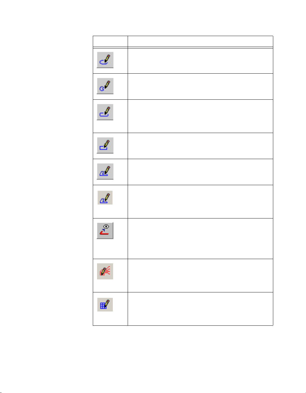
Chapter 1 User Interface
Button Description
New File button. Creates a new project (if none are
currently open) or a new design if a project is currently
open. Refer to the Creating a Project and Creating a
Design sections of Chapter 2, Beginning a Design, for
more information.
Open File button. Opens an existing project. Refer to the
Opening an Existing File section of Chapter 2, Beginning
a Design, for more information.
Open Sample button. Opens the samples folder.
Save File button. Saves the active design to its current
name and directory. Refer to the Saving and Closing
section of Chapter 2, Beginning a Design, for more
information.
Print button. Displays the Print dialog. Refer to the
Printing your Design section of Chapter 8, Preparing for
Manufacturing/Assembly, for more information.
Cut button. Cuts the selected element from the design and
places it on the Windows Clipboard.
Copy button. Copies the selected element from the design
and places it on the Windows Clipboard.
Paste button. Pastes the element from the Windows
Clipboard to the design.
Undo button. Undoes the last action.
Redo button. Redoes the last action (used after undoing).
NI Ultiboard User Manual 1-2 ni.com
Page 19
View Toolbar
Chapter 1 User Interface
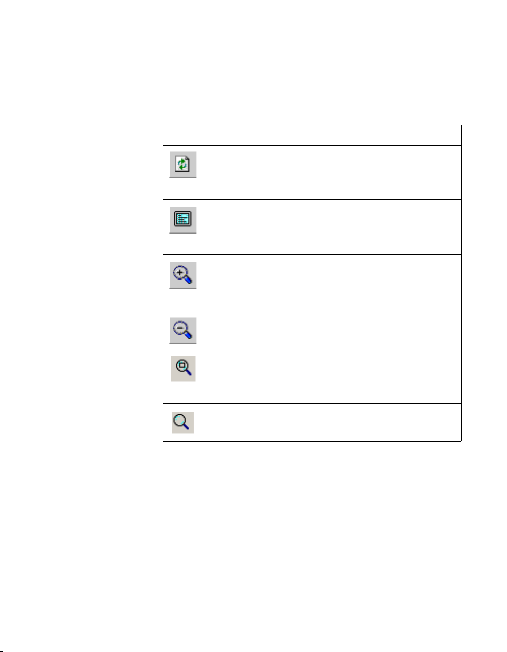
The View toolbar contains buttons for modifying the way the screen is
displayed, and appears by default when you run Ultiboard. The View
toolbar buttons are explained in the table below.
Button Description
Redraw the Screen button. Redraws the currently active
design workspace. Refer to the Refreshing the Design
section of Chapter 2, Beginning a Design, for more
information.
Toggle Full Screen button. Adjusts the size of the
workspace so it displays the entire design. Refer to the
Using the Full Screen section of of Chapter 2, Beginning
a Design, for more information.
Zoom In button. Zooms in on the design, providing a
closer view. Refer to the Magnifying and Shrinking the
View section of Chapter 2, Beginning a Design, for more
information.
Zoom Out button. Zooms out on the design, providing a
broader view.
Zoom Window button. Magnifies a selected part of the
design. Refer to the Magnifying and Shrinking the View
section of Chapter 2, Beginning a Design, for more
information.
Zoom Bounds button. Shows the entire design, including
objects that are outside of the board outline.
© National Instruments Corporation 1-3 NI Ultiboard User Manual
Page 20
Chapter 1 User Interface
Main Toolbar
The Main toolbar contains buttons for common board design functions. Its
buttons are described in the table below.
Button Description
Select button. De-activates any selected mode (for
example, for placing traces) and allows you to select an
element on the board.
Show or Hide Design Toolbox button. Shows or hides
the Design Toolbox. Refer to the Design Toolbox section
for more information.
Show or Hide Spreadsheet button. Shows or hides the
Spreadsheet View. Refer to the Spreadsheet View
section for more information.
Database Manager button. Displays the Database
Manager. Refer to the Managing the Database section of
Chapter 4, Working with Parts, for more information.
Board Wizard button. Launches the Board Wizard.
Refer to the Using the Board Wizard section of Chapter 3,
Setting Up a Design, for more information.
Part Wizard button. Starts the Part Wizard. Refer to the
Using the Part Wizard to Create a Part section of
Chapter 4, Working with Parts, for more information.
Place Part from Database button. Allows you to browse
the database for a part to place. Refer to the Placing Parts
from the Database section of Chapter 4, Working with
Parts, for more information.
Place Line button. Places a straight line on the design (or
places a trace, if the active layer is a copper one). Refer to
the Placing Shapes and Graphics section of Chapter 4,
Working with Parts, and the Placing a Trace: Manual
Method section of Chapter 5, Working with Traces and
Copper, for more information.
Follow-me button. Places a follow-me trace. Refer to the
Placing a Trace: Follow-me Method section of
Chapter 5, Working with Traces and Copper, for more
information.
NI Ultiboard User Manual 1-4 ni.com
Page 21
Button Description
Place Via button. Places a via on the design. Refer to the
Working with Vias section of Chapter 5, Working with
Traces and Copper, for more information.
Place Copper Area button. Places a copper area on the
design.
Create Power Plane button. Places a powerplane on the
design. Refer to the Placing Powerplanes section of
Chapter 5, Working with Traces and Copper, for more
information.
Design Rule Check button. Runs the Design Rule
Check and places results in the Results tab.
Place Text button. Places text on the design. Refer to the
Placing and Editing Text section of Chapter 8, Preparing
for Manufacturing/Assembly, for more information.
Show 3D button. Displays the current design in three
dimensions. Refer to the section of Chapter 9, Viewing
Designs in 3D, for more information.
Chapter 1 User Interface
Help button. Displays the helpfile contents page.
Select Toolbar
The Select toolbar contains the functions used to control selection filters,
and appears by default when you run Ultiboard. Please note that all filters
are not available in all versions of Ultiboard. The Select toolbar buttons are
explained in the table below.
Button Description
Enable Selecting Parts button. Use to allow or prevent
selection of parts.
Enable Selecting Traces button. Use to allow or prevent
selection of traces.
© National Instruments Corporation 1-5 NI Ultiboard User Manual
Page 22
Chapter 1 User Interface
Button Description
Enable Selecting Copper Areas button. Use to allow or
prevent selection of copper areas.
Enable Selecting Vias button. Use to allow or prevent
selection of vias.
Enable Selecting Pads button. Use to allow or prevent
selection of pads.
Enable Selecting SMD Pads button. Use to allow or
prevent selection of Surface Mount Device pads.
Enable Selecting Attributes button. Use to allow or
prevent selection of attributes.
Enable Selecting Other Objects button. Use to allow or
prevent selection of other object on the PCB.
Draw Settings Toolbar
The Draw Settings toolbar lets you select the layer, thickness and unit of
measure of a line or object that is being drawn. It also contains buttons for
functions that control the appearance of lines and shapes drawn on any
layer, except a copper layer. The Draw Settings toolbar elements are
explained below.
Button Description
Selects the layer for the line or object being drawn.
Sets the thickness and unit of measure of the line being
drawn, or of an object’s border. The maximum number of
values that can be stored here are set in the Line Width
Cache Size field of the General tab of the
Preferences dialog box.
Fill Color button. Sets the color of the layer’s fill.
NI Ultiboard User Manual 1-6 ni.com
Page 23
Button Description
Edit Toolbar
Chapter 1 User Interface
Fill Style button. Sets the fill style, either transparent or solid.
Line Color button. Sets the color of the layer’s line.
Line Type button. Sets the lines style, for example, solid,
dashed.
The Edit toolbar contains the functions used for editing specific elements,
including in-place editing and orientation. The Edit toolbar buttons are
explained in the table below.
Button Description
Toggle “In-Place” PCB Part Edit button. Activates
In-Place Edit for placed PCB parts. Refer to the Editing
a Placed Part (In-Place Edit) section of Chapter 4,
Working with Parts, for more information.
Toggle “In-Place” Edit Text or Attribute button.
Allows you to edit the selected text.
Rotate Clockwise button. Rotates selected item
clockwise. Refer to the Orienting Parts section of
Chapter 4, Working with Parts, for more information.
Rotate Counter Clockwise button. Rotates selected item
counter-clockwise. Refer to the Orienting Parts section
of Chapter 4, Working with Parts, for more information.
Swap Layer button. Places a part on mirror layer. Refer
to the Orienting Parts section of Chapter 4, Working with
Parts, for more information.
© National Instruments Corporation 1-7 NI Ultiboard User Manual
Page 24

Chapter 1 User Interface
Align Toolbar
The Align toolbar contains the functions used to align and space design
elements. Refer to the Aligning Shapes and Partsand Spacing Shapes and
Parts sections of Chapter 4, Working with Parts, for more information.
The Align toolbar buttons are explained in the table below.
Button Description
Align Left button. Aligns the left sides of the selected
parts.
Align Right button. Aligns the right sides of the selected
parts.
Align Top button. Aligns the top edges of the selected
parts.
Align Bottom button. Aligns the bottom edges of the
selected parts.
Align Center Horizontal button. Shifts the selected
elements horizontally so their centers are aligned.
Align Center Vertical button. Shifts the selected
elements vertically so their centers are aligned.
Align to Coordinate button. Displays the Enter
coordinate dialog box where you enter new coordinates
for the selected element.
Space Across button. Spaces three or more objects beside
each other evenly.
Space Across Plus button. Increases horizontal space
between two or more objects.
Space Across Min button. Decreases horizontal space
between two or more objects.
Space Down button. Spaces three or more objects above
each other evenly.
NI Ultiboard User Manual 1-8 ni.com
Page 25
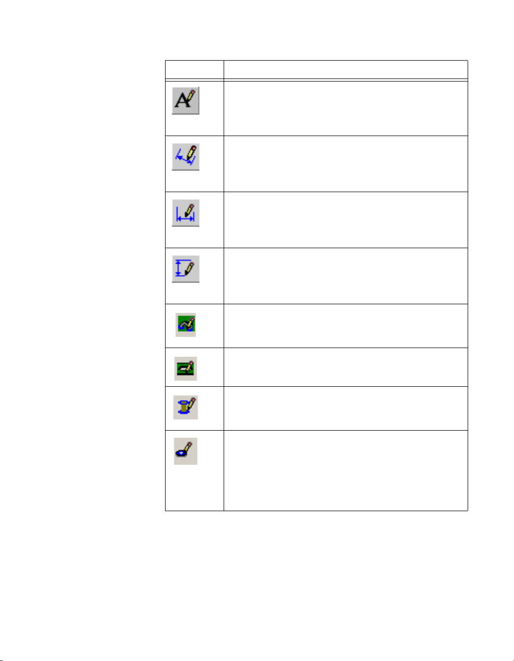
Place Toolbar
Chapter 1 User Interface
Button Description
Space Down Plus button. Increases vertical space
between two or more objects.
Space Down Min button. Decreases vertical space
between two or more objects.
The Place toolbar contains the functions used to place elements such as
traces, lines and polygons on the design. The Place toolbar buttons are
explained in the table below.
Button Description
Place Comment button. Places a comment on the design.
Refer to the Placing a Comment section of Chapter 8,
Preparing for Manufacturing/Assembly, for more
information.
Capture Area button. Captures a section of the screen
and places it on the system clipboard.
Select button. De-activates any selected mode (for
example, for placing traces) and allows you to select an
element on the board.
Place Line button. Places a line on the design (or place a
trace, when used on a copper layer). Refer to the Placing
Shapes and Graphics section of Chapter 4, Working with
Parts, for more information.
Place Arc button. Places an arc on the design. Refer to the
Placing Shapes and Graphics of Chapter 4, Working with
Parts, section for more information.
Place Bezier button. Places a bezier curve on the design.
Refer to the Placing Shapes and Graphics section of
Chapter 4, Working with Parts, for more information.
Place Circle button. Places a circle on the design. Refer
to the Placing Shapes and Graphics section of Chapter 4,
Working with Parts, for more information.
© National Instruments Corporation 1-9 NI Ultiboard User Manual
Page 26
Chapter 1 User Interface
Button Description
Place Ellipse button. Places an ellipse on the design.
Refer to the Placing Shapes and Graphics section of
Chapter 4, Working with Parts, for more information.
Place Pie button. Places a pie-shape on the design. Refer
to the Placing Shapes and Graphics section of Chapter 4,
Working with Parts, for more information.
Place Rounded Rectangle button. Places a rectangle
with rounded corners. Refer to the Placing Shapes and
Graphics section of Chapter 4, Working with Parts, for
more information.
Place Rectangle button. Places a rectangle on the design.
Refer to the Placing Shapes and Graphics section of
Chapter 4, Working with Parts, for more information.
Place Polygon button. Places a polygon on the design.
Refer to the Placing Shapes and Graphics section of
Chapter 4, Working with Parts, for more information.
Place Copper Area button. Places a polygon copper area
on the design. Refer to the Placing Copper Areas section
of Chapter 5, Working with Traces and Copper, for more
information.
Follow-me button. Places a follow me trace, a trace that
automatically draws a legal trace between two selected
points. Refer to the Placing a Trace: Follow-me Method
section of Chapter 5, Working with Traces and Copper,
for more information.
Place Multiple Traces as a Bus button. Use to connect
multiple traces between multi-pinned devices such as ICs.
Refer to the Placing a Bus section of Chapter 5, Working
with Traces and Copper, for more information.
Place Group Array Box button. A group array box is
used to place parts in an array. Refer to the Placing a
Group Array Box section of Chapter 4, Working with
Parts, for more information.
NI Ultiboard User Manual 1-10 ni.com
Page 27
Button Description
Place Text button. Places text on the design. Useful for
annotation purposes. Refer to the Placing and Editing
Text section of Chapter 8, Preparing for
Manufacturing/Assembly, for more information.
Place a Standard Dimension button. Places a dimension
between any two selected points. Refer to the Working
with Dimensions section of Chapter 4, Working with
Parts, for more information.
Place a Horizontal Dimension button. Places a
horizontally-oriented dimension between two selected
points. Refer to the Working with Dimensions section of
Chapter 4, Working with Parts, for more information.
Place a Vertical Dimension button. Places a
vertically-oriented dimension between two selected
points. Refer to the Working with Dimensions section of
Chapter 4, Working with Parts, for more information.
Place a Net Bridge button. Places a net bridge
connection. Refer to the Net Bridges section of Chapter 5,
Working with Traces and Copper, for more information.
Chapter 1 User Interface
Place a Hole button. Places a hole on your PCB.
Place a Via button. Places a via on the design. Refer to
the Working with Vias section of Chapter 5, Working with
Traces and Copper, for information.
Place Pins button. Places pins on the design when editing
or creating a part in In-place Edit mode or Footprint Edit
mode. Refer to the Editing a Placed Part (In-Place Edit)
and Using the Database Manager to Create a Part
sections of Chapter 4, Working with Parts, for more
information.
© National Instruments Corporation 1-11 NI Ultiboard User Manual
Page 28
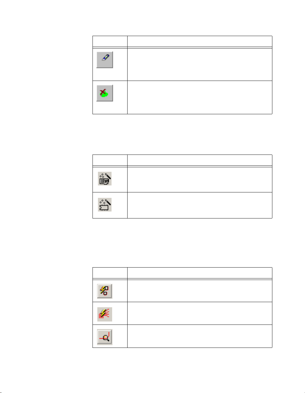
Chapter 1 User Interface
Wizard Toolbar
Button Description
Polygon Splitter button. Splits copper areas and
powerplanes. Refer to the Splitting Copper section of
Chapter 5, Working with Traces and Copper, for more
information.
Remove Copper Islands button. Removes copper
islands. Refer to the Placing Copper Areas section of
Chapter 5, Working with Traces and Copper, for more
information.
The Wizard toolbar contains the wizard functions supported by Ultiboard.
The Wizard toolbar buttons are explained in the table below.
Button Description
Board Wizard button. Starts the Board Wizard. Refer to
the Working with the Board Outline section of Chapter 3,
Setting Up a Design, for more information.
Part Wizard button. Starts the Part Wizard. Refer to the
Using the Part Wizard to Create a Part section of
Chapter 4, Working with Parts, for more information.
Autoroute Toolbar
The Autoroute toolbar contains the autorouting and placement functions
supported by Ultiboard. The Autoroute
table below.
Button Description
Begin Autoplacing button. Starts automatically placing
parts.
Autoroute Selected Buses button. Displays the Bus
Autorouting dialog.
Start Trace Optimization button. Starts trace
optimization.
NI Ultiboard User Manual 1-12 ni.com
toolbar buttons are explained in the
Page 29
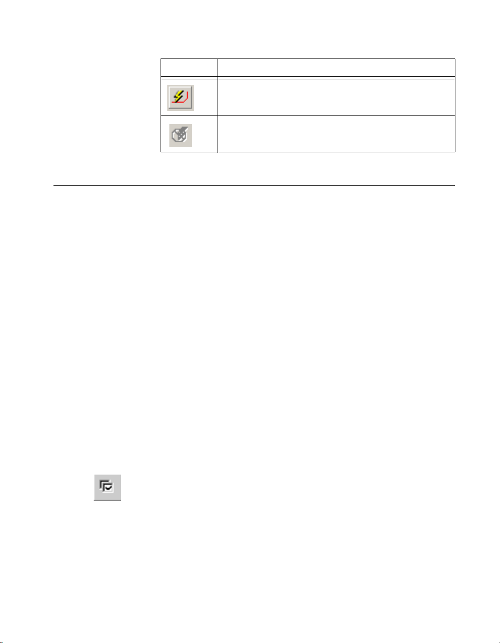
Button Description
Setting Preferences
This section explains general procedures for setting preferences. The
following sections describe details of setting specific options.
Complete the following steps to set your user preferences:
1. Choose Options»Global Preferences. The Preferences dialog box
appears, offering you the following tabs:
• General Tab
• Paths Tab
• Colors Tab
• PCB Design Tab
• Dimensions Tab
• 3D Options Tab
2. Select the desired tab.
3. Set the desired customization options. The specific options and
settings available in the tabs are described in the following sections.
4. Click OK to save your changes.
Chapter 1 User Interface
Start/Resume Autorouting button. Starts automatically
placing traces.
Stop/Pause Autorouter button.
General Tab
Complete the following steps to change workspace options:
1. Choose Options»Global Preferences and select the General tab.
2. Set the Fullscreen mode, View, Crosshair and Mouse wheel
behavior settings as desired.
3. Set the following as desired:
• Auto save settings—Enable to have changes automatically saved
(at the specified Time interval).
• Minimum control point size—The size of the contol points on
vertices and other objects.
© National Instruments Corporation 1-13 NI Ultiboard User Manual
Page 30

Chapter 1 User Interface
Paths Tab
• Line width cache size—The number of recently used line widths
Ultiboard keeps in memory. Minimum cache size is 5.
• Undo buffer size—The number of undo actions allowed.
• Load last file on startup—Enable if you would like to continue
working on the last file you had open in your previous Ultiboard
session.
• Unicode Settings box—If desired, enable the Save .TXT files as
plain text checkbox.
• Language—Select the desired language from the list. You must
restart Ultiboard for all dialog boxes to reflect the new setting.
4. To apply your changes but leave the Preferences
click Apply. To apply your changes and close the Preferences
box, click
OK.
dialog box open,
dialog
The Ultiboard installation puts specific files in specific locations. If
necessary you can point Ultiboard to a new location to find, for example,
database files. You can also use this dialog box to create and specify user
settings files that contain individuals’ preferences for all options.
Complete the following steps to change file locations:
1. Choose Options»Global Preferences. The Preferences dialog box
appears.
2. Select the Paths tab.
3. Change the following as desired:
• Circuit Default Path—This is where all new files are saved,
unless you manually navigate to a new location when saving.
• User Button Images Path—This is where you store any
user-created button graphics.
4. Change the User Settings as desired:
• Configuration File—Contains the user interface settings.
• New User Configuration File—Click to create a new user
configuration file and select an item from the drop-down list.
5. Change the settings in the Database Files area as desired:
• Master Database—The location of the Master Database.
• Corporate Database—The location of the Corporate Database.
• User Database—The location of the User Database.
NI Ultiboard User Manual 1-14 ni.com
Page 31

Colors Tab
Chapter 1 User Interface
Ultiboard allows you to set up color schemes for the workspace
background and other displayed elements.
Complete the following steps to set up color schemes:
1. Choose Options»Global Preferences. The Preferences dialog box
appears.
2. Select the Colors tab and complete the following as required:
• To apply an existing color scheme, either the default or one you
have created, choose from the Color scheme drop-down list.
• To modify an existing color scheme, choose it from the Color
scheme drop-down list. From the Color element drop-down list,
choose the element whose color you want to modify. Click the
color button (unlabelled) and choose a new color for that element.
Your change is stored with the color scheme when you click
Apply or OK.
• To create a color scheme, click New scheme and provide a scheme
name. The element colors remain at the value they had in the most
recently loaded scheme. Modify the element colors as described
above, and save your changes by clicking Apply or OK.
• To add a color element, click New element and enter a name. The
element appears in the Color element list, and you can choose a
color for the element.
• Optionally, enable the Preview grayed out checkbox to switch
the preview visibility on or off and adjust and select the Grayed
out factor.
Your changes are reflected in the Preview area.
3. To apply your changes but leave the Preferences
click Apply. To apply your changes and close the Preferences
box, click
OK.
dialog box open,
dialog
PCB Design Tab
Use the PCB Design tab of the Preferences dialog box to define a variety
of actions associated with the overall PCB design.
Complete the following steps to define the default actions:
1. Choose Options»Global Preferences. The Preferences
appears.
2. Select the PCB Design tab.
© National Instruments Corporation 1-15 NI Ultiboard User Manual
dialog box
Page 32

Chapter 1 User Interface
3. Set the viewing options in the View area:
• Show pin 1 mark—Enable to display pin 1 of a device with a
unique marking.
• Show Copper Areas—Enable to display copper areas. This
applies to copper areas only, not regular polygon shapes on
non-copper layers.
• Show pin info in pin—Enable to display the pin number and hole
size when zoomed in.
4. In the On select entire trace area:
• Select Across Layers—Enable so that when you choose
Edit»Select Entire Trace, the trace will be selected across all
layers, instead of just the active layer.
5. In the Part Drag area:
• Re-route after move—Enable if you would like the traces that
are attached to a part to be re-routed if you move the part.
6. In the Default pin diameters area:
• Units—Select unit of measurement from drop-down list.
• Jumpers—Enter the default pin diameter for jumpers.
• Testpoints—Enter the default pin diameter for testpoints.
7. In the Action on DRC error area, set the actions to be taken when
Ultiboard encounters a Design Rule Error:
• Cancel the current action—Enable to prevent the current
operation from being completed. For example, placing a trace
over a pad that is part of a different netlist will not be permitted.
• Ask for Confirmation—Enable so that if an invalid operation is
attempted a prompt is given asking if the operation should be
completed even though a Design Rule will be violated.
• Overrule—Enable to permit the operation to be completed.
8. In the On trace deletion area:
• Auto delete Via (standard)—Enable to have vias automatically
deleted when you delete the trace associated with that via.
• Auto delete teardrop—Enable to have teardrops automatically
deleted when you delete the trace associated with that teardrop.
NI Ultiboard User Manual 1-16 ni.com
Page 33

Chapter 1 User Interface
9. In the On trace placement area:
• Auto trace narrowing—Enable to allow traces to narrow as
necessary during routing.
• Auto add teardrop—Enable to add a teardrop when a trace is
placed.
10. In the DRC & Net check area:
• No Realtime Check—Enable to prevent a DRC and netcheck in
“real time” as you place objects, for example, parts.
• Check on action end—Enable to perform a DRC and netcheck
after each action, for example, part placement.
• Full Realtime Check—Enable to perform DRC checks and
ratnest updates to your work in “real time” (as you place objects,
for example, parts).
11. In the Follow me router area:
• Continuous place—Enable to have the next trace begin from the
finish point of the previous trace when placing a “Follow-me”
trace. If this is not selected, you must click to start a new trace.
Refer to the Placing a Trace: Follow-me Method section in Chapter 5,
Working with Traces and Copper, for information about Follow-me
traces.
12. In the Crosshair area:
• Trace snap—Enable to have the pointer snap to the nearest trace.
Refer to the Working with Traces section in Chapter 5, Working with
Traces and Copper, for information about using trace snap.
13. In the Post processing area:
• Show fiducial marks—Enable to show fiducial marks when you
postprocess this design. Fiducial marks are used to align layers
with each other. As shown in the figure below, Ultiboard uses
three different types of cocentric circles as fiducial marks. These
are placed on three of the four corners of a design when it is
printed or exported to Gerber.
© National Instruments Corporation 1-17 NI Ultiboard User Manual
Page 34

Chapter 1 User Interface
Dimensions Tab
14. To apply your changes but leave the Preferences dialog box open,
click Apply. To apply your changes and close the Preferences
dialog
box, click OK.
Use the Dimensions tab of the Preferences dialog box to define the
characteristics to be used for any dimensions placed in the board. Refer to
the Working with Dimensions section of Chapter 4, Working with Parts, for
information about placing dimensions.
Complete the following steps to define the default dimension
characteristics:
1. Choose Options»Global Preferences. The Preferences
dialog box
appears.
2. Click the Dimensions tab.
3. Set the following as desired:
• Units—This is the unit of measure for Stub Length, Arrow Style
and Text Style.
• Stub Length—This is the amount the end lines of the dimension
protrude above eacg arrowhead.
• Arrow Style—This is where you adjust the size and appearance
of the arrow.
• Text Style—This is where you adjust the size and appearance of
the text.
NI Ultiboard User Manual 1-18 ni.com
Page 35

3D Options Tab
Chapter 1 User Interface
• Displayed Unit—Select the unit of measure to be displayed with
the dimension. If you select Use Design Settings, the unit of
measure selected in the Design Units field of the Grids & Units
tab of the PCB Properties dialog box are used. This setting also
appears in the Draw Settings toolbar.
• Alignment and Position—These are where you set how the text
appears in relation to the arrow.
• Orientation—This is where you select the angle at which the
dimension displays.
The results of your choices are previewed on the tab.
4. To apply your changes without closing the dialog box, click Apply.
Existing dimensions are not affected. To apply your changes and close
the dialog box, click OK.
Complete the following steps to set 3D viewer options:
1. Choose Options»Global Preferences
and select the 3D Options tab.
2. To change the background color in the 3D viewer, click on the shaded
rectangle beside Background color. The Color dialog box appears.
3. Select the desired color and click OK in the Color dialog box.
4. Optionally, enable the Show Copper and Silkscreen while moving
checkbox.
5. Set the Internal View Options as desired.
Tip The more space that you set between the layers, the easier they will be to view when
you zoom in on the PCB in the 3D mode. Refer to the Internal View section of Chapter 9,
Viewing Designs in 3D, for more information.
6. To apply your changes but leave the Preferences
click Apply. To apply your changes and close the Preferences
dialog box open,
dialog
box, click OK.
© National Instruments Corporation 1-19 NI Ultiboard User Manual
Page 36

Chapter 1 User Interface
Setting PCB Properties
Many characteristics of your PCB design are controlled through the PCB
Properties dialog box including the number of layers, design rules and grid
settings. These settings are saved with the design and will be in effect when
the design is reopened.
Do one of the following to display the PCB Properties dialog box for the
board:
• With nothing selected on the board, right-click on an empty portion of
the board and choose Properties from the context menu that appears.
• Click on an empty portion of the board and choose Edit»Properties.
• Double-click on an empty portion of the board.
Attributes Tab
All properties dialog boxes for all design elements have an Attributes tab,
although a design’s PCB typically does not have any attributes. Refer to the
Attributes section of Chapter 4, Working with Parts, for information about
adding attributes.
Grid & Units Tab
Use the Grid & Units tab of the PCB Properties dialog box to control
Ultiboard grids and set the unit of measurement for your design.
Complete the following steps to set up the grid properties:
1. Choose the default units of measure from the Design Units list.
2. In the Grid area, set the following elements as desired:
• Grid Type—Select Standard Grid for a rectangular grid, or
Polar Grid, for a circular grid.
• Visible grid style—This is where you set the style for the Visible
Grid. (The Visible Grid provides a visual reference for you to
visually align parts and traces).
• Visible grid—This is the distance between the grid’s elements
(dots, lines or crosses) that you set up in the Visible grid style
field.
• Grid Step Name—Use this field to change the distance between
a grid’s elements. Select the desired grid: Part Grid; Copper
Grid; Via Grid; SMD Grid, and then enter the desired increment
in the Grid Step Value field.
NI Ultiboard User Manual 1-20 ni.com
Page 37
Copper Layers Tab
Chapter 1 User Interface
• Degree Step—This field becomes active when Polar Grid is
selected in the Grid Type field. Enter the desired distance
between the grid’s elements (dots, lines or crosses). Select the unit
of measure in the drop-down list to the right of this field—choices
are: degrees, radians, or grads.
• Grid start offset—This field becomes active when Polar Grid is
selected in the Grid Type field. Enter the distance to offset the
center of the polar grid: X is horizonatal offset; Y is vertical offset.
3. Click OK to close the dialog.
To show or hide the visible grid, select View»Grid.
Use the Copper Layers tab of the PCB Properties dialog box to determine
the layer pairs that are acceptable for blind, buried or micro vias. This is
used when you try to place a via. Your choices will affect the cost of the
board, and should be confirmed with the board manufacturer.
This tab also allows you to set the default clearance for the board—the
distance from the edge of the board that is to be kept free of any other
elements. For example, if you try to run a trace through a clearance, or try
to place a part so that a pad is put within a clearance, a design rule error
occurs.
Note If you used the Board Wizard, the layer information and clearance may already
have been set. Refer to the Using the Board Wizard section of Chapter 3, Setting Up a
Design, for more information.
Complete the following steps to set up the Copper Layers tab:
1. Set the number of layer pairs you intend to use by entering the value or
using the up/down arrows in the Layer Pairs field. There should be at
least one layered pair to act as a core.
2. Set the number of Single Layer Build-ups for both the top and
bottom. There should be at least one layered pair to act as a core.
3. Select the Micro Vias, Buried Vias, or Blind Vias checkboxes to use
these in your design.
© National Instruments Corporation 1-21 NI Ultiboard User Manual
Page 38

Chapter 1 User Interface
4. As you make changes to the layer settings, the Allowed Vias pane
shows the acceptable layer combinations for blind and buried vias or
microvias. Use the checkboxes to select the layer combinations you
want to allow in your design as shown in the example in the figure
below.
5. In the Allow Routing area, from the Copper Layer drop-down list,
select the copper layer for which you wish to assign routing properties
and click Properties to display the Copper Layer Properties dialog
box.
Enable the Routable checkbox to allow routing on the selected layer.
In the Trace Bias drop-down list, select one of Horizontal; Vertical;
or None.
Click OK to close the Copper Layer Properties dialog box.
6. In the Board area, enter the desired Board Outline Clearance and
Board Thickness.
7. Click OK to close the dialog box.
Pads/Vias Tab
Use the Pads/Vias tab of the PCB Properties dialog box to set the
following:
• Through Hole Pad Annular Ring
• Vias
• Microvias
• Maximum Vias Per Net
• Surface Mount Pads Oversize
NI Ultiboard User Manual 1-22 ni.com
Page 39

Chapter 1 User Interface
Through Hole Pad Annular Ring
Footprints in the database have been designed with pad sizes in accordance
with the manufacturers’ recommendations. To change these settings you
can edit the footprint in the database or directly on the design using the
In-place Part Edit command. Alternatively, you can apply a set of design
rules to specific footprints or to the entire design.
The annular ring setting (the ring of copper around the drill hole of a pad or
via) allows you to specify either a fixed value (for example, 50 mils) or a
relative value that depends on the radius of the drill hole size. For example,
a 50 mil drill hole (radius of 25 mils) with a relative value of .6 (60%) will
create an annular ring of 15 mils (60% of 25 mils). When using relative
settings, it is important to choose minimum and maximum values to ensure
that the annular ring will never go beyond those bounds.
Complete the following to enter an annular ring setting:
1. Click the button beside the desired field (Top, Inner or Bottom) in the
Pad/Vias tab. The Through Hole Pad Properties dialog box appears.
Choose Fixed and enter the fixed value.
Or
Choose Relative and enter the relative setting. Be sure to choose Min
and Max values.
Complete the following to apply the design rules to a footprint:
1. Select the footprint and choose Edit»In-Place Part Edit.
2. Select the pads to which the rule should apply.
3. Right-click and, from the context menu, choose Properties.
4. On the
Pad tab of the properties dialog box, enable Use Design Rules.
Vias
The Vias setting sets the default Drill Diameter and Pad Diameter to be
used when a via is placed during trace placement. This setting also applies
to vias that have already been placed in the design.
Microvias
The Micro Vias area is where you set the default via dimensions to be used
when a microvia is placed during trace placement. This setting will also
apply to microvias that have already been placed in the design.
© National Instruments Corporation 1-23 NI Ultiboard User Manual
Page 40

Chapter 1 User Interface
General Layers Tab
The Capture Land Diameter field determines the land diameter where the
microvia starts, while Target Land Diameter determines the diameter
where the microvia ends. These terms are in accordance with the IPC and
JPCA joint standard IPC/JPCA-2315, Design Guide for High Density
Interconnects (HDI) and Microvias. The Maximum Layer Span is either
one or two layers.
Maximum Vias Per Net
The Nets area is where you set up the maximum number of vias allowed
per net.
Surface Mount Pads Oversize
Depending on the manufacturing process you are using, you may wish to
enlarge the size of all surface mount pads by a fixed amount. This can be
set independently for the Top and Bottom layers. The setting refers to the
amount that will be added to the pad. In the case of a circular pad this
amount is added to the radius. In the case of a rectangular or square pad the
amount will be added to the width and length.
Use the General Layers tab of the PCB Properties dialog box to control
which layers are available on the board.
Complete the following steps to control the numbers of layers in the board:
1. Add layers to the board by selecting the checkbox beside the layer
name.
2. Remove layers from the board by clearing the checkbox beside the
layer name.
Note You can have a layer available on the board, and temporarily dim or hide it. Refer to
the Accessing Layers section of Chapter 3, Setting Up a Design, for more information.
Note There are up to ten mechanical CAD layers in PCB design. These layers allow you
to provide information that is directly related to the PCB. You place elements on them to
represent the mechanical elements of your design – for example, cabinet casing or
mounting brackets.
NI Ultiboard User Manual 1-24 ni.com
Page 41

Design Rules Tab
Chapter 1 User Interface
Complete the following steps to rename layers:
1. Click Rename in the Layer Names area. The Select Layer for
Renaming dialog box appears.
2. Select the layer that you wish to rename and click OK. The Layer
dialog box appears.
3. Enter the new Layer Name and click OK.
Complete the following steps to set the design rules for the PCB:
1. Click on the Design Rules tab.
2. In the Design Rule Default Values area, set the following as desired:
• Trace Width Settings—Set trace width and minimum and
maximum trace width.
• Trace Length Settings—Set minimum and maximum trace
length.
• Trace Neck Settings—Set minimum and maximum trace neck
length.
• Clearance Settings—Set clearance to traces, pads, vias and
copper areas. For all of these clearances to be active, and display
in the Spreadsheet View, the Use multiple clearances checkbox
must be selected. Otherwise, only clearance to traces will be
operational.
• Part Spacing Settings—Set minimum distance between parts.
This setting only applies to the spacing during part shoving.
Tip To set this option for an individual part, go to the Part tab of that part’s properties
dialog box. Refer to the Shoving Parts section of Chapter 4, Working with Parts, for more
information.
• Pin & Gate Swapping Settings—Set parameters for pin and gate
swapping.
• Thermal Relief—Set the thermal relief shape.
• Drill Technology—Set the minimum tool size for slot drilling.
For information on any setting, select it in the Design Rule Default Values
area. A description appears in the field at the bottom of the dialog.
© National Instruments Corporation 1-25 NI Ultiboard User Manual
Page 42

Chapter 1 User Interface
Setting Favorite Layers
You can assign shortcuts for up to ten layers using the Favorite layers tab.
These shortcuts can then be used to make a layer active. The active layer is
the layer where any new elements will be placed, or where any deletions
will be made.
Complete the following steps to assign shortcut numbers to layers:
1. Click on the Favorite layers tab.
2. Select the desired layer from the drop-down list beside each layer
number. For example, you may wish to assign Layer 2 to the
Copper Bottom layer.
3. Click OK.
To make a layer active, press <Ctrl-Alt-layer number> on your keyboard.
The layer becomes active and is highlighted in the Layers tab of the Design
Toolbox.
In the above example, pressing <Ctrl-Alt-2> on your keyboard makes the
Copper Bottom layer active.
NI Ultiboard User Manual 1-26 ni.com
Page 43

Design Toolbox
The Design Toolbox, shown in the figure below, is a vital part of the user
interface. You will use it often to manage your design efforts by controlling
major parts of Ultiboard’s functionality. To toggle it on or off, select
View»Design Toolbox.
Chapter 1 User Interface
The Design Toolbox is made up of two tabs:
• The Projects tab lets you view the projects that are currently open.
Each project may contain one or more designs. Double-click to make
a particular design the current view.
• The Layers tab lets you move between layers of your design, control
the appearance of layers, and perform several other functions.
© National Instruments Corporation 1-27 NI Ultiboard User Manual
Page 44
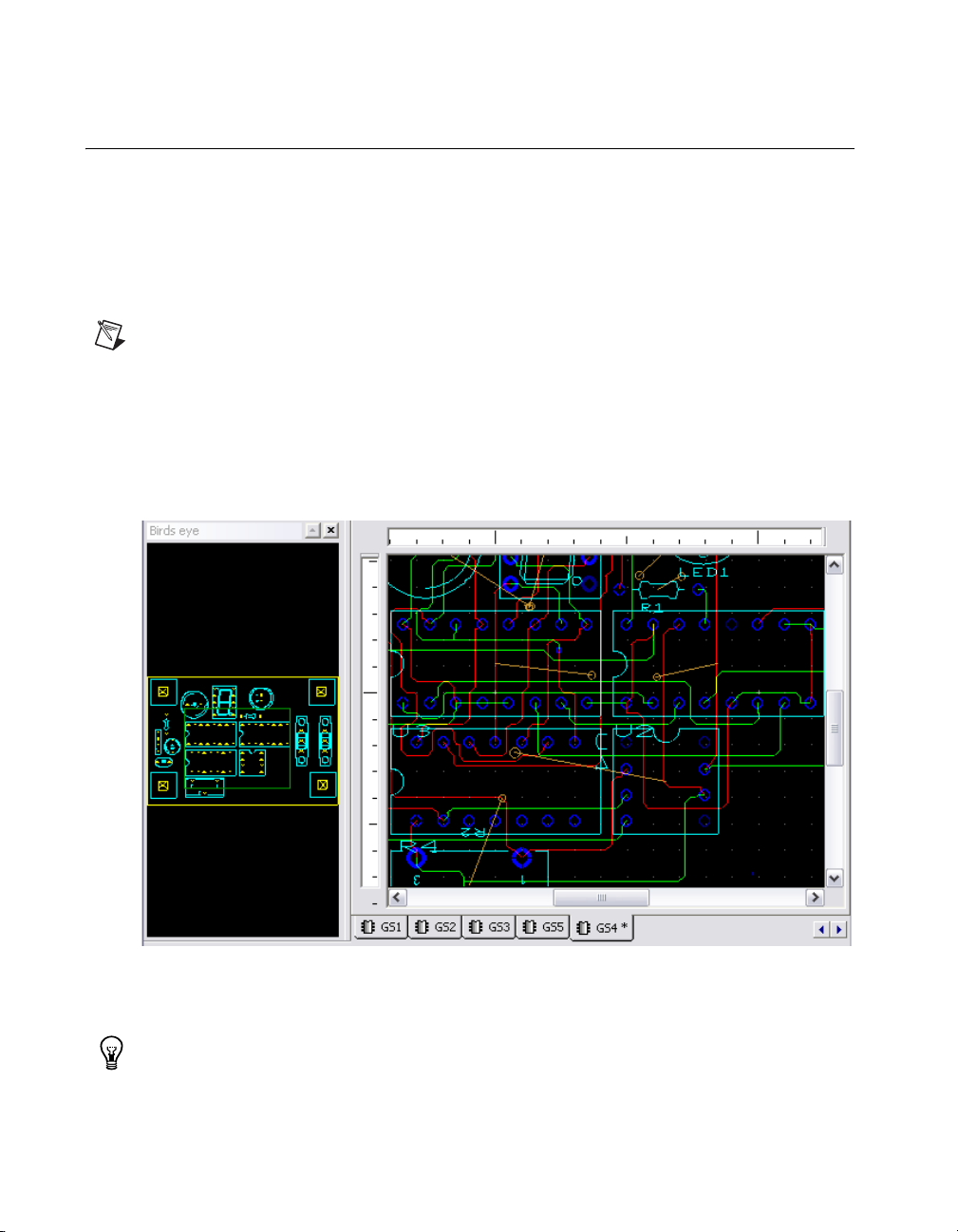
Chapter 1 User Interface
Birds Eye View
Note All layers appear in the Birds Eye View, whether or not they have been disabled in
the Layers tab of the Design Toolbox.
The Birds Eye View shows you the design at a glance and lets you easily
navigate around the workspace.
To magnify a specific area on the design, drag a rectangle around the
desired area on the Birds Eye View. The rectangle snaps to the same ratio
as the design space.
In the example in the figure below, the green rectangle that was drawn
encloses the four ICs in the middle of the Birds Eye View, and the design
has magnified to display only the items that are selected within this
rectangle.
To move the rectangle, hold down the right mouse button anywhere over the
Birds Eye View, and drag the rectangle to the desired location.
Tip You cannot resize the selection rectangle in the Birds Eye View. Instead, you must
draw another rectangle of the required size. When you do this, the original rectangle
disappears.
NI Ultiboard User Manual 1-28 ni.com
Page 45
Spreadsheet View
The Spreadsheet View allows fast advanced viewing and editing of
parameters including part details such as footprints, Reference Designators,
attributes and design constraints.
By default, the Spreadsheet View does not appear until you have
opened a project. To toggle the Spreadsheet View on and off, select
View»Spreadsheet View.
The following buttons are available in the Spreadsheet View.
Note The buttons do not appear in all tabs.
Button Description
Chapter 1 User Interface
Export to Textfile button. Displays a standard Windows
Save dialog where you save the selection as a textfile.
Export to CSV File button. Displays a standard
Windows Save dialog where you save the selection as a
file with comma-separated values.
Export to Excel button. Click to open a Microsoft® Excel
spreadsheet with the selected data displayed. (You must
have Excel installed to use this function).
Sort Ascending button. Sorts the selected column in
ascending order.
Sort Descending button. Sorts the selected column in
descending order.
Print button. Prints the data in the selected tab.
Select All button. Selects all elements in the tab.
Copy button. Copies the selection to the clipboard.
© National Instruments Corporation 1-29 NI Ultiboard User Manual
Page 46

Chapter 1 User Interface
Note You can also access the above commands from a pop-up menu by right-clicking in
the Spreadsheet View.
Button Description
Find and Select the Part button. Zooms in on the
selected part. Refer to the Using the Parts Tab for Other
Functions section of Chapter 4, Working with Parts, for
more information.
Lock the Selected Part button. Locks the selected
unlocked parts or unlocks the selected locked parts. Refer
to the Using the Parts Tab for Other Functions section of
Chapter 4, Working with Parts, for more information.
Start Placing the Unpositioned Parts button. Refer to
the Using the Parts Tab to Place Parts section of
Chapter 4, Working with Parts, for more information.
Show preview button. Toggles the Spreadsheet View’s
Preview function on and off. Refer to the Using the Parts
Tab for Other Functions section of Chapter 4, Working
with Parts, for more information.
Spreadsheet View: DRC Tab
The DRC tab displays errors (for example, Design Rule Errors) and
warnings as they occur while you work. Errors are labeled with red
triangles, and warnings are labeled with yellow circles, as shown in the
example in the figure below.
Double-click on an error or warning to go to its location on the workspace.
NI Ultiboard User Manual 1-30 ni.com
Page 47

Chapter 1 User Interface
When you right-click on an item in the DRC tab, a pop-up menu displays
with the following available selections:
• Copy—Copies all items in the
DRC tab and places them on the
clipboard.
• Go to Error/Tag—Click to go to the highlighted error or warning on
the workspace.
• Add to Filter—Click to filter out the selected error/warning type. This
type of error/warning will no longer show in the DRC tab.
• Remove all filters—Click to remove all error/warning types from the
filter. All errors and warnings will now show in the DRC tab.
• Start Filter Manager—Click to start the Filter Manager. Refer to the
Filter Manager section for more information.
Filter Manager
Use the Filter Manager to filter desired errors & warnings out of the DRC
tab in the Spreadsheet View.
Complete the following steps to use the Filter Manager:
1. Right-click in the DRC tab of the Spreadsheet View and select Start
filter manager from the pop-up that appears.
The Filter Manager dialog box appears with a list of errors and
warnings that are filtered out of the DRC tab. If this is the first time
you are accessing this dialog box, it will be empty.
2. Click Add Filter to display the Add Filter(s) dialog box.
© National Instruments Corporation 1-31 NI Ultiboard User Manual
Page 48

Chapter 1 User Interface
3. Select the error type(s) to add to the filter. You can use the Ctrl and
Shift keys to select multiple items.
4. Click OK to close the Add Filter(s) dialog box and add the selected
items to the Filter Manager.
5. Click Close to close the Filter Manager dialog box. The selected error
types no longer display in the DRC tab.
To remove an error type from the Filter Manager, select the error type and
click Remove Filter.
To remove all error types, click Remove All.
Spreadsheet View: Results Tab
The Results tab displays the results of searching for elements in the design.
Refer to the Searching for Design Elements section of Chapter 2,
Beginning a Design, for more information.
It also displays the results of running a connectivity check. Refer to the
Design»Connectivity Check section of Appendix A, Menus and
Commands, for more information.
Note The Results tab flashes red when it contains new data.
Double-click a line in this tab to zoom in on the corresponding area of the
design.
NI Ultiboard User Manual 1-32 ni.com
Page 49

You can also right-click an item to display a popup that contains Copy;
Clear Results; Go to.
Spreadsheet View: Parts Tab
Use the Parts tab to work with the parts in your design. Refer to the Using
the Parts Tab in the Spreadsheet View section of Chapter 4, Working with
Parts, for more information.
Column Description
(unlabelled) The colored circle indicates whether the part has been
Chapter 1 User Interface
placed on the board outline (bright green), or is off to
the side awaiting placement (dark green). Orange
indicates the part has been locked.
RefDes The part’s Reference Designator (unique identifier).
Value The part’s value, for example, 150 pF for a capacitor.
Shape The physical footprint of the part.
Locked Yes indicates that the part cannot be moved. No
indicates that the part can be moved.
Trace
Clearance
Part Spacing This is the minimum spacing allowed between parts.
© National Instruments Corporation 1-33 NI Ultiboard User Manual
This is the minimum spacing allowed between the
part and any trace. You can enter a value here, or use
the Group Editor. Refer to the Working with the
Group Editor section of Chapter 3, Setting Up a
Design, for more information.
You can enter a value here, or use the Group Editor.
Refer to the Working with the Group Editor section of
Chapter 3, Setting Up a Design, for more information.
Page 50

Chapter 1 User Interface
Column Description
Pin Swap If enabled, allows like-pins to be swapped during the
routing process. You can choose either No (not
enabled), Yes or Use Group Settings. Refer to the
Working with the Group Editor section of Chapter 3,
Setting Up a Design, for more information.
Gate Swap If enabled, allows like-gates, to be swapped during the
routing process. You can choose Internal Gates
Only, which will swap gates within the same IC; No
Swapping; Advanced Swapping, which will swap
gates between ICs (both devices must be set to
Advanced Swapping); or Use Group Settings. Refer
to the Working with the Group Editor section of
Chapter 3, Setting Up a Design, for more information.
Part Group The group in which the part is placed. You can select
No Group or an existing group from the drop-down
list. Parts groups are created in the Group Editor.
Refer to the Working with the Group Editor section of
Chapter 3, Setting Up a Design, for more information.
Spreadsheet View: Part Groups Tab
Use the Part Groups tab to work with part groups as described in the table
below.
Column Description
Part Group This is the group in which the part is contained. Refer
to the Working with the Group Editor section of
Chapter 3, Setting Up a Design, for more information.
Trace
Clearance
Part Spacing This is the minimum spacing allowed between parts in
NI Ultiboard User Manual 1-34 ni.com
This is the minimum spacing allowed between the
parts in the group and any trace. You can enter a value
here, or use the Group Editor. Refer to the Working
with the Group Editor of Chapter 3, Setting Up a
Design, section for more information.
the group. You can enter a value here, or use the
Group Editor. Refer to the Working with the Group
Editor of Chapter 3, Setting Up a Design, section for
more information.
Page 51

Column Description
Pin Swap If enabled, allows pins for like-parts to be swapped
Gate Swap If enabled, allows like-gates, to be swapped during the
Locked Yes indicates that the part cannot be moved. No
Spreadsheet View: Nets Tab
Use the Nets tab to work with the net lists in your design. Refer to the Using
the Nets Tab section for more information.
Column Description
(unlabelled) The colored circle indicates whether the copper for
Chapter 1 User Interface
during the routing process.
routing process. You can choose Internal Gates
Only, which will swap gates within the same IC; No
Swapping; or Advanced Swapping, which will swap
gates between ICs (both devices must be set to
Advanced Swapping).
indicates that the part can be moved.
the net has been routed, that is, placed on the board
outline (bright green), or is awaiting placement (dark
green). Orange indicates the copper for the net has
been locked. You cannot lock the net until it has been
routed.
Net Name The net’s unique identifier.
Locked Yes indicates that the net cannot be moved. No
indicates that the net can be moved. You cannot lock
a net until it has been routed.
Trace Width The “default” width of the trace that is placed during
routing. You can enter a value here, or use the Group
Editor. Refer to the Working with the Group Editor of
Chapter 3, Setting Up a Design, section for more
information.
Max Width The maximum width to which a trace will be laid
during routing. You can enter a value here, or use the
Group Editor. Refer to the Working with the Group
Editor of Chapter 3, Setting Up a Design, section for
more information.
© National Instruments Corporation 1-35 NI Ultiboard User Manual
Page 52

Chapter 1 User Interface
Column Description
Min Width The minimum width to which a trace will be laid
during routing. You can enter a value here, or use the
Group Editor. Refer to the Working with the Group
Editor of Chapter 3, Setting Up a Design, section for
more information.
Topology The topology of the net as set in the Netlist Editor.
Choices are Shortest, Daisy Chain and Star. Refer to
the Using the Netlist Editor section of Chapter 5,
Working with Traces and Copper, for more
information. This feature is not available in all
versions of Ultiboard.
Trace Length Length of the routed net.
Max Length Maximum allowable length of copper in a net. Not
applicable (N/A) if Topology is set to Shortest.
Min Length MInimum allowable length of copper in a net. Not
applicable (N/A) if Topology is set to Shortest.
Trace
Clearance
This is the minimum spacing allowed between the
parts in the group and any trace. You can enter a value
here, or use the Group Editor. Refer to the Working
with the Group Editor section of Chapter 3, Setting
Up a Design, for more information.
Routing
Layers
The routing layers assigned to this net group. Click to
display the Layers to Apply dialog box, where you
set the layers to use for routing copper.
Routing
Priority
The routing priority for the selected net. 1 is the
highest priority, 2 the second highest, etc. Leave as
None if priority routing is not required. This feature is
not available in all versions of Ultiboard.
Net Group This is the group in which the net is contained. You
can either enter the group name here, or use the
Group Editor. Refer to the Working with the Group
Editor section of Chapter 3, Setting Up a Design, for
more information.
NI Ultiboard User Manual 1-36 ni.com
Page 53

Chapter 1 User Interface
Column Description
Bus Group This is the bus group in which the net is contained.
You can either enter the group name here, or use the
Group Editor. Refer to the Working with the Group
Editor section of Chapter 3, Setting Up a Design, for
more information.
Differential
Pair
This is the differential pair to which the net belongs.
Refer to the Working with the Group Editor section of
Chapter 3, Setting Up a Design, for more information.
Shield Net Use the drop-down list to select the net to use to shield
this net. This feature is not available in all versions of
Ultiboard.
Shield Width Width of the net’s shield. This feature is not available
in all versions of Ultiboard.
Show
Ratsnest
This is where you can show or hide the ratsnest for the
selected net. Refer to the Working with Ratsnests
section of Chapter 4, Working with Parts, for more
information.
Max Via
Count
This is the maximum number of vias allowed for the
selected net. You can use either the global settings, or
the group settings.
Via Drill
This is the diameter of the via pad’s hole.
Diameter
Via Pad
This is the diameter of the total via pad.
Diameter
© National Instruments Corporation 1-37 NI Ultiboard User Manual
Page 54

Chapter 1 User Interface
Spreadsheet View: Nets Groups Tab
Use the Net Groups tab to work with net groups.
Column Description
Net Group This is the group in which the net is contained. You
can either enter the group name here, or use the Group
Editor. Refer to the Working with the Group Editor
section of Chapter 3, Setting Up a Design, for more
information.
Trace Width The “default” width of the traces in the group that are
placed during routing. You can enter a value here, or
use the Group Editor. Refer to the Working with the
Group Editor of Chapter 3, Setting Up a Design,
section for more information.
Max Width The maximum width to which a trace in the group will
be laid during routing. You can enter a value here, or
use the Group Editor. Refer to the Working with the
Group Editor of Chapter 3, Setting Up a Design,
section for more information.
Min Width The minimum width to which a trace in the group will
be laid during routing. You can enter a value here, or
use the Group Editor. Refer to the Working with the
Group Editor section of Chapter 3, Setting Up a
Design, for more information.
Max Length Maximum allowable length of copper in a net group.
Not applicable (N/A) if Topology is set to Shortest.
Min Length MInimum allowable length of copper in a net group.
Not applicable (N/A) if Topology is set to Shortest .
Trace
Clearance
Routing
Layers
NI Ultiboard User Manual 1-38 ni.com
This is the minimum spacing allowed between the
traces in the group and any other trace. You can enter
a value here, or use the Group Editor. Refer to the
Working with the Group Editor of Chapter 3, Setting
Up a Design, section for more information.
The routing layers assigned to this net group. Click to
display the Layers to Apply dialog box, where you
set the layers to use for routing copper.
Page 55

Column Description
Chapter 1 User Interface
Routing
Priority
Locked Yes indicates that the part cannot be moved. No
Max Via
Count
The routing priority for the selected net group. 1 is the
highest priority, 2 the second highest, etc. Leave as
None if priority routing is not required. This feature is
not available in all versions of Ultiboard.
indicates that the part can be moved.
This is the maximum number of vias allowed in the
net group.
Spreadsheet View: SMT Pads Tab
Use the SMT Pads tab to work with pad information for surface-mount
devices.
Column Description
Pad Name The unique identifier for the pad, by RefDes and Pin
Number. For example, U1, P1 is pin number one of
the device with RefDes U1.
Pad Shape The shape of the pad as set in the SMT Pin
Properties dialog box. Refer to the Viewing and
Editing SMT Pin Properties section of Chapter 4,
Working with Parts, for more information.
Pad Radius The radius of the pad as set in the SMT Pin
Properties dialog box. Refer to the Viewing and
Editing SMT Pin Properties section of Chapter 4,
Working with Parts, for more information.
Pad Width The width of the pad as set in the SMT Pin
Properties dialog box. Refer to the Viewing and
Editing SMT Pin Properties section of Chapter 4,
Working with Parts, for more information.
Pad Height The height of the pad as set in the SMT Pin
Properties dialog box. Refer to the Viewing and
Editing SMT Pin Properties section of Chapter 4,
Working with Parts, for more information.
© National Instruments Corporation 1-39 NI Ultiboard User Manual
Page 56

Chapter 1 User Interface
Column Description
Trace
Clearance
Neck Length The default length of the neck where the trace attaches
Neck Max The maximum permitted length of the neck where the
Neck Min The minimum permitted length of the neck where the
The clearance of the trace to parts. You can use net
settings, or as set in the SMT Pin Properties dialog
box. Refer to the Viewing and Editing SMT Pin
Properties section of Chapter 4, Working with Parts,
for more information.
to the pin, as set in the SMT Pin Properties dialog
box. You can also enter the value here. Refer to the
Viewing and Editing SMT Pin Properties section of
Chapter 4, Working with Parts, for more information.
trace attaches to the pin, as set in the SMT Pin
Properties dialog box. You can also enter the value
here. Refer to the Viewing and Editing SMT Pin
Properties section of Chapter 4, Working with Parts,
for more information.
trace attaches to the pin, as set in the SMT Pin
Properties dialog box. You can also enter the value
here. Refer to the Viewing and Editing SMT Pin
Properties of Chapter 4, Working with Parts, section
for more information.
Min Width The minimum permitted trace width.
Spreadsheet View: THT Pads Tab
Use the THT Pads tab to work with pad information for through-hole
technology devices.
Column Description
Pad Name The unique identifier for the pad, by RefDes and Pin
Number. For example, U1, P1 is pin number one of
the part with RefDes U1.
Top Pad
Shape
NI Ultiboard User Manual 1-40 ni.com
The shape of the top layer pad as set in the Through
Hole Pin Properties dialog box. Refer to the Viewing
and Editing Through Hole Pin Properties section of
Chapter 4, Working with Parts, for more information.
Page 57

Column Description
Chapter 1 User Interface
Inner Pad
Shape
The shape of the inner layer pad as set in the Through
Hole Pin Properties dialog box. Refer to the Viewing
and Editing Through Hole Pin Properties section of
Chapter 4, Working with Parts, for more information.
Bottom Pad
Shape
The shape of the bottom layer pad as set in the
Through Hole Pin Properties dialog box. Refer to
the Viewing and Editing Through Hole Pin Properties
section of Chapter 4, Working with Parts, for more
information.
Annular Ring The size of the annular ring for this pad as set in the
Through Hole Pin Properties dialog box. Refer to
the Viewing and Editing Through Hole Pin Properties
section of Chapter 4, Working with Parts, for more
information.
Pad Diameter The diameter of the pad as set in the Through Hole
Pin Properties dialog box. Refer to the Viewing and
Editing Through Hole Pin Properties section of
Chapter 4, Working with Parts, for more information.
Drill
Diameter
The diameter of the drill hole in the pad, as set in the
Through Hole Pin Properties dialog box. Refer to
the Viewing and Editing Through Hole Pin Properties
section of Chapter 4, Working with Parts, for more
information.
Trace
Clearance
The minimum clearance permitted between the pad
and traces, as set in the Through Hole Pin Properties
dialog box. Refer to the Viewing and Editing Through
Hole Pin Properties section of Chapter 4, Working
with Parts, for more information.
© National Instruments Corporation 1-41 NI Ultiboard User Manual
Page 58

Chapter 1 User Interface
Spreadsheet View: Vias Tab
Use the Vias tab to work with via information.
Column Description
Assume Net The unique identifier for the net to which the via is
Lamination Double-click to display the Select the lamination
Pad Diameter The diameter of the via as set in the Via Properties
connected. Can be changed by using the drop-down
list.
that is to be used for this via dialog box, where you
select the layers that the via is to run between.
This setting cannot be changed for micro vias.
dialog box. Refer to the Viewing and Editing Via
Properties section of Chapter 5, Working with Traces
and Copper, for more information.
Drill
Diameter
Trace
Clearance
Locked Yes indicates that the via cannot be moved. No
Soldermask The side of the board on which the solder mask for the
Type The type of via. This field is read-only.
The diameter of the drill hole in the via, as set in the
Via Properties dialog box. Refer to the Viewing and
Editing Via Properties section of Chapter 5, Working
with Traces and Copper, for more information.
The minimum clearance permitted between the via
and traces, as set in the Via Properties dialog box.
Refer to the Viewing and Editing Via Properties
section of Chapter 5, Working with Traces and
Copper, for more information.
indicates that the via can be moved.
via is found. Choices are: Both; Bottom; None; Top.
NI Ultiboard User Manual 1-42 ni.com
Page 59

Spreadsheet View: Copper Areas Tab
Use the Copper Areas tab to work with information for copper areas.
Column Description
Layer The layer on which the copper area is found, as set in
the Copper Area Properties dialog box. Refer to the
Viewing and Editing Copper Properties section of
Chapter 5, Working with Traces and Copper, for more
information.
Locked Yes indicates that the copper area cannot be moved.
No indicates that the copper area can be moved.
Net The unique identifier for the net to which the copper
area is connected.
Chapter 1 User Interface
Trace
Clearance
Thermal
Relief Style
Spoke Width The size of the spokes a thermal relief, as set in the
The minimum clearance permitted between the
copper area and traces, as set in the Copper Area
Properties dialog box. Refer to the Viewing and
Editing Copper Properties section of Chapter 5,
Working with Traces and Copper, for more
information.
The style of thermal relief for the copper area, as set
in the Copper Area Properties dialog box. Refer to
the Viewing and Editing Copper Properties section of
Chapter 5, Working with Traces and Copper, for more
information.
Copper Area Properties dialog box. Refer to the
Viewing and Editing Copper Properties section of
Chapter 5, Working with Traces and Copper, for more
information.
© National Instruments Corporation 1-43 NI Ultiboard User Manual
Page 60

Chapter 1 User Interface
Spreadsheet View: Keep-ins/Keep-outs Tab
Use the Keep-ins/Keep-outs tab to work with information for Keep-in or
Keep-out areas.
Column Description
Name Name of the Keep-in or Keep-out. Can be entered
here, or in the Keep-in/Keep-out Properties dialog
box. Refer to the Working with Keep-in/Keep-out
Areas section of Chapter 5, Working with Traces and
Copper, for more information.
Type Indicates whether the area is a Keep-in or a Keep-out.
Can be set here or in the Keep-in/Keep-out
Properties dialog box. Refer to the Working with
Keep-in/Keep-out Areas section of Chapter 5,
Working with Traces and Copper, for more
information.
Locked Yes means that the Keep-in/out area cannot be moved
or edited. No means that the Keep-in/out area can be
moved.
Layers To
Apply
Net Group Double-click to display the Select Groups dialog
NI Ultiboard User Manual 1-44 ni.com
Double-click to display the Layers To Apply dialog
box, where you select the layers to which you wish to
apply the Keep-in/out. You can also set this in the
Keep-in/Keep-out Properties dialog box. Refer to
the Working with Keep-in/Keep-out Areas section of
Chapter 5, Working with Traces and Copper, for more
information.
box, where you select the net group to which you wish
to apply the Keep-in/out. You can also set this in the
Keep-in/Keep-out Properties dialog box. Refer to
the Working with Keep-in/Keep-out Areas section of
Chapter 5, Working with Traces and Copper, for more
information.
Page 61

Chapter 1 User Interface
Column Description
Part Group Double-click to display the Select Groups dialog
box, where you select the part group to which you
wish to assign the Keep-in/out. You can also set this in
Keep-in/Keep-out Properties dialog box. Refer to
the Working with Keep-in/Keep-out Areas section of
Chapter 5, Working with Traces and Copper, for more
information.
Heights
Bigger Than
Assign a height (z-axis) value to theKeep-in/out. Can be
entered directly, or in the
Properties
Keep-in/Keep-out Areas
with Traces and Copper
Spreadsheet View: PCB Layers Tab
Use the PCB Layers tab to work with layer information.
Column Description
Layer Name The name of the layer, for example, Copper Top.
Routable Select Yes to allow trace routing on the layer; select
No to prevent trace routing on the layer.
Trace Bias Set the trace bias by selecting Horizontal, Vertical or
None.
Type The type of layer. Choices are Ground, Power,
Signal or Unassigned.
Spreadsheet View: Parts Position Tab
Use the Parts Position tab to view and export part position information.
Keep-in/Keep-out
dialog box. Refer to the
section of Chapter 5,
, for more information.
Working with
Working
Column Description
RefDes The part’s Reference Designator.
Position X The part’s position on the X axis.
Position Y The part’s position on the Y axis.
Side The side of the PCB on which the part appears.
Rotation The orientation of the part on the PCB.
© National Instruments Corporation 1-45 NI Ultiboard User Manual
Page 62

Chapter 1 User Interface
Spreadsheet View: Statistics Tab
This tab displays the following statistics:
• Total number of pins.
• Pins in a net.
• Not connected pins.
• Test pins.
• Jumpers.
• Total number of vias.
• Total number of connections.
• Unrouted connections.
• Completion.
• Total number of parts.
• Total number of nets.
Customizing the Interface
The Ultiboard user interface is highly customizable. Toolbars can be
docked in various positions and orientations. The contents of the toolbars
may be customized. New toolbars can be created. The menu system is fully
customizable, including all pop-up menus for the various object types.
The keyboard shortcut system is also customizable. This allows for any
keys or key combinations to be assigned to any command that may be
placed in a menu or on a toolbar.
Complete the following to customize the interface:
1. Select Options»Customize User Interface.
2. Make changes in the Customize dialog’s tabs as detailed in the
following sections:
• Commands Tab
• Toolbars Tab
• Keyboard Tab
• Menu Tab
• Options Tab
NI Ultiboard User Manual 1-46 ni.com
Page 63

Commands Tab
Chapter 1 User Interface
The Commands tab in the Customize dialog box is used to add commands
to menus and toolbar.
Complete the following steps to add a command to a menu or toolbar:
1. Drag the desired command from the Commands list to the desired
menu or toolbar. When a command is selected in the Command list,
its description is displayed in the Description field.
2. If you do not see the command that you require, click on another
selection in the Categories list to display more commands.
3. If you wish to add a button to a toolbar that is not showing, click on the
Toolbars tab and click in the checkbox beside the desired toolbar to
make it visible.
4. Click Close when customizations are complete.
To remove a command from a menu or toolbar, right-click on it and select
Delete from the pop-up that appears. The Customize dialog box must be
open when you do this.
To change the position of a command that is in a menu or toolbar, drag it to
its new location. The Customize dialog box must be open when you do
this.
Toolbars Tab
The Toolbars tab in the Customize dialog box is used to show or hide
toolbars, and to add new custom toolbars.
Complete the following steps to use the features in this tab:
1. To display a toolbar, switch on the checkbox beside the desired toolbar
in the Toolbars list.
2. Switch off a checkbox to hide a toolbar.
Note You cannot switch off the Menu bar.
© National Instruments Corporation 1-47 NI Ultiboard User Manual
Page 64

Chapter 1 User Interface
3. The buttons in this tab function as follows:
• Reset All—Displays the Reset Toolbars dialog box, where you
select whether to reset the currently selected toolbars, or all
toolbars. You are prompted to select the configuration file you
wish to use, for example, “default.ewcfg”.
• New—Displays the Toolbar Name dialog box, where you enter
the name for a new toolbar. When you click OK, a new toolbar
with the name that you entered is created. Follow the steps in the
Commands Tab section to add buttons to the toolbar.
• Rename—Use to rename a toolbar that you have created yourself.
You cannot rename toolbars that are included in Ultiboard by
default.
• Delete—Use to delete the selected toolbar. You cannot delete
toolbars that are included in Ultiboard by default.
• Show text labels—Select this checkbox to show the text labels
(for example, “Save”) in the toolbar, along with the command’s
icon.
4. Click Close when customizations are complete.
Keyboard Tab
Menu Tab
The Keyboard tab is used to set up keyboard shortcuts.
Complete the following steps to set up keyboard shortcuts:
1. Choose a menu from the Category drop-down list and the desired
command from the Commands list. If a shortcut is already assigned,
it appears in the Current Keys field.
2. Enter a new shortcut in the Press New Shortcut Key field.
3. Click Close when customizations are complete.
The Menu tab is used to modify the various context-sensitive menus that
appear when you right-click from various locations in Ultiboard.
Complete the following steps to display the desired menu:
1. Select the desired menu set from the Select Context Menu
list.
2. Right-click on the menu that appears and edit as desired.
3. Select the desired menu effects using the Menu animations
drop-down list and the Menu shadows checkbox.
drop-down
NI Ultiboard User Manual 1-48 ni.com
Page 65

Options Tab
Use the Options tab in the Customize dialog box to set up the appear of
Ultiboard’s toolbars—switch the checkboxes on or off as desired.
Customization of Pop-up Menus
To customize the appearance of toolbar buttons and menu items, a pop-up
menu is available when the Customize dialog box is open.
Complete the following steps to display the pop-up:
1. Be sure you have the Customize dialog box open.
2. Right-click on either a menu item or toolbar and select the desired
option.
3. When you select Button Appearance, the Button Appearance dialog
box appears, where you can change the appearance of the selected
toolbutton.
Chapter 1 User Interface
© National Instruments Corporation 1-49 NI Ultiboard User Manual
Page 66

Beginning a Design
The following sections explain how to start a design in Ultiboard.
Some of the described features may not be available in your edition of
Ultiboard. Refer to the NI Circuit Design Suite Release Notes for a list of
the features in your edition.
About Designs and Projects
Designs are stored inside projects, allowing you to group them together for
easy access. In this way, all designs that have a logical connection between
them (that is, they may all relate to a specific project) are conveniently
located in one file.
Creating a Project
Complete the following steps to create a new project file:
1. Choose File»New Project. The New Project dialog box appears.
2. Type the project name in the Project name field.
3. From the Design type drop-down list, select PCB Design. The other
option allows you to use Ultiboard’s CAD capabilities (for example,
front panels, enclosures). Refer to the Using Mechanical CAD section
for more information about these capabilities.
4. Indicate the folder where the file is to be kept. Either accept the default
shown in the Location field, or click the browse button to select a
different location.
5. Click OK. The New Project dialog box disappears, and a blank design
is opened, with the same name as that of the project file. The file you
just created is also shown in the Projects tab of the Design Toolbox,
along with its corresponding design.
2
© National Instruments Corporation 2-1 NI Ultiboard User Manual
Page 67

Chapter 2 Beginning a Design
Creating a Design
A design is created automatically when you create a project file. You can
also create a design and assign it to an existing project file. Remember that
a design must always be associated with a project.
Complete the following steps to create a design file:
1. Choose File»Open and open the project to which the design is to be
added.
2. Choose File»New Design. The New Design dialog box appears.
3. Type the design name in the Design Name field.
4. From the Design Type drop-down list, select PCB Design. Refer to the
Using Mechanical CAD section of Chapter 10, Using Mechanical
CAD, for more information on the Mechanical CAD Design file type.
5. Choose which of the open projects is to contain the design. The Add
to project drop-down list shows only the open projects.
6. Click OK. The New Design dialog box disappears, and a blank design
with the name that you specified is opened. The Projects
that the new design is a part of the project file that you specified.
tab shows
Creating a Design from a Netlist File
You can create a design based on a netlist file. A netlist contains
information about a given board's nets (the electrical connections between
pins) and parts. Multisim generates a
required to import the schematic into Ultiboard.
Note If PCB constraints are set in the Multisim file, they will also be included in the netlist
file. The file also contains Trace Width Analysis results if you checked the Set Node
Trace Widths Using the Results from This Analysis check box when doing the analysis
in Multisim.
The following is an example of net information from a netlist file. A value
of
-1.000000000000 indicates that the Ultiboard default value will be
used for that parameter when the file is imported into Ultiboard.
(nets
(net "VCC"
(trackwidth "-1.000000000000")
(trackwidth_max "-1.000000000000")
(trackwidth_min "-1.000000000000")
NI Ultiboard User Manual 2-2 ni.com
.EWNET file which has all the details
Page 68

Chapter 2 Beginning a Design
(tracklength_max "-1.000000000000")
(tracklength_min "-1.000000000000")
(clearance_to_trace "-1.000000000000")
(clearance_to_pad "-1.000000000000")
(clearance_to_via "-1.000000000000")
(clearance_to_copper "-1.000000000000")
(routing_layer "")
(settings_locked "0")
(net_group "")
)
The following is an example of component information from a netlist file.
(components
(instance "7SEG8DIP10A" "U1"
(device "SEVEN_SEG_DECIMAL_COM_A_BLUE")
(value "SEVEN_SEG_DECIMAL_COM_A_BLUE")
(gateswap "0")
(pinswap "0")
(component_space "0.00000000e+000")
(component_group "")
(settings_locked "0")
(comp_variants "Default1;")
(comp_variant_independent "0")
(pin "5"
(net "10")
(pintype "BIDIR")
(gategroup "")
(pingroup "")
(label "D")
(gate "")
)
(pin "4"
(net "11")
(pintype "BIDIR")
(gategroup "")
(pingroup "")
(label "E")
(gate "")
© National Instruments Corporation 2-3 NI Ultiboard User Manual
Page 69

Chapter 2 Beginning a Design
Complete the following steps to import a netlist file:
1. Select File»Import»UB Netlist, navigate to the desired file (for
example,
Trace Width and Clearance dialog box appears.
2. Enter the desired Units, Width, and Clearances values and click OK.
The Import Netlist Action Selection dialog box appears.
3. Select the desired actions, for example,
OK. A board outline is placed on the workspace with the parts ready
to be placed.
Working with Projects
Designs and projects appear in the Projects tab of the Design Toolbox.
Getting Started 2.EWNET) and click Open. The Default
Add New Net: VCC and click
To open a project or design shown in the Projects tab, click on it or
right-click on it and, from the context menu, choose Open Window.
To rename a design, right-click on it and, from the context menu, choose
Rename. You can then type a new name for the design.
To delete a design shown in the Projects tab, right-click on it and, from the
context menu, choose Remove Design. (To delete a project file, delete it
from its current location on the system.)
NI Ultiboard User Manual 2-4 ni.com
Page 70

Opening an Existing File
Complete the following steps to open an existing file:
1. Choose File»Open. A standard file section dialog box appears, with
the Files of Type list defaulted to Ultiboard files.
2. In the Files of type list, choose the kind of file to open. You can open
the following:
• Ultiboard files (
• Orcad files (
• Protel files (
• Gerber files (
• DXF files (
• Ultiboard 4 & 5 design files (
• Ultiboard 4 & 5 libraries (
• Netlist files (
• Calay netlist files (
Note To view all files in the folder created by NI Circuit Design Suite software, and any
other software, select
*.*.
Chapter 2 Beginning a Design
*.ewprj).
*.max, *.llb).
*.pcb, *.ddb).
*.g).
*.dxf).
*.ddf).
*.l55).
*.ewnet, *.net, *.nt7).
*.net).
3. Select a file from the list displayed and click Open. The file opens,
along with its associated project.
• If you open an Ultiboard project file, you see the designs within
that project in the Projects tab
• If you opened a
.ddf file, you see the design appear in the
workspace. A file with the same name is created automatically.
Saving and Closing
To save a file, right-click on the project file name in the Projects tab and,
from the context menu, choose Save
also saves the designs in the file. You can also select a file in the Projects
tab and click the save icon. Saving a design also saves a file (and therefore
any other designs in the file).
To save a file with a new name and/or location, choose File»Save As and
provide the new name and/or location. All designs in the file are saved in
the new location.
© National Instruments Corporation 2-5 NI Ultiboard User Manual
or choose File»Save. Saving a file
Page 71

Chapter 2 Beginning a Design
To save all open file and designs, choose File»Save All.
To close the current file and its designs, choose File»Close. If you have any
unsaved changes in the file or designs, you are prompted to save the file
and/or designs.
To close all open projects and designs, choose File»Close All. If you have
any unsaved changes in the projects or designs, you are prompted to save
the projects and/or designs.
Saving Technology Specifications from a Design
You can save the technology specifications from the current design into a
technology file. This technology file can be used to import technology
settings into another design.
Complete the following steps to save a design’s technology specifications:
1. Have the desired design open in Ultiboard.
2. Select File»Save Technology. The Technology File Settings dialog
box appears.
3. Select the technology parameters you want to save and click OK.
A standard Windows Save dialog appears. Select the desired location
for the technology file, enter its name in the File name field and click
Save.
Loading Technology Files
You can load technology specifications from a technology file that you
saved earlier. Refer to the Saving Technology Specifications from a Design
section for more information.
Complete the following steps to load technology into the active file:
1. Select File»Load Technology. A standard Windows Open dialog
appears.
2. Navigate to the desired folder, highlight the desired technology file and
click Open. The Technology Import dialog displays.
3. Select the desired items to load into your open design file and click
OK.
NI Ultiboard User Manual 2-6 ni.com
Page 72

Selecting and Unselecting Elements
You can select and unselect single and multiple elements in a design such
as parts, holes, and traces.
To select a single element on a board, click the element. A dotted line
around the element, or running through the trace, indicates that it has been
selected.
Complete the following to select multiple elements on a board:
Hold down the Shift key while clicking the elements that you want to
select.
Or
Click and drag to draw a box around the elements you wish to select. When
you release the mouse button, the elements that were inside the box are
selected.
Chapter 2 Beginning a Design
To select all elements on a board, choose
Complete the following steps to select an entire trace, not just a trace
segment:
1. Select a segment belonging to the trace you want to select.
2. Choose Edit»Select Entire Trace. The entire trace is then selected.
To unselect one element, select another element or click outside of the
board outline.
To unselect one element in a group of selected elements, hold the Ctrl key
down and click the element to be unselected.
Edit»Select All
or press <Ctrl-A>.
Using Selection Filters
As you add more parts and traces to a board, it can become more difficult
to select only those which you want to use. Ultiboard provides you with
selection filters to allow controlled selections. The selection filters are
found in Edit»Selection Filter and the Select toolbar. By default, all the
selection filters are on, that is, you can select any element. Use the filters to
select or not select specific elements by toggling the choices on and off. For
example, to select only traces, disable the other selection filters and enable
only the traces one. As you work through your design, you will find
different combinations of selection filters helpful to prevent accidentally
selecting (and potentially modifying) elements.
© National Instruments Corporation 2-7 NI Ultiboard User Manual
Page 73
Chapter 2 Beginning a Design
Place and Select Modes
Ultiboard assumes that placing shapes, parts, or traces on a board are
actions you are likely to repeat. As a result, when you place items on the
board, you remain in “place mode” (the cursor has a small icon attached,
indicating what is being placed) so that you can continue to place the same
type of item repeatedly. After placing a shape, part, or trace on a board, the
pointer continues to carry the icon, and is ready to place another object like
the one you just placed. You must cancel this mode and return to “select
mode” in order to perform other functions.
Complete the following to cancel the place mode and return to select mode:
1. Right-click
Or
Press <E
Or
Choose Place»Select.
SC>
Searching for Design Elements
To find out if an element exists in an open project, you can search for it with
the Edit»Find command. While this command works much like a Find
function in other applications, it also allows you to search for an element
by name, by number, by shape, by value, or by all variables.
Complete the following steps to find an element in an open design:
1. Choose Edit»Find. The Find
2. In the Find what field, enter what you want to search for. You can
search for an element by specifying any of the values of its attributes
(for example, name, number, shape), with or without wildcards. If you
leave this field blank, you will find all elements in the design.
Note The Find what drop-down list shows all the searches you have made in this session.
NI Ultiboard User Manual 2-8 ni.com
dialog box appears.
Page 74

Chapter 2 Beginning a Design
3. To constrain your search to only certain attributes, choose from the
Find special drop-down list. For example, if you enter “test” in the
Find what field, you will find all elements with the string “test” in any
of their attributes. However, if you choose Name from the Find
special drop-down list, you will find only elements with “test” in their
name.
4. Optionally, enable the Match case and/or Match whole word check
boxes.
5. Click Find. The search results appear in the Results tab of the
Spreadsheet View.
6. Click on the Results tab in the Spreadsheet View.
7. To navigate to one of the found elements, double-click it in the Results
tab.
Or
Right-click on the desired element and select Go to
menu that appears.
The element is selected and shown in the workspace.
To clear the information in the Results tab, right-click anywhere in the
Results tab and select Clear Results
from the pop-up menu that appears.
from the pop-up
Options for Viewing the Design
Your view of the design can be manipulated a number of ways to make
things easier to see while editing, as well as to see what the finished design
will look like.
Using the Full Screen
When you open Ultiboard for the first time, the program displays the
workspace with the menu and toolbars, the Birds Eye View and the
Design Toolbox. To get a better view of the workspace, you can either use
the zoom functions to magnify it, or have the workspace take up the full
screen. Refer to the Magnifying and Shrinking the View section for more
information about the zoom functions.
© National Instruments Corporation 2-9 NI Ultiboard User Manual
Page 75

Chapter 2 Beginning a Design
When you display a design on the full screen, everything except the design
disappears (depending on your settings in the Preferences
scrollbars may or may not appear). Menu functions can still be used
through their keyboard shortcuts—for example, you can use F8 to zoom in,
and F9 to zoom out. Again, depending on the Preferences
settings, you may be able to pan through the design by moving your cursor
over the outside edges.
To switch the workspace to a full screen display, choose View»Full
Screen.
Complete the following steps to return from the full screen display to the
multi-screen display:
1. Locate the Full Screen Close button. It will be floating over the
design.
2. Click the Full Screen Close button to return to the multi-pane display.
Magnifying and Shrinking the View
You can use the zoom functions to magnify or shrink all or part of the
design.
dialog box,
dialog box
To magnify part of the design, choose View»Zoom In, or press <F8>. You
may need to adjust your view of the magnified design by using the scroll
bars.
Complete the following to magnify a selected area on the design:
1. Choose View»Zoom Window, or press <F6>, then click and drag a
rectangular area on the board to define the area to be zoomed in on.
Or
Define an area by clicking and dragging in the Birds Eye View.
To shrink the view of the design, choose View»Zoom Out, or press <F9>.
To return to the full view of the design after zooming in or out, press <F7>.
NI Ultiboard User Manual 2-10 ni.com
Page 76
Refreshing the Design
After adding and changing elements, the design can begin to look a little
confusing, with bits and pieces of elements looking like they have been left
behind on the design after being moved, for example. This can be for many
reasons, including the limitations of the computer monitor being used,
although it does not affect the design.
Complete the following to clean up the design, removing any extraneous
images that should not be there:
1. Choose View»Redraw Screen.
Tool-tip Label
Complete the following to change your cursor to include a tool-tip label
that contains object information:
1. Hold down the Ctrl key as you move your mouse over the workspace.
Chapter 2 Beginning a Design
Or
Click Redraw in the View toolbar or press <F5>.
The information in the label changes depending on the object over
which it hovers.
© National Instruments Corporation 2-11 NI Ultiboard User Manual
Page 77

Setting Up a Design
The following sections explain the basic functions you must perform to get
your board set up. These tasks should be performed before you begin
placing parts and/or traces.
Some of the described features may not be available in your edition of
Ultiboard. Refer to the NI Circuit Design Suite Release Notes for a list of
the features in your edition.
Working with Layers
The following are discussed in this section:
• Defining Copper Layers
• Accessing Layers
Defining Copper Layers
Ultiboard lets you define boards from 2 to 64 layers thick. Your initial
design decisions are important because it is difficult to change the design,
for example, from a 6-layer design with blind and buried vias to a normal
feed-through design, after the board has been completed. Your decisions
are also important in terms of manufacturing cost. A 6-layer board with
blind and buried vias will cost significantly more to manufacture than a
4-layer board with normal feed-through vias.
3
When setting the number of copper layers you also select the lamination
settings that will be used when the board is manufactured. This is important
as these settings are used by Ultiboard’s internal design rule engine when
placing blind and buried vias or micro vias.
There are two methods of fabricating a PC board (both methods can be used
in combination):
• The first method uses layered pairs of copper on a substrate (usually
cured fiberglass/resin) that have been etched and are then laminated
together with a partially cured fiberglass/resin substrate (prepreg).
Heat and mechanical pressure are used to activate the prepreg and bond
layered pairs with other layered pairs.
© National Instruments Corporation 3-1 NI Ultiboard User Manual
Page 78

Chapter 3 Setting Up a Design
• The other method typically uses a layered pair as a core to which single
layers of copper foil are added to build up the board. Prepreg is also
used to bond the layers. Build-up layers are usually added in equal
numbers to the top and bottom of the core to prevent warping of the
final product.
A via is a plated through-hole in a printed circuit board used to connect two
or more layers, as well as the top and bottom surfaces of the board.
• Blind via—Any via that connects the top or bottom layer of a board to
one of the internal layers.
• Buried via—Any via that connects internal layers.
• Normal through-hole via—Any via that connects all layers (top,
bottom, and internal).
• Micro via—A via that is less than 5 mils in diameter, that connects a
maximum of two build-up layers only.
The lamination sequence used determines the acceptable layer
combinations for placing blind and buried vias or microvias. For example,
if all layers are layered pairs then blind vias can only be placed between an
outer layer and completely through a layered pair (see diagram for an
example). Once the lamination sequence is determined, Ultiboard
calculates the acceptable layer combinations for blind and buried vias or
micro vias. You then choose which ones to use in your design from these
possible combinations.
The figure below shows a cross-section of a multi-layer PCB.
The number of copper layers in a board can be set in either the
Board Wizard or in the PCB Properties dialog box. Refer to the Using
the Board Wizard section and the Copper Layers Tab section of Chapter 1,
User Interface, for more information.
NI Ultiboard User Manual 3-2 ni.com
Page 79

Accessing Layers
Chapter 3 Setting Up a Design
The Layers tab of the Design Toolbox allows you to move through the
layers of your PCB design, and control their appearance.
To display the Layers tab, click the Layers tab in the Design Toolbox. The
tab appears, as shown in the figure below:
Layers with a check mark are displayed on the workspace. Layers with a
check mark in a grey box are displayed in the workspace, but are dimmed.
Layers with no check mark are not displayed in the workspace, but are
available to be used.
The highlighted layer is the active layer, that is, the one you are working
with.
Click the colored icons beside the checkboxes to control the layers’ colors.
© National Instruments Corporation 3-3 NI Ultiboard User Manual
Page 80

Chapter 3 Setting Up a Design
Tip Ultiboard presents only those functions that are appropriate for the current layer.
For example, if you are on a Paste Mask layer, you cannot use the Place menu to place
a copper area.
The Layers tab is divided into four sections:
• PCB—These are the working layers of your design. Refer to the
Setting PCB Properties section of Chapter 1, User Interface, for more
information about setting up the properties of the PCB layers.
• Assembly—These are the layers associated with production of your
board. These are useful whenever you are using paste to hold joints or
glue (adhesive) to hold components on the board (mostly on SMDs).
• Information—These are “virtual” layers, which provide useful design
information but are not part of the physical board itself.
• Mechanical layers—These are the layers to be used for
documentation (for example, showing dimensions) or other
mechanical CAD-related properties. You can also set up projects
and files that contain CAD information. Refer to Chapter 10, Using
Mechanical CAD, for more information.
The layer highlighted in red is the active layer—The one which any
functions you choose will affect. Before you can work on a particular layer,
you must ensure that layer is active. Depending on what layer is active, your
available commands and toolbars may change.
To make a layer the active layer, double-click on the name of the layer in
the Design Toolbox.
You can also change the visibility of layers by making them visible,
dimmed or hidden.
To dim a layer in the workspace, making it easier to see the elements on
other layers, click the layer’s check box. The check box turns gray, and the
elements of that layer dim.
To hide a layer in the workspace, click the layer’s check box twice. The
check mark disappears, and the elements on that layer are hidden.
Note While this action removes the elements of the layer from view, neither the layer nor
the elements are deleted from the design.
NI Ultiboard User Manual 3-4 ni.com
Page 81

Tip You can show or hide individual ratsnests from the Show Ratsnest column in the
Nets tab of the Spreadsheet View, and also from the Net Edit dialog box. Refer to the
Using the Netlist Editor section of Chapter 5, Working with Traces and Copper, for more
information.
To change the color of the elements in a layer, click the color box beside
the layer name and, from the dialog box that appears, choose a color. All
existing elements on that layer, and any elements added to that layer, are
displayed in that color, with the exception of shapes where you can chose
the line or fill color from the toolbar prior to placing them. Refer to the
Placing Shapes and Graphics section of Chapter 4, Working with Parts, for
more information.
Working with the Board Outline
The Board Outline layer is empty for new designs. You can create a board
outline in one of the following ways:
• Draw a board outline using the drawing tools. Refer to the
Drawing Tools to Create a Board Outline
• Import a DXF file. Refer to the Importing a DXF File section for more
information.
• Place a pre-defined outline from the database. Refer to the Using a
Pre-Defined Board Outline section for more information.
•Use the Board Wizard. Refer to the Using the Board Wizard section
for more information.
Chapter 3 Setting Up a Design
Using the
section for more information.
Using the Drawing Tools to Create a Board Outline
Complete the following steps to create a new board outline using the
drawing tools:
1. Double-click the Board Outline layer in the Layers tab of the
Design Toolbox.
2. Using Place»Shape, draw the shape you want for your board outline.
For example, choose Place»Shape»Rectangle and drag the mouse
until the rectangle is the desired height and length. Click to anchor it
in place.
Note To draw the shape based on precise coordinates, press the asterisk key (*) on the
numeric keypad, or press <Shift-8>. The Enter coordinate dialog box appears. Enter the
X and Y coordinates and press OK. Continue to use the asterisk key (*) or <Shift-8> for
the remaining coordinates. You can mix the use of the asterisk key (*) or <Shift-8> and
clicking to position each corner.
© National Instruments Corporation 3-5 NI Ultiboard User Manual
Page 82

Chapter 3 Setting Up a Design
To edit the properties of the placed board outline, select the outline and
select Edit»Properties. (You must be on the Board Outline layer).
Importing a DXF File
Complete the following steps to import a DXF board outline from a CAD
program such as AutoCAD
1. Choose File»Import»DXF. A standard file selector appears.
2. Navigate to the correct location for the
3. The DXF import settings dialog box appears.
4. In the Layers box, set the following as desired:
5. In the Units box, set the following as desired:
6. Optionally, enable the Convert closed objects to filled checkbox.
7. Click OK to import the file.
®
:
.dxf file, select it and click
OK.
• Import layers from file radio button—Creates layer names that
correspond to the original DXF files
• Merge import data into existing layer radio button—Merges
DXF file layers into the layer chosen from the drop-down list.
• Interpret units in file as radio button—Select a unit of measure
from the drop-down list.
• Scale import data to fit board outline—Select if you want to
scale the imported data to fit the current board outline.
This indicates if closed objects are to be converted to filled objects.
Using a Pre-Defined Board Outline
Complete the following steps to use a board outline from the Ultiboard
database:
1. Choose Place»From Database to display the Get a part from the
database dialog box.
2. Navigate to the Board Outlines section and select the outline you want
to use.
3. Click OK to close the dialog.
4. Click to place the board outline on the design.
NI Ultiboard User Manual 3-6 ni.com
Page 83

Using the Board Wizard
Complete the following steps to use the Board Wizard:
1. Choose Tools»Board Wizard. The Board Wizard... Board
Technology dialog box appears.
2. Enable the Change the layer technology option. Choose the board
technology and click Next. Refer to the Defining Copper Layers
section for more information about board technology.
The next step of the wizard depends on which type of technology you
chose.
3. If you chose Multi-layers constructed with double sided board
(layer pairs
• Select Top Layer and Bottom Layer as desired.
• Set the number of layer pairs you intend to use by entering the
• Select the Blind Vias or Buried Vias checkboxes to use these in
• As you make changes to the layer settings, the information
•Click Next.
If you chose Multi-layers constructed with double sided boards
and single layer stack-ups, define the lamination settings for the
board as follows:
• Select Top Layer and Bottom Layer as desired.
• Set the number of layer pairs you intend to use by entering the
• Set the number of Single Layer Build-ups for both the top and
• Select the Blind Vias, Buried Vias, or Micro Vias checkboxes to
• As you make changes to the layer settings, the information
•Click Next.
Chapter 3 Setting Up a Design
), define the lamination settings for the board:
value or using the up/down arrows in the Layer Pairs field. There
should be at least one layered pair to act as a core.
your design.
window shows the acceptable layer combinations for blind and
buried vias. In this window, select the layer combinations you
want to allow in your design.
value or using the up/down arrows in the Layer Pairs field. There
should be at least one layered pair to act as a core.
bottom. There should be at least one layered pair to act as a core.
use these in your design.
window shows the acceptable layer combinations for blind and
buried vias or microvias. In this window, select the layer
combinations you want to allow in your design.
© National Instruments Corporation 3-7 NI Ultiboard User Manual
Page 84

Chapter 3 Setting Up a Design
4. If you chose Single Sided or Double Sided, or upon clicking Next
after defining the lamination settings for a multi-layer board:
• Define the default Units of measurement for the design.
• Define the board Reference Point. This can be changed later.
Refer to the Setting the Board’s Reference Point section for more
information.
• Define the Board Shape and Size.
• Set the default Clearance for the board—This is the distance from
the edge of the board that is to be kept free of any other elements.
Trying to run a trace through a clearance, or trying to place a part
so that a pad is put within a clearance, for example, results in a
design rule error.
5. Click Finish. The board outline is placed on your design.
Setting the Board’s Reference Point
The reference point of the board is important for relating physical
dimensions to PCB layouts, since all measurements are shown relative to
this origin point. If you used the Board Wizard, this reference may already
have been set. Refer to the Using the Board Wizard section for more
information.
Complete the following steps to set a reference point:
1. Choose Design»Set Reference Point. The cursor changes as shown in
the figure below.
2. Click to place the reference point. In the example below, the reference
point has been placed at the lower left corner of the board outline.
NI Ultiboard User Manual 3-8 ni.com
Page 85

Enter coordinate dialog box
Complete the following steps to set the reference point at precise X, Y
coordinates:
1. Press the asterisk key (*) or <Shift-8> to display the Enter coordinate
dialog box.
2. Enter the X and Y coordinates and the desired units of measure.
3. Optionally, select Snap to grid to have the reference point snap to the
closest grid on the workspace.
Chapter 3 Setting Up a Design
Note If you do not have a part selected and you press the * key or <Shift-8>, the dialog is
populated with the coordinates of the mouse. Click OK to center the screen to these
coordinates. If you have a part selected when you press the * key or <Shift-8>, the dialog
is still populated with the coordinates of the mouse. Click OK to move the selected part to
that position.
© National Instruments Corporation 3-9 NI Ultiboard User Manual
Page 86

Chapter 3 Setting Up a Design
Design Rule Errors
Design rule errors appear in the DRC tab of the Spreadsheet View as they
occur, and disappear as they are corrected.
Double-click on an error in the DRC tab to zoom in on the affected area on
the design, which will be indicated with a red circle, as shown in the
example below.
Depending on what you are doing on the board, you may see the following
kinds of errors if you keep the DRC tab open while you work:
• Part “[refdes]”(value) has an unknown shape (shape name)—The
given part has a shape defined that does not exist in the database.
• Part “[refdes]” is Not On the design—The part with the given refdes
was specified in the netlist but is not present on the design.
NI Ultiboard User Manual 3-10 ni.com
Page 87

Chapter 3 Setting Up a Design
• Pin “[Pin number]” from Part “[refdes]”(value) in Net “[Net
name]” is missing from shape “[shape name]”— A pin belonging to
the specified part was given in the netlist but does not exist in the shape
that was given for the part.
• Unused Pin [Pin name] is {close to, connected to} {Unused Pin,
Copper}—The given pin that was not assigned to a net is close to or
connected to another unused pin or copper, for example, a trace,
powerplane, or copper area.
• Design Rule Error: Net [Net1 name] { connected to} { Net2 name,
Unused pin, copper, Board outline }—The given net was connected
to another net, an unused pin, copper or the board outline.
• Design Rule Error: Net Gnd Close to Net [Net name]
[RefID:PIN#-netname]—The given net was too close to another net.
You can set up whether the design rule check runs in “real time”, and define
the actions to be taken when Ultiboard encounters a design rule error, such
as cancelling the current action, asking for confirmation, or overruling the
error. Refer to the PCB Design Tab section of Chapter 1, User Interface, for
more information.
Working with the Group Editor
The Edit Groups dialog box is where you create and edit net groups, part
groups, bus groups and differential pairs.
Refer to the following sections for more information:
• Add Group dialog box
• Working with Net Groups
• Working with Part Groups
• Working with Bus Groups
• Working with Differential Pairs
Add Group dialog box
Use the Add group dialog box to create groups in the Edit Groups dialog
box. Refer to the following subjects for more information:
• Working with Net Groups
• Working with Part Groups
• Working with Bus Groups
• Working with Differential Pairs
© National Instruments Corporation 3-11 NI Ultiboard User Manual
Page 88

Chapter 3 Setting Up a Design
Working with Net Groups
Complete the following steps to create a net group:
1. Select Tools»Group Editor to display the Edit Groups dialog box.
2. Click the Net Groups tab.
3. Click Add. The Add group dialog box appears.
4. Enter the desired name and click OK. The Change group settings
dialog box appears.
5. Change the settings in the Group Settings area as desired.
Note Refer to the Change Group Settings dialog box and Net Group Settings sections for
more information.
6. Click OK to return to the Net Groups tab. The newly created group
appears in the Groups list.
7. Highlight the new group to display a list of nets you can add to the
group in the Assign Nets list, as shown in the example below.
NI Ultiboard User Manual 3-12 ni.com
Page 89

Chapter 3 Setting Up a Design
8. Click checkboxes beside the desired nets in the Assign Nets list and
click Apply to add them to the group.
Note You cannot assign a net to more than one group. Therefore, nets that are already
assigned to another net group do not appear in the Assign Nets list.
9. Click OK to close the Edit Groups dialog box.
Complete the following steps to edit a net group:
1. Select Tools»Group Editor to display the Edit Groups dialog box.
2. Select the Net Groups tab.
3. Highlight the desired group in the Groups list.
4. Change the net assignments as desired and click Apply.
5. Optionally, highlight the desired group in the Groups list and click the
Properties button to display the Change group settings dialog box.
6. Make the required changes in the Group Settings area and click OK.
Note Refer to the Change Group Settings dialog box and Net Group Settings sections for
more information.
Complete the following steps to delete a group:
1. Select Tools»Group Editor to display the Edit Groups dialog box.
2. Select the Net Groups tab.
3. Highlight the desired group in the Groups list and click Delete.
Working with Part Groups
Complete the following steps to create a part group:
1. Select Tools»Group Editor to display the Edit Groups dialog box.
2. Click the Part Groups tab.
3. Click Add. The Add group dialog box appears.
4. Enter the desired name and click OK. The Change group settings
dialog box appears.
5. Change the settings in the Group Settings area as desired.
Note Refer to the Change Group Settings dialog box and Part Group Settings sections for
more information.
© National Instruments Corporation 3-13 NI Ultiboard User Manual
Page 90
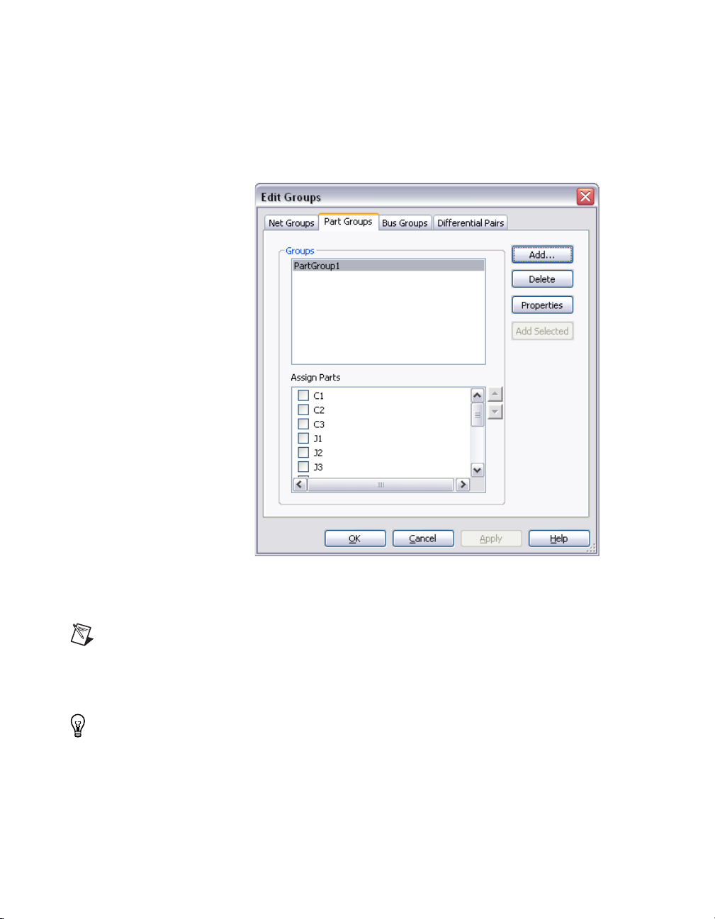
Chapter 3 Setting Up a Design
6. Click OK to return to the Part Groups tab. The newly created group
appears in the Groups list.
7. Highlight the new group to display a list of parts you can add to the
group in the Assign Parts list, as shown in the example below.
8. Click checkboxes beside the desired parts in the Assign Parts list and
click Apply to add them to the group.
Note You cannot assign a part to more than one group. Therefore, parts that are already
assigned to another group do not appear in the Assign Nets list.
9. Click OK to close the Edit Groups dialog box.
Tip When adding parts to a Part Group, you can select parts on the workspace and then
click Add Selected in the Part Groups tab—the selected parts are added to the group.
NI Ultiboard User Manual 3-14 ni.com
Page 91

Complete the following steps to edit a part group:
1. Select Tools»Group Editor to display the Edit Groups dialog box.
2. Select the Part Groups tab.
3. Highlight the desired group in the Groups list.
4. Change the part assignments as desired and click Apply.
5. Optionally, highlight the desired group in the Groups list and click the
Properties button to display the Change group settings dialog box.
6. Make the required changes in the Group Settings area and click OK.
Note Refer to the Change Group Settings dialog box and Net Group Settings sections for
more information.
Complete the following steps to delete a group:
1. Select Tools»Group Editor to display the Edit Groups dialog box.
2. Select the Part Groups tab.
3. Highlight the desired group in the Groups list and click Delete.
Working with Bus Groups
Set up a bus group for traces that you wish to route as closely together as
possible.
Chapter 3 Setting Up a Design
Complete the following steps to create a bus group:
1. Select Tools»Group Editor to display the Edit Groups dialog box.
2. Click the Bus Groups tab.
3. Click Add. The Add group dialog box appears.
4. Enter the desired name and click OK.
5. The newly created group appears in the Assign Nets list.
6. Highlight the new group to display a list of nets you can add to the
group in the Assign Nets list, as shown in the example below.
© National Instruments Corporation 3-15 NI Ultiboard User Manual
Page 92
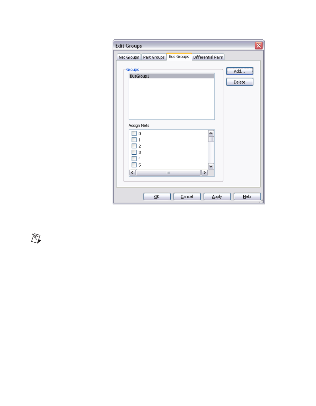
Chapter 3 Setting Up a Design
7. Click checkboxes beside the desired nets in the Assign Nets list and
click Apply to add them to the group.
Note You cannot assign a net to more than one group. Therefore, nets that are already
assigned to another bus group do not appear in the Assign Nets list.
8. Click OK to close the Edit Groups dialog box.
Complete the following steps to edit a bus group:
1. Select Tools»Group Editor to display the Edit Groups dialog box.
2. Select the Bus Groups tab.
3. Highlight the desired group in the Groups list.
4. Change the net assignments as desired and click Apply.
Complete the following steps to delete a group:
1. Select Tools»Group Editor to display the Edit Groups dialog box.
2. Select the Bus Groups tab.
3. Highlight the desired group in the Groups list and click Delete.
NI Ultiboard User Manual 3-16 ni.com
Page 93

Working with Differential Pairs
Complete the following steps to create a differential pair:
1. Select Tools»Group Editor to display the Edit Groups dialog box.
2. Click the Differential Pairs tab.
3. Click Add. The Add group dialog box appears.
4. Enter the desired name and click OK. The Change group settings
dialog box appears.
5. Change the settings in the Group Settings area as desired.
Note Refer to the Change Group Settings dialog box and Differential Pair Settings
sections for more information.
6. Click OK to return to the Differential Pairs tab. The newly created
group (differential pair) appears in the Groups list.
7. Highlight the new group to display a list of nets you can add to the
group in the Assign Nets list, as shown in the example below.
Chapter 3 Setting Up a Design
© National Instruments Corporation 3-17 NI Ultiboard User Manual
Page 94

Chapter 3 Setting Up a Design
Note You cannot assign a net to more than one differential pair. Therefore, nets that are
already assigned to another differential pair do not appear in the Assign Nets list.
Note Refer to the Change Group Settings dialog box and Differential Pair Settings
sections for more information.
8. Click two checkboxes beside the desired nets in the Assign Nets list
and click Apply to add them to the group.
9. Click OK to close the Edit Groups dialog box.
Complete the following steps to edit a bus group:
1. Select Tools»Group Editor to display the Edit Groups dialog box.
2. Select the Differential Pairs tab.
3. Highlight the desired group in the Groups list.
4. Change the net assignments as desired and click Apply.
5. Optionally, highlight the desired group in the Groups list and click the
Properties button to display the Change group settings dialog box.
6. Make the required changes in the Group Settings area and click OK.
Complete the following steps to delete a group:
1. Select Tools»Group Editor to display the Edit Groups dialog box.
2. Select the Differential Pairs tab.
3. Highlight the desired group in the Groups list and click Delete.
Change Group Settings dialog box
Access this dialog box from the Edit Groups dialog box. Refer to the
Working with the Group Editor section for more information.
Use this dialog box to change the group settings for net groups, part groups,
and differential pairs.
The options found in this dialog box depend on the type of group. Refer to
the following sections for more information:
• Net Group Settings
• Part Group Settings
• Differential Pair Settings
NI Ultiboard User Manual 3-18 ni.com
Page 95

Chapter 3 Setting Up a Design
Net Group Settings
For net groups, the following Group Settings are available:
• Group Name
• Clearance Settings
• Trace Width Settings
• Trace Length Settings
• Routing Layers
• Routing Priority
• Locked
As well as setting the clearance for a net group, you can set clearances for
individual nets within that group. You can, for example, set the clearance
for the net group to 10 mils, and the clearance for two or more nets within
that group to 5 mils. In this case, if any net from the group comes within 10
mils of any element that is not in the net group, a DRC error is generated.
If one of the traces that you set to a 5 mils clearance moves to 5 mils or less
from one of the other traces with the 5 mils clearance setting, a DRC error
occurs.
Note Set individual trace clearances in the Nets tab of the Spreadsheet View. To do this,
select the desired trace, and locate the Trace Clearance column. Highlight Use Group
Settings and type in the desired clearance for that trace. You can also edit a trace’s
clearance from the General tab of its properties dialog box.
For information on any setting, select it in the Group Settings list. A
description appears in the field at the bottom of the dialog. You may need
to make the dialog box larger to view some of the descriptions. Do this by
dragging the dialog’s lower-right corner.
Part Group Settings
For part groups, the following Group Settings are available:
• Group Name
• Clearance Settings
• Part Spacing Settings
• Pin & Gate Swapping Settings
© National Instruments Corporation 3-19 NI Ultiboard User Manual
Page 96

Chapter 3 Setting Up a Design
For information on any setting, select it in the Group Settings list. A
description appears in the field at the bottom of the dialog. You may need
to make the dialog box larger to view some of the descriptions. Do this by
dragging the dialog’s lower-right corner.
Differential Pair Settings
For differential pairs, the following Group Settings are available:
• Length Constraints
• Space Constraints
For information on any setting, select it in the Group Settings list. A
description appears in the field at the bottom of the dialog. You may need
to make the dialog box larger to view some of the descriptions. Do this by
dragging the dialog’s lower-right corner.
NI Ultiboard User Manual 3-20 ni.com
Page 97

Working with Parts
The following sections explain how to work with parts as you create and
edit designs. It covers the ways that you can place parts on the board, as
well as the tools included to help you with part location and placement. It
also includes information on Ultiboard’s parts database, and editing the
parts in the database and on the board.
Some of the described features may not be available in your edition of
Ultiboard. Refer to the NI Circuit Design Suite Release Notes for a list of
the features in your edition.
Placing Parts
You can place parts on the design:
• by dragging them from outside the board outline. Refer to the
Dragging Parts from Outside the Board Outline section for more
information.
• by using the Spreadsheet View. Refer to the Using the Parts Tab in
the Spreadsheet View section for more information.
• by importing a netlist. Refer to the Creating a Design from a Netlist
File section of Chapter 2, Beginning a Design, for more information.
• by selecting parts from the database. Refer to the Placing Parts from
the Database section for more information.
4
Note Before placing a part, make sure that you are on the layer where the part is to be
placed. Refer to the Accessing Layers section of Chapter 3, Setting Up a Design, for more
information.
Dragging Parts from Outside the Board Outline
By default, parts are placed outside the board outline when you open a
netlist from Multisim or another schematic capture program. These can be
dragged to the appropriate location on the board.
© National Instruments Corporation 4-1 NI Ultiboard User Manual
Page 98
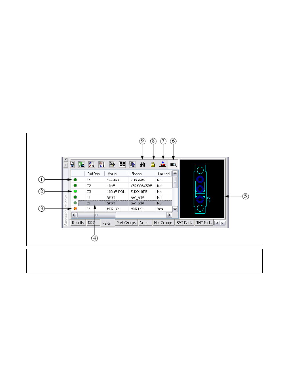
Chapter 4 Working with Parts
Complete the following steps to drag a part from outside the board outline:
1. Click on the part and drag it to the appropriate location. The placed part
remains highlighted.
2. Click anywhere on the workspace, or right-click, to de-select the part.
Using the Parts Tab in the Spreadsheet View
The Parts tab in the Spreadsheet View shows a list of all the parts in your
design.
The Parts tab is also where you select parts, lock parts so they cannot be
accidentally moved, and place parts on the board. It also contains functions
to help you find parts on the board, and preview a selected part.
1 Dark Green Indicator
2 Bright Green Indicator
3 Orange Indicator
4 Selected Part
5 Preview of Selected Part
6 Show or Hide Preview Button
7 Start Placing Unpositioned Parts
Button
8 Lock Selected Parts Button
9 Find and Select Part Button
The dark green indicator (1) shows that the part has not been placed within
the board outline. If all parts’ indicators are dark green, there may be no
board outline defined.
The bright green indicator (2) shows that the part has been placed within
the board outline.
The orange indicator (3) shows that the part has been locked in place.
NI Ultiboard User Manual 4-2 ni.com
Page 99

Chapter 4 Working with Parts
The selected part (4) appears in the preview area (5). Deselect the Show or
Hide Preview button (6) if you do not wish to see the preview.
Use the Start Placing the Unpositioned Parts button (7) to place unplaced
parts.
Use the Lock Selected Parts button (8) if you do not want a part to be
moved.
Use the Find and Select Part button (9) to quickly locate a part on the
design.
Note Refer to the Spreadsheet View section of Chapter 1, User Interface, for information
about the other buttons in the Spreadsheet View.
Using the Parts Tab to Place Parts
Complete the following steps to place a single part on the board:
1. Click-and-drag the part from the list to the design. The selected part is
attached to the pointer as you move it over the board.
2. Release the mouse button to drop the part onto the board. The part can
then be adjusted or moved further into position as needed. Refer to the
Tools to Assist Part Placement section for more information about
moving parts and adjusting their placement.
Complete the following steps to place a series of parts on the board using
the Parts Sequencer:
1. Click an unplaced part in the list (a part with a dark green button). The
Start Placing the Unpositioned Parts button is activated on the Parts
tab.
2. Click the Start Placing the Unpositioned Parts button.
3. Move the pointer over the board. The selected part is attached to the
pointer as you move it over the board.
4. When the part is in position, click to drop it on the board. The next part
in the list appears on the mouse pointer.
5. Continue clicking to drop a part and pick up the next until you have
placed as many as desired.
6. Right-click to drop the last part or to cancel the action.
Parts that you place this way can then be adjusted or moved as necessary.
Refer to the Tools to Assist Part Placement section for more information
about moving parts and adjusting their placement.
© National Instruments Corporation 4-3 NI Ultiboard User Manual
Page 100

Chapter 4 Working with Parts
Using the Parts Tab for Other Functions
The Parts tab of the Spreadsheet View can also be used to select a part,
lock parts in their current position, find and select a part, or preview a part.
To select a part using the Parts tab, double-click the part in the list. The part
appears selected in the design.
Complete the following steps to lock and unlock parts:
1. Click a part in the list to select it. To select multiple parts, click one
part, hold the Shift key down, then click the last part you want to select.
The two parts that you clicked, and any parts listed between them, are
now selected.
2. Click the Lock the Selected Part button to lock all selected unlocked
parts or to unlock the selected locked parts.
Complete the following steps to find a part in the design:
1. Click the part in the list.
2. Click the Find and Select the Part button. The view zooms in on the
part, which appears selected.
Complete the following steps to preview a part:
1. Click the Preview button to toggle the Preview function on, if
required.
2. Click the part in the list. A picture of the part displays.
You can use the Parts tab to place parts that are not on the board but are
listed in the Parts tab. Parts listed on the tab are either placed on the board
or have been imported but not yet placed within the board outline. Parts that
are listed in the Parts tab but are not on the board are indicated with a dim
button, while parts that have been placed on the board are indicated with a
bright button.
Note Refer to the Spreadsheet View section of Chapter 1, User Interface, for information
about the other buttons in the Spreadsheet View.
NI Ultiboard User Manual 4-4 ni.com
 Loading...