

Page 1
USER GUIDE
SLSC-12101
Prototyping Module
RADIAL
SELECTOR
CONNECTOR J1
CONNECTOR J2
SLSC -12101
POWER
READY
PROTOTYPING MODULE
Overview
The SLSC-12101 is a prototyping module intended to help SLSC module developers quickly
prototype designs. The module is Level-2 compatible, but can be Level-1 compatible if you
configure the rear I/O signals properly.
The SLSC-12101 features a MAX V CPLD as a module controller, which is pre-programmed
to provide basic access to the board peripherals. The MAX V CPLD is divided into four banks,
and the I/O for each is routed to its own region in the prototyping area. Each bank may have
Page 2

independent voltage settings to allow the use of different digital standards supported by the
CPLD. Custom circuitry in the prototyping area has access to 24 V and 3.3 V rails from the
backplane, 5 V from the auxiliary power supply and corresponding bank power supply. Two of
the regions of the prototyping area, Bank 1 and Bank 2, include connections to two 44-pin
DSUB connectors in the front panel. A fifth region in the prototyping area, labeled RTI,
provides additional space to access the upper rear I/O connectors.
The peripherals designed into the SLSC-12101 board include two front panel LEDs (which
follow the recommendations of the SLSC Design Guidelines), a 16-position rotary switch, four
temperature sensors, and 17 ports 8-bit wide routed to their corresponding banks in the
prototyping area.
Additionally, to ease debugging and prototyping, a JTAG header compatible with Altera's USB
Blaster pinout is populated on the board which allows you to program the CPLD with a
custom design. A MICTOR connector exists between the CPLD and the SLSC connector to
allow monitoring of the SLSC interface signals using a logic analyzer such as the one on NI
VirtualBench.
Note All modifications to this module must comply with the Switch Load and
Signal Conditioning Module Design Specifications. It is the user's responsibility to
make sure that the product is modified and used in a way that complies with local
rules, regulations, and best practices.
Note All specifications and certifications in the manual apply only to the unaltered
product as provided by National Instruments. Any changes to the product invalidate
these specifications and certifications.
Related Documentation
This user guide assumes you have access to the documentation of the SLSC Module
Development Kit (MDK) and that you are familiar with the following documents:
• Switch Load and Signal Conditioning Module Design Specifications—Specifications
SLSC modules must abide in order to be compatible with SLSC systems.
• SLSC Design Guidelines—Describes best practices recommended for SLSC modules.
• SLSC-12101 Schematic—Schematic of the SLSC-12101 prototyping module.
• SLSC-12101 Specifications—Specifications of the unaltered SLSC MDK.
Other Files Available for the SLSC-12101 Module
These files are included in the SLSC Example Modules Files .zip file of the SLSC MDK.
• Module Controller VHDL code—Slsc12101Top.vhd, PkgEdBlock.vhd,
PkgRevision.vhd, PkgSlsc12101Registers.vhd, PkgSlscProtocol.vhd,
EdBlock.vhd, Interrupt.vhd, IoPort.vhd, Leds.vhd,
SpiChannelSelect.vhd, Control.vhd, CrcGen.vhd, ShiftRegister.vhd,
Spi.vhd
• Module Controller Quartus project files—SlscCpldTop.qpf, SlscCpldTop.qsf,
SlscCpldTop.sdc, SlscCpldTop.pof
• SLSC-12101 Capabilities files—SLSC-12101.bin, SLSC-12101.json
2 | ni.com | SLSC-12101 User Guide
Page 3

• 2D Mechanical Drawings and 3D Models
• SLSC-12101 PCB Drawing
Required Software
• NI LabVIEW 2015 or newer
• NI-SLSC driver
• To customize the CPLD: Quartus Design software, found on Quartus Software's website
1
• To customize the Flash: createNvmemImage.py, included in the SLSC MDK files
Other Files
• SLSC-12101.vi—Example VI to access the SLSC-12101 properties.
Getting Started with the SLSC-12101
The SLSC-12101 can be inserted into an SLSC chassis and used the way it is shipped.
Note The SLSC chassis and SLSC modules do not support hot plug-in. The entire
chassis must be powered down when a module is installed or removed.
1. Ensure the CPLD power supplies are properly set.
After taking the module out of its packaging, check that three jumpers are inserted
between pins 5 and 10 of headers W2, W3, and W4. This ensures that the voltage is set to
3.3 V for the CPLD I/O banks 2, 3, and 4.
1
Quartus Design Software is offered in a variety of editions with different features and price ranges.
Refer to the Quartus Software website for more information.
SLSC-12101 User Guide | © National Instruments | 3
Page 4
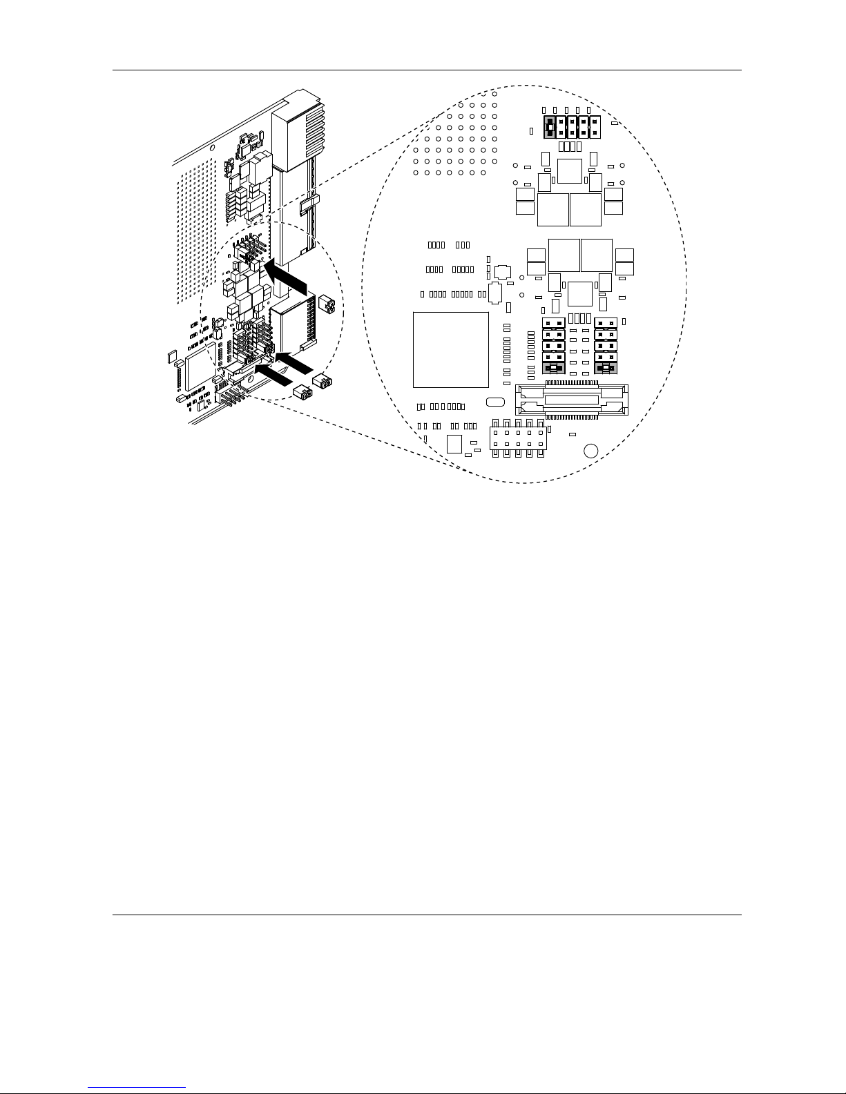
Figure 1. Jumper Configuration
2. Install the module in the SLSC chassis.
Power off the SLSC chassis and then insert the module into an available slot. If you are
using the JTAG connector to program the CPLD or MICTOR cable to a logic analyzer,
leave one empty slot to the right of the module for cable routing. Connect the cable(s)
before inserting the module in the chassis.
3. Power up the chassis.
As soon as the chassis is powered up, the power LED of the front panel of the
SLSC-12101 should be lit green. The chassis will boot-up and start querying the slots for
module presence. Once the module is detected, the Ready LED should be lit green.
4. Access the module's properties and physical channels.
Use a host computer with LabVIEW and the NI-SLSC driver installed, and connected to
the same network as the SLSC chassis. Open SLSC-12101.vi. This VI gives you
access to the properties and physical channels that control the peripherals of the module.
You can control the LEDs, read the value dialed in the rotary switch, and access all the
DIO going to the prototyping area.
Description of the SLSC-12101
Mechanical Features
Unless otherwise noted, mechanical attributes and restrictions such as maximum component
height are defined in the Switch Load and Signal Conditioning Module Design Specifications.
4 | ni.com | SLSC-12101 User Guide
Page 5
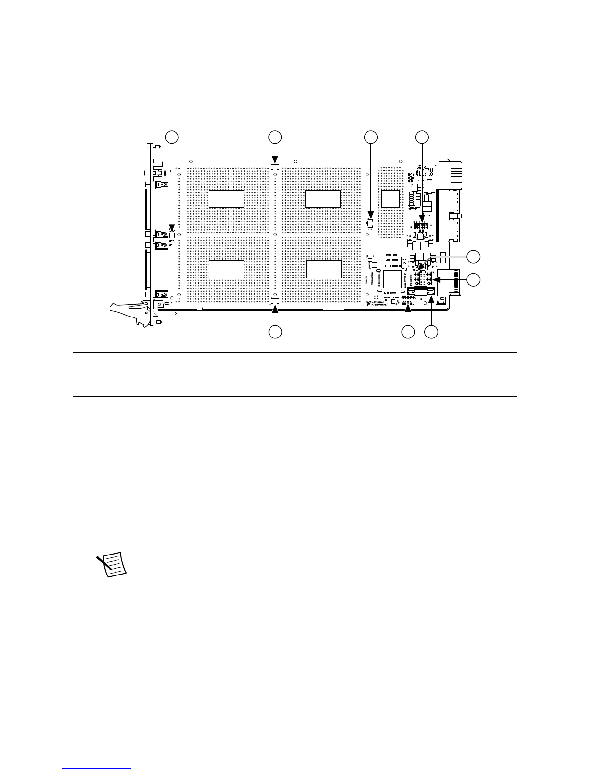
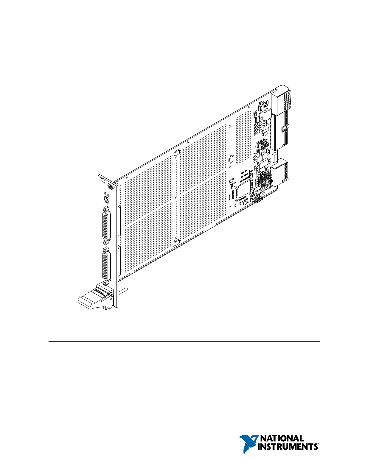
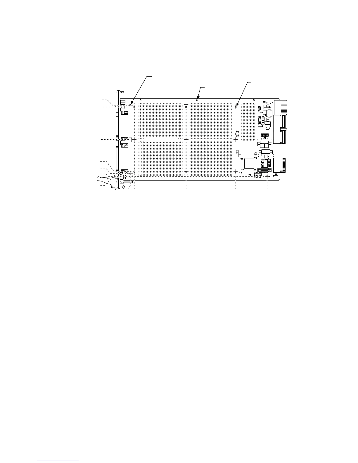
Top View and Main Components
The following figure shows the top view of the SLSC-12101 module and highlights its most
relevant components.
Figure 2. SLSC-12101 Top View
1 1 1 2
BANK 1
BANK 2
BANK 3
RTI
BANK 4
1
6
5
4
3
1. Temperature Sensor (4x)
2. Voltage Configuration Header - Bank 2
3. Voltage Configuration Header - Bank 4
4. Voltage Configuration Header - Bank 3
5. MICTOR Connector (for NI VirtualBench)
6. JTAG Header (CPLD Programming)
• Prototyping area—The biggest area of the board is used for prototyping and is divided
into five areas filled with thru-hole grids. These grids can be used with standard 0.10"
headers, or may have wires or thru-hole components soldered to them. The prototyping
area provides access to the majority of the CPLD I/O, the front and rear connectors,
power supplies, and ground.
• Module controller—Implemented in a MAX V CPLD, handles the communication with
the SLSC chassis and controls the peripherals.
• Variable power supplies for CPLD Banks 2, 3, and 4—These power supplies can be set
by the developer by placing the jumper of the corresponding header in the correct
position.
Note The jumpers must be set before powering the module and should not be
changed once the system is powered.
• Front and rear connectors—The connectors on the front panel and those facing the RTI
area are the same as those recommended in the Switch Load and Signal Conditioning
Module Design Specifications and in the SLSC Design Guidelines.
• Rotary switch—The position of the rotary switch can be accessed by standard SLSC
properties.
• Front panel LEDs—The LEDs can be controlled through standard SLSC properties.
• Temperature sensors—4x ADT7310 are connected to the CPLD.
SLSC-12101 User Guide | © National Instruments | 5
Page 6

Front Panel
The following figure shows the front view of the module and highlights its features.
Figure 3. Front Panel
CONNECTOR J1 CONNECTOR J2
SLSC -12 101
PROTOTYPING MODULE
POWER
READY
RADIAL
SELECTOR
5
6
7
8
9
3
2
1
4
1. SLSC Interface Compatibility Glyph—This
indicates chassis compatibility type.
2. SLSC Rear I/O Compatibility Glyph—This
indicates RTI compatibility type, which is left blank
for customization. See the Switch Load and Signal
Conditioning Module Design Specifications for
more information.
3. Top Module Mounting Screw
4. LEDs—See Front Panel LEDs section for more
details.
5. Rotary Switch
6. Connector J1 (high-density 44-position DSUB)
7. Connector J2 (high-density 44-position DSUB)
8. Injector/Ejector Handle
9. Bottom Module Mounting Screw
6 | ni.com | SLSC-12101 User Guide
Page 7
Connectors
The SLSC-12101 is designed with the front and rear connectors recommended in the Switch
Load and Signal Conditioning Module Design Specifications and SLSC Design Guidelines.
The module has the proper connectors for meeting Level-1 compatibility, but you must
properly configure signals to and from these connectors in the RTI prototyping area. Refer to
the Switch Load and Signal Conditioning Module Design Specifications for compatibility
requirements.
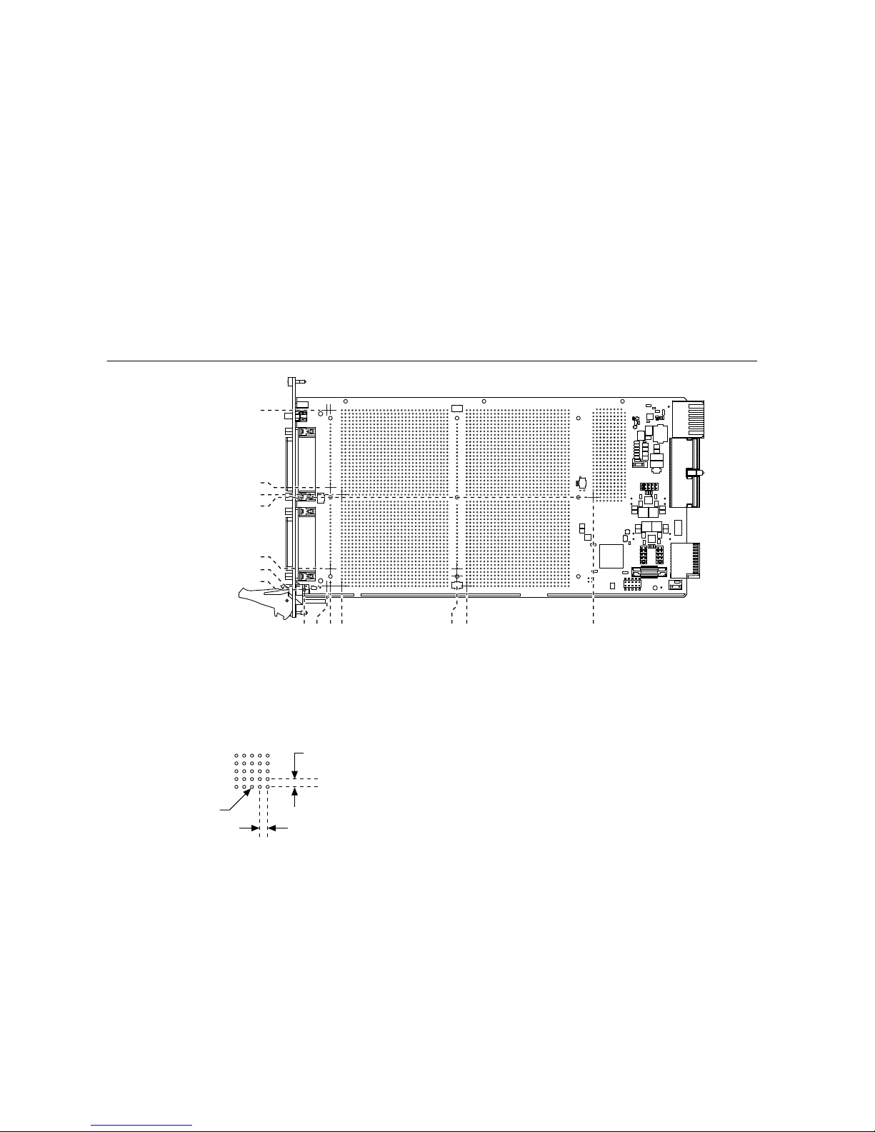
Prototyping Area Hole Arrays
The following figure provides information about the arrays of holes found in the prototyping
areas. These holes may be used for direct soldering of components and wires, or for attaching
standard headers to connect to jumpers or secondary PCBs.
Figure 4. Prototyping Area Hole Array Details
2.54 mm
(0.100 in.)
2.54 mm
(0.100 in.)
Ø 1.02 mm
(0.040 in.)
plated
Prototyping Area
Hole Array Detail
129.54 mm (5.100 in.)
71.12 mm (2.800 in.)
68.58 mm (2.700 in.)
66.68 mm (2.625 in.)
15.24 mm (0.600 in.)
2.54 mm (0.100 in.)
0.0 mm (0.0 in.)
0.0 mm (0.0 in.)
16.51 mm (0.650 in.)
19.05 mm (0.750 in.)
27.31 mm (1.075 in.)
117.48 mm (4.625 in.)
208.92 mm (8.225 in.)
110.49 mm (4.350 in.)
Mounting Holes
The following figure provides information about the location and size of mounting holes. The
three holes across the top of the PCB are reserved for future extension hardware. See the
Switch Load and Signal Conditioning Module Design Specifications for information about
placement restrictions around these holes.
SLSC-12101 User Guide | © National Instruments | 7
Page 8
Twelve other mounting holes are provided: three larger holes in the corners of the board, and
nine smaller holes forming a grid in the center of the board in the prototyping area. These may
be used at the discretion of the module developer to provide mechanical fixturing as needed,
including shields, brackets, or mounting standoffs for custom secondary PCBs.
Figure 5. Mounting Hole Sizes and Locations
127.00 mm
(5.000 in.)
3X 66.68 mm
(2.625 in.)
3X 9.53 mm
(0.375 in.)
6.35 mm (0.250 in.)
0.0 mm (0.0 in.)
1.27 mm (0.50 in.)
253.54 mm (9.982 in.)
3X Ø 3.18 mm (0.125 in.)
Non-plated Thru Holes
3X Holes Reserved
for Extension HW
9X Ø 2.69 mm (0.106 in.)
Non-plated Thru Holes
3X 110.49 mm (4.350 in.)
3x 198.12 mm (7.800 in.)
0.0 mm (0.0 in.)
2X 11.94 mm (0.470 in.)
3X 19.05 mm (0.750 in.)
3X 123.83 mm
(4.875 in.)
Electrical Features
The Input Rails and Fuse
The module takes its power from the 24 V and 3.3 V provided by the chassis. 3.3 V is only
used for the VCCO of Bank 1 and other support circuitry such as the 40 MHz oscillator, flash
memory, and thermal sensors. The rest of the banks and the core power used by the CPLD
come from cascaded switcher regulators powered from an auxiliary 5 V supply connected to
the 24 V rail. Banks 2-4 can be set to different values to allow you to use different digital
standards available in the CPLD.
All the 24 V, 5 V, and Banks 1-4 VCCOs are available in the prototyping area to be used by
the support circuitry required by your design. You should make sure your design does not
exceed the power limitations of these rails.
As required by the Switch Load and Signal Conditioning Module Design Specifications, the
24 V power supply is protected by a 3.5 mA fuse. See the SLSC-12101 Bill of Materials for
more information.
8 | ni.com | SLSC-12101 User Guide
Page 9

Auxiliary 5 V Power Supply
The programmable power supplies and the CPLD core power supply of 1.8 V are all powered
by an auxiliary 5 V power supply which is powered from the 24 V provided by the SLSC
chassis. This 5 V power supply is also available in the prototyping area. The power supply can
support a maximum of 6 A.
Variable Voltage Power Supplies
The MAX V supports VCCIO of 1.2 V, 1.5 V, 1.8 V, 2.5 V, and 3.3 V in order to use several
I/O standards. The SLSC-12101 has user-configurable power supplies for three of the four
CPLD banks. The voltages are set by placing a jumper in the corresponding header connecting
the pair labeled with the desired voltage. The jumper should be placed on the board before the
module is inserted in the SLSC chassis.
Once a voltage is set for a bank, all the signals on that bank need to use an I/O standard
supported by that voltage. For more information about the supported I/O standards and rules to
interconnect I/O standards with the MAX V CPLD, refer to Altera's MAX V Device Handbook.
The voltages of all the banks are also routed to the prototyping area to allow the circuits built
there to use it. The maximum current that can be withdrawn from each bank depends on the
maximum current the source can provide, as well as the estimated current used by the CPLD.
Bank 1 is powered directly from the SLSC chassis and, by SLSC Specification 1.0, the module
shall not withdraw more than 400 mA. Banks 2-4 take their power from 24 V on-board power
supplies and can provide up to 2 A. In addition to the limitations imposed by the current limits
on the different rails on the module, you should also consider the power dissipation limitations
as defined in the Switch Load and Signal Conditioning Module Design Specifications.
Table 1. Bank Rail Available Voltages and Current Limits
Bank Available Voltages Maximum Current
1 3.3 V fixed, provided by the SLSC backplane 400 mA
2 1.2 V, 1.5 V, 1.8 V, 2.5 V, 3.3 V 2 A
3 1.2 V, 1.5 V, 1.8 V, 2.5 V, 3.3 V 2 A
4 1.2 V, 1.5 V, 1.8 V, 2.5 V, 3.3 V 2 A
Module Controller
The SLSC-12101 Module Controller is implemented using Altera's MAX V
5M1270ZF256I5N. The CPLD is shipped pre-programmed with the compiled version of the
Slsc12101Top.vhd design also included in the SLSC Module Development Kit. The
controller's default image already implements the EdBlock.vhd design to handle SLSC
Frames and the required compliance registers as described in Chapter 8 of the Switch Load
and Signal Conditioning Design Specifications. Through the ED Mode, the controller can
access the peripherals present on the board, such as the front panel LEDs, the front panel
rotary switch, and 17 8-bit I/O ports routed from the CPLD to the prototyping area.
SLSC-12101 User Guide | © National Instruments | 9
Page 10

CPLD Programming
The SLSC-12101 has a header that directly connects to Altera's USB Blaster to quickly
program the CPLD with a custom design. You can use the SLSC12101Top.vhd file provided
in the SLSC Module Development Kit as a starting point for development.
Front Panel LEDs
The SLSC-12101 has Power and Ready LEDs as recommended in section 3.6 of the Switch
Load and Signal Conditioning Design Specifications. The LEDs can be lit red, yellow, and
green—continuously or blinking—so you can implement the information in Table 3-1 of that
specification. The default module controller behavior implements the Power Solid Green and
the Ready Solid Green as recommended in Table 3-1.
The Leds.vhd component provided with the SLSC Module Development Kit implements an
easy interface to control the LEDs through the NI.ReadyLedColor, NI.ReadyLedMode,
NI.PowerLedColor, and NI.PowerLedMode properties described in the capabilities file
included as part of the kit.
Rotary Switch
The 16-position, 4-bit rotary switch on the front panel is accessible from the CPLD. The value
can be accessed through the SLSC API using the NI.RotarySwitch property.
SI5356A Clock Generator
The module has pads for you to add an SI5356A clock generator should you need more clocks
in your design. This clock generator can provide up tp four different frequencies on eight pins.
Each output clock has two pins. In the SLSC-12101, one pin is routed to a global clock pin of
the CPLD, and another pin is routed to the prototyping area. For more information on the
routing of these clocks to the prototyping area, refer to the pinout sections and the
SLSC-12101 Schematic.
Design Development, Characterization, and
Debugging
The SLSC-12101 was designed to provide an easy way to prototype SLSC modules in
development. Use the resources provided by the SLSC chassis, the module controller, and the
connectors to help you implement your design, to characterize some aspects such as power
consumption and dissipation, as well as for increased visibility for diagnostics.
Prototyping Area
Most of the board consists of the prototyping areas, which are filled with hole arrays of
2.54 mm (0.100 in.) pitch. These are all plated holes to ease soldering. There are five main
grid areas for prototyping: Bank 1, Bank 2, Bank 3, Bank 4, and RTI. Each bank gives access
to signals of the corresponding bank on the CPLD as well as to the corresponding bank
VCCO. Banks 1 and 2 also provide access to the front panel connectors.
10 | ni.com | SLSC-12101 User Guide
Page 11

The RTI grid contains holes connected to the rear I/O connectors, XJ02 and XJ03, along with
several grounds, access to the 24 V supply from the backplane, and two pairs of holes
connected to each of the bank rails.
Each of the five grids has its own coordinate system. Rows are numbered from top to bottom,
and columns are marked with letters from left to right. Hole A1 is always at the top-left corner.
These coordinates are referenced in this document.
For a detailed assignment of the hole arrays, refer to the SLSC-12101 pinout sections of this
manual.
Power Consumption Validation
To ease the validation of power consumption in the module, you can monitor the power rails.
The 24 V and 3.3 V rails provided by the backplane go through bridge resistors that can be
removed so that current measurements can be performed. Resistor R 16 connects the
backplane 24 V rail to the module, and W1 provides two holes to connect a bypass cable for
current measurement or an external power supply. The 3.3 V rail uses resistor R168 as the
bridge and W6 as the bypass holes.
Figure 6. 24 V Bridge Resistor and Bypass Holes
The power supplies for banks 2-4 do not have a bridge resistor. Instead they are routed in such
a way that they have a thick trace on the primary side of the board so it can be cut. Holes exist
for bypass cables. A dotted line with a label of the bank it supplies power to indicates where
the trace should be cut. See the following figures.
Figure 7. Bank 2 Voltage Setting Header and Dotted Lines for Power Trace Cutting
SLSC-12101 User Guide | © National Instruments | 11
Page 12
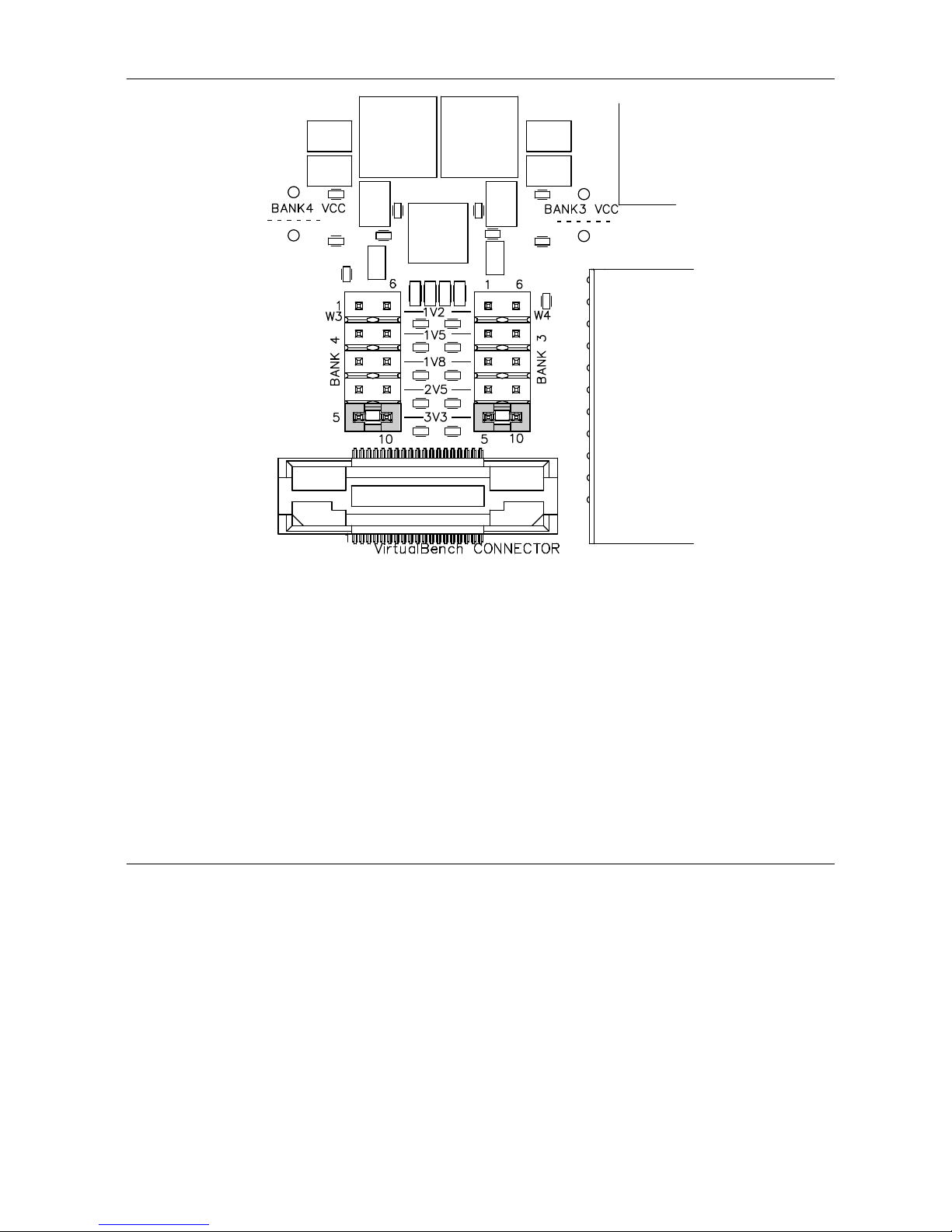
Figure 8. Bank 3 and Bank 4 Voltage Setting Header
Logic Analyzer Connector
A 43-pin MICTOR Connector is placed between the CPLD and SLSC Interface connector for
direct monitoring of the signals using a logic analyzer. In addition to the SLSC signals, 17
debug lines are connected directly from the CPLD to the connector. In the shipping CPLD
image, two of these lines are controlled by DIO ports, one line is a copy of the internal 40
MHz clock, and 14 lines are only driven to GND. You can use all 17 lines to monitor internal
signals of your design. See pinout sections for more information on the signal routing to this
connector.
Description of the Module Controller HDL
General Architecture
The SLSC-12101 Module Controller instantiated in the MAX V CPLD is implemented in
VHDL. The top-level file is Slsc12101Top.vhd. The design uses an instance of EdBlock
(EdBlock.vhd) to handle the communication between the SLSC chassis and the Module
Controller. The design features an SPI Channel selector which can be used for future SPI
channel expansion in the SLSC architecture. This channel expansion can be used in this
module to access temperature sensors in the prototyping area.
12 | ni.com | SLSC-12101 User Guide
Page 13
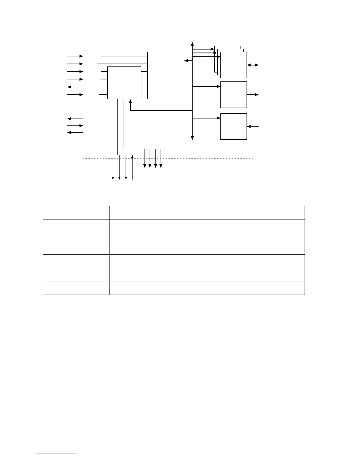
Figure 9. SLSC-12101 Block Diagram
Prototyping
Area Banks
Front Panel
LEDs
Temperature
Sensors
Alarms
Other Internal
Registers
4x Temp Sensor
Channels
Rdy/Rst#
SLSC-12101 Controller
(5M1270ZF25615N)
SpiClk
SpiMOSI
ED_SS#
ID_SS#
Int#
TTM
TFM
Id SPI Channel
MISO
ID_SS
SpiClk
SpiMosi
SpiMISO
RegInterface Bus
IoPort.vhd
Interrupt.vhd
Interrupt
LEDs
17x I/O
Ports
EdBlock
SPI
Channel
Select
SpiChannelSelect.vhd
EdBlock RegInterface
(cRegPortOut, cRegPortIn)
EdBlock.vhd
Spi.vhd
Control.vhd
CrcGen.vhd
SlscCpldTop.vhd
Table 2. Main Files Included in the Module Development Kit (Without Dependencies)
File Name Notes
Slsc12101Top.vhd Top-level file which can be compiled to generate a programming
bitfile for the CPLD
SlscCpldTop.qpf Quartus II project file
SlscCpldTop.qsf Quartus II settings file
SlscCpldTop.sdc Constraints file
SlscCpldTop.pof Programming bitfile
EdBlock Implementation
The EdBlock abstracts out the frames received through the SPI lines of the SLSC interface
into a register port. You can use it to easily implement registers in your design by calling the
RegisterRead and RegisterWrite functions declared in the PkgEdBlock.vhd file. You will
only need to focus on implementing a digital circuit that converts these register accesses into
useful control and monitor signals in your design.
The Error Detection block is implemented in VHDL and consists of the following files:
SLSC-12101 User Guide | © National Instruments | 13
Page 14
File Name Notes
EdBlock.vhd Top-level file of the component which can be instantiated
in a CPLD top-level design. It handles incoming SLSC
frames, handles errors when detected, and executes the
corresponding register access when valid frames are
received.
Spi.vhd, Control.vhd,
CrcGen.vhd,
ShiftRegister.vhd
Sub-components of the EdBlock.
PkgEdBlock.vhd Contains the RegisterRead and RegisterWrite functions
and records to easily implement registers in a top-level
design.
PkgSlscProtocol.vhd Contains constants relevant to the SLSC Specifications
1.0.
Error Detection Block Instantiation
You can instantiate the Error Detection block in your design as follows:
Variable Voltage Power Supplies
The MAX V supports VCCIO of 1.2 V, 1.5 V, 1.8 V, 2.5 V, and 3.3 V in order to use several
I/O standards. The SLSC-12101 has user-configurable power supplies for three of the four
CPLD banks. The voltages are set by placing a jumper in the corresponding header connecting
the pair labeled with the desired voltage. The jumper should be placed on the board before the
module is inserted in the SLSC chassis.
Once a voltage is set for a bank, all the signals on that bank need to use an I/O standard
supported by that voltage. For more information about the supported I/O standards and rules to
interconnect I/O standards with the MAX V CPLD, refer to Altera's MAX V Device Handbook.
The voltages of all the banks are also routed to the prototyping area to allow the circuits built
there to use it. The maximum current that can be withdrawn from each bank depends on the
maximum current the source can provide, as well as the estimated current used by the CPLD.
Bank 1 is powered directly from the SLSC chassis and, by SLSC Specification 1.0, the module
shall not withdraw more than 400 mA. Banks 2-4 take their power from 24 V on-board power
14 | ni.com | SLSC-12101 User Guide
Page 15

supplies and can provide up to 2 A. In addition to the limitations imposed by the current limits
on the different rails on the module, you should also consider the power dissipation limitations
as defined in the Switch Load and Signal Conditioning Module Design Specifications.
Table 3. Bank Rail Available Voltages and Current Limits
Bank Available Voltages Maximum Current
1 3.3 V fixed, provided by the SLSC backplane 400 mA
2 1.2 V, 1.5 V, 1.8 V, 2.5 V, 3.3 V 2 A
3 1.2 V, 1.5 V, 1.8 V, 2.5 V, 3.3 V 2 A
4 1.2 V, 1.5 V, 1.8 V, 2.5 V, 3.3 V 2 A
Peripheral Implementations
Along with EdBlock, the Module Development Kit provides a few examples of useful
instances that can be used directly with EdBlock to implement common functionality to
interact with a wide range of devices that can be placed in the prototyping area or with
peripherals already present on the board.
File Name Notes
Interrupt.vhd Customizable entity that implements interrupts which follow
the Switch Load and Signal Conditioning Design Specifications
and are compatible with the EdBlock register map.
IoPort.vhd Customizable entity that implements digital I/O compatible
with the EdBlock register map.
Leds.vhd LED controller compatible with the EdBlock register map that
allows the control of bi-color LEDs for the SLSC-12101.
SpiChannelSelect.vhd Customizable entity that allows switching SPI channels for all
the slaves in the SLSC-12101.
Digital Input and Output
The IoPort.vhd file allows the implementation of bi-directional signals on the CPLD. The
entity is configurable via generics to set its address base and its port size. Each instantiated
block will add three registers of the same size that are defined by the generic kPortSize.
Because of this, if the entity is instantiated, you should avoid adding other registers in the
range kAddress to kAddress + 2 where kAddress is the address generic of the entity.
The maximum length of kPortSize is 64.
SLSC-12101 User Guide | © National Instruments | 15
Page 16
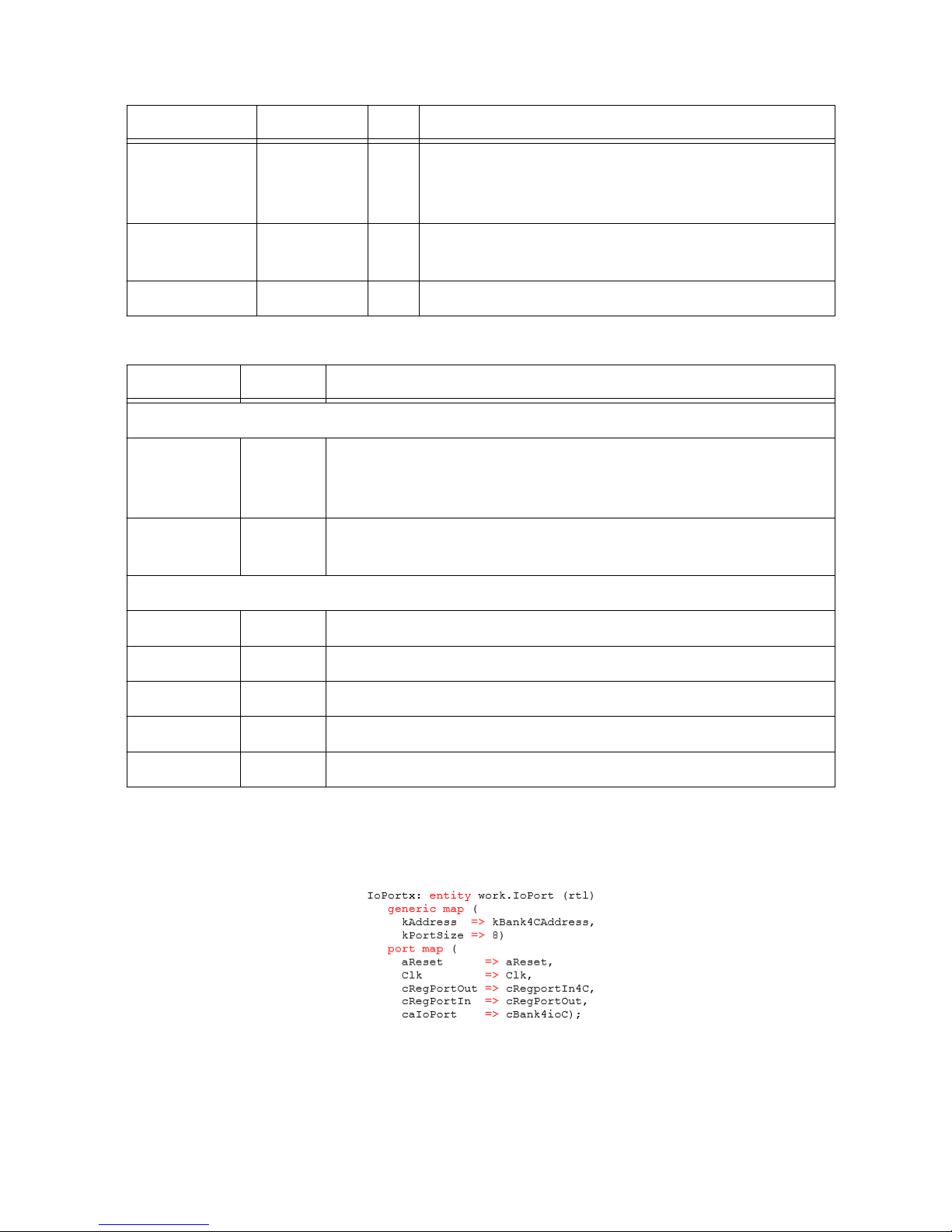
Table 4. Register Descriptions
Register Name Address Type Explanation
Output kAddress R/W The value of this register defines the output state
when the corresponding direction bit is set as output
(1).
Direction kAddress + 1 R/W For each pin of the port, 1 configures the pin as an
output and 0 configures the pin an input.
Input kAddress + 2 R Mirrors the state of the external pin for read.
Table 5. Signal Descriptions
Signal Name Direction Explanation
Generics
kAddress N/A Defines the base address of the block. This address will also
correspond to the Output register. The next two consecutive
addresses are assigned to Direction and Input.
kPortSize N/A Determines the number of I/O implemented. Acceptable values go
from 1 to 64.
Signals
aReset In Board Reset Signal
Clk In Stable clock provided by the CPLD.
caIoPort In/Out Digital input/output.
cRegPortOut Out Signals to the EdBlock Register Port.
cRegPortIn In Signals from the EdBlock Register Port.
I/O Port Instantiation
You can instantiate the I/O Port block in your design as follows:
16 | ni.com | SLSC-12101 User Guide
Page 17
SLSC Interrupt
This entity implements an interrupt block that complies with Section 8.1 of the Switch Load
and Signal Conditioning Design Specifications. It is configurable through generic constants. It
can handle edge-sensitive and level-sensitive signals. The configuration on the sensitivity is
controlled through kSensitivity. The incoming interrupts should be synchronous to Clk.
Table 6. Register Descriptions for the Interrupt Block
Register
Name
Address Type Explanation
Status kRegisterBase R A 1 indicates that an interrupt has occurred. The
interrupt is propagated to IntIn# only if the
corresponding bit has been enabled.
Mask kRegisterBase + 1 R A 1 indicates that the corresponding interrupt is
enabled.
Enable kRegisterBase + 2 Strobe Writing a 1 enables the corresponding interrupt
and turns the corresponding bit in the Mask
Register into 1. Writing a 0 has no effect.
Disable kRegisterBase + 3 Strobe Writing a 1 disables the corresponding interrupt
and turns the corresponding bit in the Mask
Register into a 0. Writing a 0 has no effect.
Ack kRegisterBase + 4 Strobe Writing a 1 to the corresponding bit removes the
interrupt condition. This bit is self-clearing.
Writing a 0 has no effect.
Table 7. Signal Descriptions of the Interrupt Component
Signal Name Direction Explanation
Generics
kRegisterBase N/A Defines the base address of the block. This address will
also correspond to the Status register. The next four
consecutive addresses are assigned to Mask,
InterruptEnable, InterruptDisable, and Ack.
kNumberOfInterrupts N/A Determines the number of interrupts implemented.
Acceptable values range from 1 to 64.
kSensitivity N/A Determines the sensitivity of the corresponding line of
cInterruptsIn. A 0 defines a level sensitive interrupts,
while a 1 defines an edge sensitive.
Signals
aReset In Board reset signal.
SLSC-12101 User Guide | © National Instruments | 17
Page 18

Table 7. Signal Descriptions of the Interrupt Component (Continued)
Signal Name Direction Explanation
Clk In Stable clock provided by the CPLD.
cRdyRst In Ready/Rst signal. The Block follows the reset
requirements defined in Chapter 6 of the Switch Load and
Signal Conditioning Design Specifications. Additionally,
this implementation disables and clears all interrupts
when the module goes to Reset.
cRegPortOut Out Signals to the EdBlock Register Port.
cRegPortIn In Signals from the EdBlock Register Port.
cInterrupt_n Out Interrupt signal of the SLSC interface.
cInterruptsIn In Drive 1 to these signals to generate an interrupt. The
sensitivity of each of these signals is configured by
kSensitivity.
Instantiation of the Interrupt Block
You can instantiate the interrupt block in your design as follows.
LED Implementation
This entity provides an LED controller for 2-pin bicolor LEDs. In this case, the entity has two
green/red dual LEDs. The block allows control of the LEDs and illuminates them green, red,
and yellow either in a solid or blinking pattern. The yellow color is achieved by alternating
between red and green at approximately 300 Hz.
This component has a single register; the address is defined by the kAddress generic.
18 | ni.com | SLSC-12101 User Guide
Page 19

Table 8. Relative Addresses of the Interrupt Block Registers
Register Name Address Type Explanation
LedControl kAddress R/W This register contains two groups of 3 fields. Each group
uses a 4-bit nibble of a byte and each controls each of the
LEDs in the front panel.
Table 9. Bitfield Descriptions of the LedControl Register
Field Name Bit Range Field Size
(bits)
Explanation
ReadyColor 0-1 2 Determines whether the LED is lit and in which
color:
• b'00: Off
• b'01: Red
• b'10: Green
• b'11: Yellow
ReadyMode 2 1 Determines how the LED lights:
• b'0: solid
• b'1: toggles
PowerColor 3-5 2 Determines whether the LED is lit and in which
color:
• b'00: Off
• b'01: Red
• b'02: Green
• b'11: Yellow
PowerMode 6 1 Determines how the LED lights:
• b'0: solid
• b'1: toggles
Table 10. Signal Description of the LED Component
Signal Name Direction Explanation
Generics
kAddress N/A Defines the base address of the block. This address corresponds to
the LedControl register.
Signals
aReset In Board reset signal.
SLSC-12101 User Guide | © National Instruments | 19
Page 20

Table 10. Signal Description of the LED Component (Continued)
Signal Name Direction Explanation
Clk In Stable clock provided by the CPLD. It expects a 40 MHz clock.
cRdyRst In Ready/Rst signal. If RdyRst is low, the state of the LED is Power
solid green and Ready off.
cRegPortOut Out Signals to the EdBlock register port.
cRegPortIn In Signals from the EdBlock register port.
cReadyRed Out Connects to the Ready red anode.
cReadyGreen Out Connects to the Ready green anode,
cPowerRed Out Connects to the Power red anode.
cPowerGreen Out Connects to the Power green anode.
Instantiating the LEDs Component
You can instantiate the LEDs component as follows:
Creating Registers
Read and write registers can easily be implemented using the EdBlock register interface by
invoking the RegisterRead and RegisterWrite functions defined in the PkgEdBlock.vhd file.
These two functions have the following signatures:
Function
Signature
RegisterWrite RegisterWrite(<Register Address (natural)>,
cRegPortOut)
RegisterRead RegisterRead(<Register Address (natural)>,
cRegPortOut)
Both functions will return a Boolean value. This value is true if the command in the incoming
master packet matches the function and if the address in the master packet matches the address
20 | ni.com | SLSC-12101 User Guide
Page 21

of the first argument. The following example shows the implementation of a 64-bit read and
write register on address 0x20.
Instantiating a Readable Register with the RegisterRead
Function
Instantiating a Write Register with the RegisterWrite Function
Other Auxiliary Files
These files contain constants used in the shipping version of the CPLD. You can change these
values or create your own files to better fit your design.
File Name
Notes
PkgRevision.vhd Code version.
PkgSlsc12101Registers.vhd Registers constants.
Programming the CPLD
The J18 header is compatible with Altera's 10-pin plug.
SLSC-12101 User Guide | © National Instruments | 21
Page 22

Figure 10. JTAG Header for CPLD Programming
Table 11. CPLD JTAG Pinout Descriptions
J18 Connector Pin Schematic Name CPLD Bank CPLD Pin Pin Name
1 CPLD_TCK 1 P3 #TCK
2 GND
3 CPLD_TDO 1 M5 #TDO
4 3.3 V
5 CPLD_TMS 1 N4 #TMS
6 NC
7 NC
8 NC
9 CPLD_TDI 1 L6 #TDI
10 GND
Pinouts
Front I/O Connector Pinout
See the following image for the front I/O connector pinout.
22 | ni.com | SLSC-12101 User Guide
Page 23

Figure 11. Front Connector Pinout
PIN 31
PIN 44
PIN 30
PIN 15
PIN 1
PIN 16
Prototyping Area
The front connectors J10 and J11 (labeled J1 and J2 on the front panel) are routed directly to
the prototyping area without any series resistors. The traces have 50 Ω characteristic
impedance and support a maximum of 400 mA.
All signals from the CPLD to the prototyping area are routed with 50 Ω characteristic
impedance traces and have a 33.2 Ω series resistor places near the CPLD.
All connections between XJ2 and the RTI prototyping area are routed with 50 Ω characteristic
impedance without any series resistors.
The connections between XJ3 and the RTI prototyping area with high current traces are
capable of carrying 8 A each. For more information, refer to the SLSC-12101 Specifications,
which can be found on ni.com/manuals.
Hole Marking Codes
Holes in the prototyping area are marked according to their purpose, as shown below.
SLSC-12101 User Guide | © National Instruments | 23
Page 24

Table 12. Marking Codes to Identify the Holes in the Prototyping Area
Unconnected Ground Signal Power
Unconnected holes
do not have any
silkscreen marking.
These holes can be
used for any
connections. An
example of this kind
of hole is M8 of
Bank 1.
Holes connected
to ground are
marked with a
solid white square
(represented in
black in this
document). An
example of this
type of hole is
AD4 of Bank 2.
Holes connected to a trace
have a box around them. The
box can be a rectangle around
adjacent holes connected to
traces. An example of this
type of hole is C18 of Bank 3.
An example of a rectangle
enclosing adjacent holes are
holes AB7 to AB9 of Bank 3.
The rectangles have labels
attached providing an
indication of which signals
these are. For example, C18
of Bank 3 is labeled
CPLD(133) and holes AB7 to
AB9 are labeled
CPLD(134:136).
Holes connected
to power rails
have a circle
around them. An
example of this
hole is A23 of
Bank 4, which is
a hole connected
to the 5 V rail.
These may also
have boxes
around them to
help with
labeling.
24 | ni.com | SLSC-12101 User Guide
Page 25

Bank 1 Prototyping Area
Figure 12. Bank 1 Prototyping Area
Table 13. CPLD Connectivity to Bank 1 Prototyping Area
Bank 1 Lattice
Lattice
Location
Schematic
Name
2
CPLD
Bank
CPLD
Pin
HDL Name Physical Channel
Name
C14 Bank1_IO(19) 1 G3 cBank1ioA(0) Bank1_PortA_DIO0
E13 Bank1_IO(20) 1 G4 cBank1ioA(1) Bank1_PortA_DIO1
E14 Bank1_IO(22) 1 H1 cBank1ioA(2) Bank1_PortA_DIO2
AC13 Bank1_IO(23) 1 H2 cBank1ioA(3) Bank1_PortA_DIO3
AC14 Bank1_IO(24) 1 H3 cBank1ioA(4) Bank1_PortA_DIO4
AE14 Bank1_IO(25) 1 H4 cBank1ioA(5) Bank1_PortA_DIO5
AE13 Bank1_IO(27) 1 J1 cBank1ioA(6) Bank1_PortA_DIO6
2
In the silkscreen, these signals are marked CPLD(Pin Number) for space reasons.
SLSC-12101 User Guide | © National Instruments | 25
Page 26

Table 14. Connector 1 Connectivity to Bank 1 Prototyping Area
Connector J1
J1 Pin Schematic Name
3
Lattice
Coordinate
(Bank 1)
J1 Pin Schematic Name
4
Lattice
Coordinate
(Bank 1)
1 Front1_IO(1) A24 23 Front1_IO(23) D24
2 Front1_IO(2) A23 24 Front1_IO(24) D23
3 Front1_IO(3) A22 25 Front1_IO(25) D22
4 Front1_IO(4) A21 26 Front1_IO(26) D21
5 Front1_IO(5) A20 27 Front1_IO(27) D20
6 Front1_IO(6) A19 28 Front1_IO(28) D19
7 Front1_IO(7) A18 29 GND GND
8 Front1_IO(8) A17 30 Front1_IO(30) D17
9 Front1_IO(9) A16 31 Front1_IO(31) D16
10 Front1_IO(10) A15 32 Front1_IO(32) D15
11 Front1_IO(11) A14 33 Front1_IO(33) D14
12 Front1_IO(12) A13 34 Front1_IO(34) D13
13 Front1_IO(13) A12 35 Front1_IO(35) D12
14 Front1_IO(14) A11 36 Front1_IO(36) D11
15 Front1_IO(15) A10 37 Front1_IO(37) D10
16 Front1_IO(16) A9 38 Front1_IO(38) D9
17 GND GND 39 Front1_IO(39) D8
18 Front1_IO(18) A7 40 Front1_IO(40) D7
19 Front1_IO(19) A6 41 Front1_IO(41) D6
20 Front1_IO(20) A5 42 Front1_IO(42) D5
3
In the silkscreen, these signals are marked IO1(Pin Number) for space reasons.
4
In the silkscreen, these signals are marked IO1(Pin Number) for space reasons.
26 | ni.com | SLSC-12101 User Guide
Page 27

Table 14. Connector 1 Connectivity to Bank 1 Prototyping Area (Continued)
Connector J1
J1 Pin Schematic Name
3
Lattice
Coordinate
(Bank 1)
J1 Pin Schematic Name
4
Lattice
Coordinate
(Bank 1)
21 Front1_IO(21) A4 43 Front1_IO(43) D4
22 Front1_IO(22) A3 44 Front1_IO(44) D3
Table 15. Miscellaneous Signals In Bank 1 Prototyping Area
Miscellaneous Signals
Coordinate Signal Coordinate Signal
A1-D1 3.3 V B2-B24 GND
A25-D15 3.3 V E25-AC25 GND
AD1 3.3 V AD2-AD24 GND
AE1 3.3 V C24 GND
AD25 3.3 V C23 VCC (5 V)
AE25 3.3 V AE16 LAT_CLK2
E1-AC1 GND AE17 LAT_CLK1
3
In the silkscreen, these signals are marked IO1(Pin Number) for space reasons.
4
In the silkscreen, these signals are marked IO1(Pin Number) for space reasons.
SLSC-12101 User Guide | © National Instruments | 27
Page 28

Bank 2 Prototyping Area
Figure 13. Bank 2 Prototyping Area
Table 16. CPLD Connectivity to Bank 2 Prototyping Area
Bank 2 Lattice
Lattice
Location
Schematic Name CPLD
Bank
CPLD
Pin
HDL Name Physical Channel
Name
C19 Bank2_IO(51) 2 A10 cBank2ioA(0) Bank2_PortA_DIO0
C18 Bank2_IO(52) 2 A11 cBank2ioA(1) Bank2_PortA_DIO1
C17 Bank2_IO(53) 2 A12 cBank2ioA(2) Bank2_PortA_DIO2
C16 Bank2_IO(54) 2 A13 cBank2ioA(3) Bank2_PortA_DIO3
C15 Bank2_IO(55) 2 A15 cBank2ioA(4) Bank2_PortA_DIO4
C14 Bank2_IO(56) 2 A2 cBank2ioA(5) Bank2_PortA_DIO5
C13 Bank2_IO(57) 2 A4 cBank2ioA(6) Bank2_PortA_DIO6
C12 Bank2_IO(58) 2 A5 cBank2ioA(7) Bank2_PortA_DIO7
C11 Bank2_IO(59) 2 A6 cBank2ioB(0) Bank2_PortB_DIO0
C10 Bank2_IO(60) 2 A7 cBank2ioB(1) Bank2_PortB_DIO1
C9 Bank2_IO(61) 2 A8 cBank2ioB(2) Bank2_PortB_DIO2
28 | ni.com | SLSC-12101 User Guide
Page 29

Table 16. CPLD Connectivity to Bank 2 Prototyping Area (Continued)
Bank 2 Lattice
Lattice
Location
Schematic Name CPLD
Bank
CPLD
Pin
HDL Name Physical Channel
Name
C8 Bank2_IO(62) 2 A9 cBank2ioB(3) Bank2_PortB_DIO3
E8 Bank2_IO(64) 2 B10 cBank2ioB(4) Bank2_PortB_DIO4
E9 Bank2_IO(65) 2 B11 cBank2ioB(5) Bank2_PortB_DIO5
E10 Bank2_IO(66) 2 B12 cBank2ioB(6) Bank2_PortB_DIO6
E11 Bank2_IO(67) 2 B13 cBank2ioB(7) Bank2_PortB_DIO7
E12 Bank2_IO(68) 2 B14 cBank2ioC(0) Bank2_PortC_DIO0
E13 Bank2_IO(69) 2 B16 cBank2ioC(1) Bank2_PortC_DIO1
E14 Bank2_IO(70) 2 B3 cBank2ioC(2) Bank2_PortC_DIO2
E15 Bank2_IO(71) 2 B4 cBank2ioC(3) Bank2_PortC_DIO3
E16 Bank2_IO(72) 2 B5 cBank2ioC(4) Bank2_PortC_DIO4
E17 Bank2_IO(73) 2 B6 cBank2ioC(5) Bank2_PortC_DIO5
E18 Bank2_IO(74) 2 B7 cBank2ioC(6) Bank2_PortC_DIO6
E19 Bank2_IO(75) 2 B8 cBank2ioC(7) Bank2_PortC_DIO7
AC8 Bank2_IO(78) 2 C11 cBank2ioD(0) Bank2_PortD_DIO0
AC9 Bank2_IO(79) 2 C12 cBank2ioD(1) Bank2_PortD_DIO1
AC10 Bank2_IO(80) 2 C13 cBank2ioD(2) Bank2_PortD_DIO2
AC11 Bank2_IO(81) 2 C4 cBank2ioD(3) Bank2_PortD_DIO3
AC12 Bank2_IO(82) 2 C5 cBank2ioD(4) Bank2_PortD_DIO4
AC13 Bank2_IO(83) 2 C6 cBank2ioD(5) Bank2_PortD_DIO5
AC14 Bank2_IO(84) 2 C7 cBank2ioD(6) Bank2_PortD_DIO6
AC15 Bank2_IO(85) 2 C8 cBank2ioD(7) Bank2_PortD_DIO7
AC16 Bank2_IO(86) 2 C9 cBank2ioE(0) Bank2_PortE_DIO0
AC17 Bank2_IO(87) 2 D10 cBank2ioE(1) Bank2_PortE_DIO1
AC18 Bank2_IO(88) 2 D11 cBank2ioE(2) Bank2_PortE_DIO2
AC19 Bank2_IO(89) 2 D12 cBank2ioE(3) Bank2_PortE_DIO3
AE19 Bank2_IO(90) 2 D4 cBank2ioE(4) Bank2_PortE_DIO4
SLSC-12101 User Guide | © National Instruments | 29
Page 30

Table 16. CPLD Connectivity to Bank 2 Prototyping Area (Continued)
Bank 2 Lattice
Lattice
Location
Schematic Name CPLD
Bank
CPLD
Pin
HDL Name Physical Channel
Name
AE18 Bank2_IO(91) 2 D5 cBank2ioE(5) Bank2_PortE_DIO5
AE17 Bank2_IO(92) 2 D6 cBank2ioE(6) Bank2_PortE_DIO6
AE16 Bank2_IO(93) 2 D7 cBank2ioE(7) Bank2_PortE_DIO7
AE15 Bank2_IO(94) 2 D8 cBank2ioF(0) Bank2_PortF_DIO0
AE14 Bank2_IO(95) 2 D9 cBank2ioE(1) Bank2_PortF_DIO0
AE13 Bank2_IO(96) 2 E10 cBank2ioE(2) Bank2_PortF_DIO0
AE12 Bank2_IO(97) 2 E11 cBank2ioE(3) Bank2_PortF_DIO0
AE11 Bank2_IO(98) 2 E6 cBank2ioE(4) Bank2_PortF_DIO0
AE10 Bank2_IO(99) 2 E7 cBank2ioE(5) Bank2_PortF_DIO0
AE9 Bank2_IO(100) 2 E8 cBank2ioE(6) Bank2_PortF_DIO0
AE8 Bank2_IO(101) 2 E9 cBank2ioE(7) Bank2_PortF_DIO0
Table 17. Connector 2 Connectivity to Bank 2 Prototyping Area
Connector J2
J2 Pin Schematic Name
5
Lattice
Coordinate
(Bank 2)
J2 Pin Schematic Name
6
Lattice
Coordinate
(Bank 2)
1 Front2_IO(1) A24 23 Front2_IO(23) D24
2 Front2_IO(2) A23 24 Front2_IO(24) D23
3 Front2_IO(3) A22 25 Front2_IO(25) D22
4 Front2_IO(4) A21 26 Front2_IO(26) D21
5 Front2_IO(5) A20 27 Front2_IO(27) D20
6 Front2_IO(6) A19 28 Front2_IO(28) D19
7 Front2_IO(7) A18 29 GND GND
8 Front2_IO(8) A17 30 Front2_IO(30) D17
5
In the silkscreen, these signals are marked IO2(Pin Number) for space reasons
6
In the silkscreen, these signals are marked IO2(Pin Number) for space reasons
30 | ni.com | SLSC-12101 User Guide
Page 31

Table 17. Connector 2 Connectivity to Bank 2 Prototyping Area (Continued)
Connector J2
J2 Pin Schematic Name
5
Lattice
Coordinate
(Bank 2)
J2 Pin Schematic Name
6
Lattice
Coordinate
(Bank 2)
9 Front2_IO(9) A16 31 Front2_IO(31) D16
10 Front2_IO(10) A15 32 Front2_IO(32) D15
11 Front2_IO(11) A14 33 Front2_IO(33) D14
12 Front2_IO(12) A13 34 Front2_IO(34) D13
13 Front2_IO(13) A12 35 Front2_IO(35) D12
14 Front2_IO(14) A11 36 Front2_IO(36) D11
15 Front2_IO(15) A10 37 Front2_IO(37) D10
16 Front2_IO(16) A9 38 Front2_IO(38) D9
17 GND GND 39 Front2_IO(39) D8
18 Front2_IO(18) A7 40 Front2_IO(40) D7
19 Front2_IO(19) A6 41 Front2_IO(41) D6
20 Front2_IO(20) A5 42 Front2_IO(42) D5
21 Front2_IO(21) A4 43 Front2_IO(43) D4
22 Front2_IO(22) A3 44 Front2_IO(44) D3
Table 18. Miscellaneous Signals in Bank 2 Prototyping Area
Miscellaneous Signals
Coordinate Signal Coordinate Signal
A1-D1 BANK2_VCC E1-AC1 GND
A25-D15 BANK2_VCC B2-B24 GND
AD1 BANK2_VCC E25-AC25 GND
AE1 BANK2_VCC AD2-AD24 GND
AD25 BANK2_VCC C24 GND
AE25 BANK2_VCC C23 VCC (5 V)
5
In the silkscreen, these signals are marked IO2(Pin Number) for space reasons
6
In the silkscreen, these signals are marked IO2(Pin Number) for space reasons
SLSC-12101 User Guide | © National Instruments | 31
Page 32

Bank 3 Prototyping Area
Figure 14. Bank 3 Prototyping Area
Table 19. CPLD Connectivity to Bank 3 Prototyping Area
Bank 3 Lattice
Lattice
Location
Schematic
Name
7
CPLD
Bank
CPLD
Pin
HDL Name Physical Channel
Name
A18 Bank3_IO(104) 3 C14 cBank3ioA(0) Bank3_PortA_DIO0
A17 Bank3_IO(105) 3 C15 cBank3ioA(1) Bank3_PortA_DIO1
A16 Bank3_IO(106) 3 D13 cBank3ioA(2) Bank3_PortA_DIO2
A15 Bank3_IO(107) 3 D14 cBank3ioA(3) Bank3_PortA_DIO3
A14 Bank3_IO(108) 3 D15 cBank3ioA(4) Bank3_PortA_DIO4
A13 Bank3_IO(109) 3 D16 cBank3ioA(5) Bank3_PortA_DIO5
A12 Bank3_IO(110) 3 E12 cBank3ioA(6) Bank3_PortA_DIO6
A11 Bank3_IO(111) 3 E13 cBank3ioA(7) Bank3_PortA_DIO7
A10 Bank3_IO(112) 3 E14 cBank3ioB(0) Bank3_PortB_DIO0
A9 Bank3_IO(113) 3 E15 cBank3ioB(1) Bank3_PortB_DIO1
7
In the silkscreen, these signals are marked as CPLD(Pin Number) for space reasons.
32 | ni.com | SLSC-12101 User Guide
Page 33

Table 19. CPLD Connectivity to Bank 3 Prototyping Area (Continued)
Bank 3 Lattice
Lattice
Location
Schematic
Name
7
CPLD
Bank
CPLD
Pin
HDL Name Physical Channel
Name
A8 Bank3_IO(114) 3 E16 cBank3ioB(2) Bank3_PortB_DIO2
C7 Bank3_IO(115) 3 F11 cBank3ioB(3) Bank3_PortB_DIO3
C8 Bank3_IO(116) 3 F12 cBank3ioB(4) Bank3_PortB_DIO4
C9 Bank3_IO(117) 3 F13 cBank3ioB(5) Bank3_PortB_DIO5
C10 Bank3_IO(118) 3 F14 cBank3ioB(6) Bank3_PortB_DIO6
C11 Bank3_IO(119) 3 F15 cBank3ioB(7) Bank3_PortB_DIO7
C12 Bank3_IO(120) 3 F16 cBank3ioC(0) Bank3_PortC_DIO0
C13 Bank3_IO(122) 3 G12 cBank3ioC(1) Bank3_PortC_DIO1
C14 Bank3_IO(123) 3 G13 cBank3ioC(2) Bank3_PortC_DIO2
C15 Bank3_IO(124) 3 G14 cBank3ioC(3) Bank3_PortC_DIO3
C16 Bank3_IO(125) 3 G15 cBank3ioC(4) Bank3_PortC_DIO4
C17 Bank3_IO(126) 3 G16 cBank3ioC(5) Bank3_PortC_DIO5
C18 Bank3_IO(133) 3 J13 cBank3ioC(6) Bank3_PortC_DIO6
AB7 Bank3_IO(134) 3 J14 cBank3ioD(0) Bank3_PortD_DIO0
AB8 Bank3_IO(135) 3 J15 cBank3ioD(1) Bank3_PortD_DIO1
AB9 Bank3_IO(136) 3 J16 cBank3ioD(2) Bank3_PortD_DIO2
AB10 Bank3_IO(138) 3 K12 cBank3ioD(3) Bank3_PortD_DIO3
AB11 Bank3_IO(139) 3 K13 cBank3ioD(4) Bank3_PortD_DIO4
AB12 Bank3_IO(140) 3 K14 cBank3ioD(5) Bank3_PortD_DIO5
AB13 Bank3_IO(141) 3 K15 cBank3ioD(6) Bank3_PortD_DIO6
AB14 Bank3_IO(142) 3 K16 cBank3ioD(7) Bank3_PortD_DIO7
AB15 Bank3_IO(143) 3 L11 cBank3ioE(0) Bank3_PortE_DIO0
AB16 Bank3_IO(144) 3 L12 cBank3ioE(1) Bank3_PortE_DIO1
AB17 Bank3_IO(145) 3 L13 cBank3ioE(2) Bank3_PortE_DIO2
AB18 Bank3_IO(146) 3 L14 cBank3ioE(3) Bank3_PortE_DIO3
7
In the silkscreen, these signals are marked as CPLD(Pin Number) for space reasons.
SLSC-12101 User Guide | © National Instruments | 33
Page 34

Table 19. CPLD Connectivity to Bank 3 Prototyping Area (Continued)
Bank 3 Lattice
Lattice
Location
Schematic
Name
7
CPLD
Bank
CPLD
Pin
HDL Name Physical Channel
Name
AD19 Bank3_IO(147) 3 L15 cBank3ioE(4) Bank3_PortE_DIO4
AD18 Bank3_IO(148) 3 L16 cBank3ioE(5) Bank3_PortE_DIO5
AD17 Bank3_IO(149) 3 M13 cBank3ioE(6) Bank3_PortE_DIO6
AD16 Bank3_IO(150) 3 M14 cBank3ioE(7) Bank3_PortE_DIO7
AD15 Bank3_IO(151) 3 M15 cBank3ioF(0) Bank3_PortF_DIO0
AD14 Bank3_IO(152) 3 M16 cBank3ioF(1) Bank3_PortF_DIO1
AD13 Bank3_IO(153) 3 N13 cBank3ioF(2) Bank3_PortF_DIO2
AD12 Bank3_IO(154) 3 N14 cBank3ioF(3) Bank3_PortF_DIO3
AD11 Bank3_IO(155) 3 N15 cBank3ioF(4) Bank3_PortF_DIO4
AD10 Bank3_IO(156) 3 N16 cBank3ioF(5) Bank3_PortF_DIO5
AD9 Bank3_IO(157 3 P14 cBank3ioF(6) Bank3_PortF_DIO6
AD8 Bank3_IO(158) 3 P15 cBank3ioF(7) Bank3_PortF_DIO7
Table 20. Miscellaneous Signals in Bank 3 Prototyping Area
Miscellaneous Signals
Coordinate Signal Coordinate Signal
A1 BANK3_VCC C1-AB1 GND
B1 BANK3_VCC B2-B24 GND
A25 BANK3_VCC C25-AB25 GND
B25 BANK3_VCC AC2-AC24 GND
AC1 BANK3_VCC A24 GND
AD1 BANK3_VCC A23 VCC (5 V)
AC25 BANK3_VCC AD21 LAT_CLK4
AD25 BANK3_VCC AD22 LAT_CLK3
7
In the silkscreen, these signals are marked as CPLD(Pin Number) for space reasons.
34 | ni.com | SLSC-12101 User Guide
Page 35

Bank 4 Prototyping Area
Figure 15. Bank 4 Prototyping Area
Table 21. CPLD Connectivity to Bank 4 Prototyping Area
Bank 4 Lattice
Lattice
Location
Schematic
Name
8
CPLD
Bank
CPLD
Pin
HDL Name Physical Channel
Name
A17 Bank4_IO(161) 4 M10 cBank4ioA(0) Bank4_PortA_DIO0
A16 Bank4_IO(162) 4 M11 cBank4ioA(1) Bank4_PortA_DIO1
A15 Bank4_IO(163) 4 M12 cBank4ioA(2) Bank4_PortA_DIO2
A14 Bank4_IO(164) 4 M6 cBank4ioA(3) Bank4_PortA_DIO3
A13 Bank4_IO(165) 4 M7 cBank4ioA(4) Bank4_PortA_DIO4
A12 Bank4_IO(168) 4 N10 cBank4ioA(5) Bank4_PortA_DIO5
A11 Bank4_IO(169) 4 N11 cBank4ioA(6) Bank4_PortA_DIO6
A10 Bank4_IO(170) 4 N12 cBank4ioA(7) Bank4_PortA_DIO7
C10 Bank4_IO(171) 4 N5 cBank4ioB(0) Bank4_PortB_DIO0
C11 Bank4_IO(188) 4 R11 cBank4ioB(1) Bank4_PortB_DIO1
8
In the silkscreen, these signals are marked as CPLD(Pin Number) for space reasons.
SLSC-12101 User Guide | © National Instruments | 35
Page 36

Table 21. CPLD Connectivity to Bank 4 Prototyping Area (Continued)
Bank 4 Lattice
Lattice
Location
Schematic
Name
8
CPLD
Bank
CPLD
Pin
HDL Name Physical Channel
Name
C12 Bank4_IO(189) 4 R12 cBank4ioB(2) Bank4_PortB_DIO2
C13 Bank4_IO(190) 4 R13 cBank4ioB(3) Bank4_PortB_DIO3
C14 Bank4_IO(191) 4 R14 cBank4ioB(4) Bank4_PortB_DIO4
C15 Bank4_IO(192) 4 R16 cBank4ioB(5) Bank4_PortB_DIO5
C16 Bank4_IO(193) 4 R3 cBank4ioB(6) Bank4_PortB_DIO6
C17 Bank4_IO(194) 4 R4 cBank4ioB(7) Bank4_PortB_DIO7
AB10 Bank4_IO(195) 4 R5 cBank4ioC(0) Bank4_PortC_DIO0
AB11 Bank4_IO(196) 4 R6 cBank4ioC(1) Bank4_PortC_DIO1
AB12 Bank4_IO(197) 4 R7 cBank4ioC(2) Bank4_PortC_DIO2
AB13 Bank4_IO(198) 4 R8 cBank4ioC(3) Bank4_PortC_DIO3
AB14 Bank4_IO(199) 4 R9 cBank4ioC(4) Bank4_PortC_DIO4
AB15 Bank4_IO(200) 4 T10 cBank4ioC(5) Bank4_PortC_DIO5
AB16 Bank4_IO(201) 4 T11 cBank4ioC(6) Bank4_PortC_DIO6
AB17 Bank4_IO(202) 4 T12 cBank4ioC(7) Bank4_PortC_DIO7
AD17 Bank4_IO(203) 4 T13 cBank4ioD(0) Bank4_PortD_DIO0
AD16 Bank4_IO(204) 4 T15 cBank4ioD(1) Bank4_PortD_DIO1
AD15 Bank4_IO(205) 4 T2 cBank4ioD(2) Bank4_PortD_DIO2
AD14 Bank4_IO(206) 4 T4 cBank4ioD(3) Bank4_PortD_DIO3
AD13 Bank4_IO(207) 4 T5 cBank4ioD(4) Bank4_PortD_DIO4
AD12 Bank4_IO(209) 4 T7 cBank4ioD(5) Bank4_PortD_DIO5
AD11 Bank4_IO(210) 4 T8 cBank4ioD(6) Bank4_PortD_DIO6
AD10 Bank4_IO(211) 4 T9 cBank4ioD(7) Bank4_PortD_DIO7
8
In the silkscreen, these signals are marked as CPLD(Pin Number) for space reasons.
36 | ni.com | SLSC-12101 User Guide
Page 37

Table 22. Miscellaneous Signals in Bank 4 Prototyping Area
Miscellaneous Signals
Coordinate Signal Coordinate Signal
A1 BANK4_VCC AD25 BANK4_VCC
B1 BANK4_VCC C1-AB1 GND
A25 BANK4_VCC B2-B24 GND
B25 BANK4_VCC C25-AB25 GND
AC1 BANK4_VCC AC2-AC24 GND
AD1 BANK4_VCC A24 GND
AC25 BANK4_VCC A23 VCC (5 V)
RTI Prototyping Area
Figure 16. RTI Prototyping Area
SLSC-12101 User Guide | © National Instruments | 37
Page 38

Table 23. Connectivity of XJ2 Connector to RTI Prototyping Area
Connector XJ2
XJ2
pin
Lattice
Coordinate
(RTI)
XJ2
pin
Lattice
Coordinate
(RTI)
XJ2
pin
Lattice
Coordinate
(RTI)
XJ2
pin
Lattice
Coordinate
(RTI)
XJ2
pin
Lattice
Coordinate
(RTI)
A1 I10 B1 G10 C1 E10 D1 C10 E1 B10
A2 I11 B2 G11 C2 E11 D2 C11 E2 B11
A3 GND B3 GND C3 GND D3 GND E3 GND
A4 I12 B4 G12 C4 E12 D4 C12 E4 B12
A5 I13 B5 G13 C5 E13 D5 C13 E5 B13
A6 GND B6 GND C6 GND D6 GND E6 GND
A7 I14 B7 G14 C7 E14 D7 C14 E7 B14
A8 I15 B8 G15 C8 E15 D8 C15 E8 B15
A9 GND B9 GND C9 GND D9 GND E9 GND
A10 I16 B10 G16 C10 E16 D10 C16 E10 B16
A11 I17 B11 G17 C11 E17 D11 C17 E11 B17
A15 I18 B15 G18 C15 E18 D15 C18 E15 B18
A16 I19 B16 G19 C16 E19 D16 C19 E16 B19
A17 GND B17 GND C17 GND D17 GND E17 GND
A18 I20 B18 G20 C18 E20 D18 C20 E18 B20
A19 I21 B19 G21 C19 E21 D19 C21 E19 B21
A20 GND B20 GND C20 GND D20 GND E20 GND
A21 I22 B21 G22 C21 E22 D21 C22 E21 B22
A22 I23 B22 G23 C22 E23 D22 C23 E22 B23
A23 GND B23 GND C23 GND D23 GND E23 GND
A24 I24 B24 G24 C24 E24 D24 C24 E24 B24
A25 I25 B25 G25 C25 E25 D25 C25 E25 B25
38 | ni.com | SLSC-12101 User Guide
Page 39

Table 24. Connectivity of XJ3 Connector to RTI Prototyping Area
Connector XJ3
XJ3 Pin Lattice Coordinates (RTI)
A I(3-6)
B H(3-6)
C G(3-6)
D F(3-6)
E E(3-6)
F D(3-6)
G C(3-6)
H B(3-6)
Table 25. RTI Miscellaneous Signals
Miscellaneous Signals
Coordinate Signal Coordinate Signal
B1-I1 GND J3-J6 24 V
A2 GND A7-A26 GND
B2-C2 3.3 V J7-J26 GND
D2-E2 Bank 2 VCC D26-E26 Bank 2 VCC
F2-G2 Bank 3 VCC F26-G26 Bank 3 VCC
H2-I2 Bank 4 VCC H26-I26 Bank 4 VCC
A3-A6 24 V B27-I27 GND
SLSC-12101 User Guide | © National Instruments | 39
Page 40

CPLD Pins
Table 26. Miscellaneous Connections to the CPLD
Miscellaneous Pins
Schematic Name CPLD Bank CPLD Pin Pin Name Notes
Bank2_IO(77) 2 C10 aTFM_Lattice
Bank2_IO(76) 2 B9 aTTM_Lattice
Bank2_IO(63) 2 B1 unused
CPLD_CLK1 1 H5 Clk System clock for the design.
LED_Red_0 1 L1 cPowerGreen LED signal.
LED_Green_0 1 L3 cPowerRed LED signal.
LED_Red_1 1 L2 cReadyGreen LED signal.
LED_Green_1 1 L4 cReadyRed LED signal.
CPLDESET# 1 K4 aReset_n Module Reset.
Table 27. Rotary Switch Connectivity to the CPLD
Rotary Switch
SW1 pin Schematic Name CPLD Bank CPLD Pin HDL Name Physical Channel
Name
1 Switch(0) 3 H16 aSwitch(0) NI.RotarySwitch
2 Switch(1) 3 H15 aSwitch(1) NI.RotarySwitch
4 Switch(2) 3 H14 aSwitch(2) NI.RotarySwitch
8 Switch(3) 3 H13 aSwitch(3) NI.RotarySwitch
C Bank3_VCC
Table 28. SI 5356 Clock Generator Connectivity to the CPLD
SI5356 Clock Generator Interface
SI5356 pin Schematic Name CPLD Bank CPLD Pin HDL Name
8 CLK_INT 1 F5 unused
18 CPLD_CLK2 1 J5 unused
14 CPLD_CLK3 3 H12 unused
40 | ni.com | SLSC-12101 User Guide
Page 41

Table 28. SI 5356 Clock Generator Connectivity to the CPLD (Continued)
SI5356 Clock Generator Interface
SI5356 pin Schematic Name CPLD Bank CPLD Pin HDL Name
10 CPLD_CLK4 3 J12 unused
12 SCL_HDR 1 F6 unused
19 SDA_HDR 1 G1 unused
5 SSC_DIS 1 K5 unused
Table 29. Temperature Sensors Connectivity to the CPLD
Temperature Sensors
Pin Number on Sensor
Sensor1Sensor2Sensor3Sensor
4
Schematic
Name
CPLD
Bank
CPLD
Pin
HDL Name
1 1 SPI0_CLK 1 C2 aSpi0Clk
2 2 SPI0_MISO 1 C3 aSpi0Miso
3 3 SPI0_MOSI 1 D1 aSpi0Mosi
4 SPI0_CS#(0) 1 D2 aSpi0Ss(0)
4 SPI0_CS#(1) 1 D3 aSpi0Ss(1)
6 6 L0_CT 1 F1 aL0Ct
5 5 L0_INT 1 F2 aL0Int
1 1 SPI1_CLK 1 E1 aSpi1Clk
2 2 SPI1_MISO 1 E2 aSpi1Miso
3 3 SPI1_MOSI 1 E3 aSpi1Mosi
4 SPI1_CS#(0) 1 E4 aSpi1Ss(0)
4 SPI1_CS#(1) 1 E5 aSpi1Ss(1)
6 6 L1_CT 1 F3 aL1Ct
5 5 L1_INT 1 F4 aL1Int
Deploying the SLSC-12101 as a Final Product
If you decide to use a modified SLSC-12101 as a final product, it is your responsibility to
make sure that the product is modified and used in such a way that complies with local rules,
SLSC-12101 User Guide | © National Instruments | 41
Page 42

regulations, and best practices. Additionally, the modules must comply with the requirements
specified in this section.
Module Design Specification Compliance
Use, design, and distribution of this module must comply with the Switch Load and Signal
Conditioning Module Design Specifications, as well as the license agreement included in the
SLSC Module Development Kit.
Regulatory Compliance and Markings
All compliance testing and certifications for the SLSC-12101 apply only to the unmodified
module. Any modification to the module requires the removal of regulatory markings.
Cosmetic Alterations
The module should not be deployed as a final product without cosmetic modification. Be sure
to make the following changes:
• Remove the National Instruments label on the ejector handle. This may be replaced with
another label, such as one with the corporate logo of the module developer.
• On the front panel, cover or remove the model name and description ("SLSC-12101
Prototyping Module").
• Customize LED and connector labeling as needed.
• Add the new model name and pertinent information. A custom overlay may be used for
this purpose. See the Switch Load and Signal Conditioning Module Design Specifications
for more details.
• Update the blank SLSC Rear I/O Compatibility Glyph on the SLSC-12101 front panel
with the proper alphanumeric code to reflect the final module rear I/O implementation.
See the Switch Load and Signal Conditioning Module Design Specifications for more
details.
SLSC-12101 Bill of Materials
Table 30. Bill of Materials for the SLSC-12101
Reference
Designator
Description Qty Manufacturer Part Number
06 JUMPER, 2 X 1,
0.100 IN (2.54 MM)
PITCH, BLUE,
GOLD-PLATED
3 SAMTEC SNT-100-BL-G
C001 CAP, SM, 75 PF, 50
V, 1%, COG, CER,
0402, H= .022 IN
1 KEMET C0402C750F5GACTU
42 | ni.com | SLSC-12101 User Guide
Page 43

Table 30. Bill of Materials for the SLSC-12101 (Continued)
Reference
Designator
Description Qty Manufacturer Part Number
C002, C005, C008 CAP, SM, 820 PF,
50 V, 5%, COG,
0402, H= .029 IN
3 MURATA GRM1555C1H821JA01D
C003, C004, C006,
C009
CAP, SM, 1 UF, 16
V, 10%, X7R, 0603,
H= .035 IN
4 KEMET C0603C105K4RACTU
C007 CAP, SM, 220 PF,
50 V, 5%, COG,
CER, 0603, H= .033
IN
1 MURATA GRM1885C1H221JA01D
C011 CAP, SM, 0.1 UF,
50 V, 10%, X7R,
CER, 0603, H= .039
IN
1 VENKEL C0603X7R500-104KNP
C014, C015, C020,
C023
CAP, SM, 10 UF, 50
V, 20%, X7S, 1210,
H= .106 IN
4 TAIYO YUDEN UMK325C7106MM-T
C016, C021 CAP, SM, 10 UF, 25
V, 10%, X7R, 1210,
H= .083 IN
2 MURATA GRM32DR71E106KA12L
C017, C026, C031,
C033, C035, C036,
C038, C042, C043,
C048, C050, C051,
C053
CAP, SM, 0.1 UF,
16 V, 10%, X7R,
CER, 0402, H= .025
IN
13 AVX 0402YC104KAT2A
C024 CAP, SM, 330 UF,
6.3 V, 20%,
POLYMER
TANTALUM,
A_RMS =3.2 AMP
@20 C, 7343, H= .
122 IN
1 VENKEL TA6R3PCJ337MDR0015
C027, C030, C056,
C059
CAP, SM, 0.01 UF,
16 V, 5%,
CERAMIC, COG,
0805, H= .055 IN
4 VENKEL C0805C0G500-103JNP
SLSC-12101 User Guide | © National Instruments | 43
Page 44

Table 30. Bill of Materials for the SLSC-12101 (Continued)
Reference
Designator
Description Qty Manufacturer Part Number
C028, C029, C057,
C058
CAP, SM, 2700 PF,
50V, 5%, COG,
CER, 0603, H =.039
IN
4 MURATA GRM1885C1H272JA01D
C032, C039, C040,
C041, C044, C045,
C047, C054
CAP, SM, 100 UF,
6.3 V, 20%, CER,
X5R, 1210, H= .106
IN
8 VENKEL C1210X5R6R3-107MNU
C034, C037, C049,
C052
CAP, SM, 22 UF, 16
V, 10%, CER, X5R,
1210, H= .125 IN
4 MURATA GRM32ER61C226KE20L
C062, C064, C066,
C067, C072, C073,
C074, C081, C082,
C083, C084, C085,
C086, C087, C088,
C089, C091, C094,
C095, C096, C097,
C098, C099, C100,
C101, C102, C103,
C104, C105
CAP, SM, 0.1 UF,
16 V, 10%, X7R,
CER, 0402, H= .025
IN
29 AVX 0402YC104KAT2A
C065 CAP, SM, 820 PF,
50 V, 5%, COG,
0402, H= .029 IN
1 MURATA GRM1555C1H821JA01D
C068, C069, C070,
C071
CAP, SM, 680 PF,
5%, 50 V, COG,
0603, H= .034 IN
4 AVX 06035A681JAT2A
CR001, CR002 DIODE, SM,
SCHOTTKY,
MSS1P6, 60 V, 2PIN MICROSMP,
H= .029 IN
2 VISHAY MSS1P6-M3/89A
CR003, CR004 DIODE, SM,
BAT54,
SCHOTTKY,
DUAL, SOT-323,
H= .039 IN
2 NXP BAT54SW,115
44 | ni.com | SLSC-12101 User Guide
Page 45

Table 30. Bill of Materials for the SLSC-12101 (Continued)
Reference
Designator
Description Qty Manufacturer Part Number
CR005 DIODE,SM,
ZENER, 3W, 6.2 V,
403 A
1 ON
SEMICONDUCTOR
1SMB5920BT3G
DS001 LED, TH, DUAL-
LEVEL,
INDICATOR RED/
GREEN, H= .395 IN
1 DIALIGHT 5530711F
F001 FUSE, SM,
NANO2, 3.5 A, 125
V, W/OMNI-BLOK
FUSEHOLDER,
FAST, H= .150 IN
1 LITTELFUSE 015403.5DRT
J010, J011 CONN, RCPT, HDR
D SUB, 44 POS,
PWB MT
2 TE
CONNECTIVITY
5748482-5
J017 CONN, MICTOR
38, RCPT, SM W /
THRU HOLE
GROUND BUS,
VERT, KEYED,
H= .242 IN
1 TE
CONNECTIVITY
5767171-1
J018 CONN, SM, HDR,
2X5.100, POST
H= .380 IN
1 SAMTEC TSM-105-01-TM-DV-P-
TR
L001 INDUCTOR, SM,
10 UH, 20%, 7.5 A,
H=.158 IN
1 VISHAY-DALE IHLP4040DZER100M11
L002, L003, L004,
L005
INDUCTOR, SM,
LOW PROFILE
HIGH CURRENT,
3.3 UH, 20%, 6 A,
H= .118 IN
4 VISHAY-DALE IHLP2525CZER3R3M01
Q001 TRANSISTOR, SM,
FDG6335N, DUAL
N-CHANNEL FET,
SC-70-6, H= .043
IN
1 FAIRCHILD FDG6335N
SLSC-12101 User Guide | © National Instruments | 45
Page 46

Table 30. Bill of Materials for the SLSC-12101 (Continued)
Reference
Designator
Description Qty Manufacturer Part Number
Q002, Q003 TRANSISTOR, SM,
MOSFET,
BSC097N06NS, NCHANNEL 60 V
OPTIMOS,
POWER, PGTDSON-8, H= .043
IN
2 INFINEON BSC097N06NSATMA1
R001, R006, R007,
R008, R049, R061,
R062, R167, R171,
R172, R173
RES, SM, 10K, 1/16
W, .5%,
THINFILM, 25
PPM, 0402, H= .016
IN
11 VENKEL TFCR0402-16W-
E-1002DT
R002 RES, SM, 45.3 K,
1/16 W, 0.5%, +/-25
PPM, THIN FILM,
0402, H= .016 IN
1 THIN FILM
TECHNOLOGY
RR0510P4532D-C
R003, R010 RES, SM, 10.7 K,
1/16 W, 0.5%, 25
PPM, THIN FILM,
0402, H= .016 IN
2 IRC PCF-W0402LF-03-1072-
D-P-LT
R004, R013 RES, SM, 1 K, 1/16
W, 50 V, 1%,
THICK FILM, 0402,
H= .014 IN
2 VISHAY-DALE CRCW04021K00FKED
R005 RES, SM, 3.32, 1/4
W, 1%, 200 PPM,
THICK FILM, 1206,
H= .028 IN
1 VENKEL CR1206-4W-3R32FT
R009 RES, SM, 75 K,
1/16 W, 50 V, 1%,
THICK FILM, 0402,
H= .016 IN
1 VISHAY-DALE CRCW040275K0FKED
R011 RES, SM, 0, 1/10 W,
5%, 200 PPM,
THICK FILM, 0603,
H= .0217 IN
1 VENKEL CR0603-10W-000SNT
46 | ni.com | SLSC-12101 User Guide
Page 47

Table 30. Bill of Materials for the SLSC-12101 (Continued)
Reference
Designator
Description Qty Manufacturer Part Number
R012, R014 RES, SM, 10, 1/10
W, 50 V, 1%,
THICK FILM, 0603,
H= .020 IN
2 VENKEL CR0603-10W-10R0FT
R015 RES, SM, 0.015, 1
W, 1%, THIN
FILM, 0815, H= .
022 IN
1 THIN FILM
TECHNOLOGY
RL3720WTR015F-C
R016, R168 RES, SM, 0, 1/4 W,
5%, THICK FILM,
1206
2 YAGEO /
PHYCOMP
RC1206JR-070RL
SLSC-12101 User Guide | © National Instruments | 47
Page 48

Table 30. Bill of Materials for the SLSC-12101 (Continued)
Reference
Designator
Description Qty Manufacturer Part Number
R018, R019, R026,
R028, R037, R039,
R041, R042, R043,
R044, R045, R046,
R047, R048, R051,
R052, R053, R054,
R055, R056, R057,
R058, R059, R060,
R067, R068, R069,
R070, R071, R072,
R073, R074, R075,
R076, R077, R078,
R084, R085, R089,
R090, R091, R092,
R093, R094, R095,
R096, R097, R098,
R099, R100, R101,
R102, R103, R104,
R105, R106, R111,
R112, R113, R114,
R115, R116, R117,
R118, R119, R120,
R121, R122, R123,
R124, R125, R126,
R127, R128, R129,
R130, R131, R132,
R137, R138, R139,
R140, R141, R142,
R143, R144, R147,
R148, R149, R150,
R151, R152, R153,
R154, R156, R157,
R158, R159, R160,
R161, R162, R164,
R165, R170, R174
RES, SM, 33.2 ,1/16
W, 50 V, 1%,
THICK FILM, 0402,
H= .016 IN
105 VISHAY-DALE CRCW040233R2FKEDC
R020, R145, R146 RES, SM, 47 K,
1/16 W, 0.5%, 25
PPM, THIN FILM,
0402, H= .014 IN
3 VENKEL TFCR0402-16W-
E-4702DT
48 | ni.com | SLSC-12101 User Guide
Page 49

Table 30. Bill of Materials for the SLSC-12101 (Continued)
Reference
Designator
Description Qty Manufacturer Part Number
R021, R134, R136 RES, SM, 27 K
OHM, 1/16 W, 1%,
THICK FILM, 0402,
H= .016 IN
3 VISHAY-DALE CRCW040227K0FKED
R022, R133, R135 RES, SM, 15 K,
1/16 W, .5%, THIN
FILM, 25 PPM,
0402, H= .016 IN
3 VENKEL TFCR0402-16W-
E-1502DT
R023, R108, R110 RES, SM .8.2 K
OHM, 1/16 W, 1%,
50 V, 100 PPM,
THICK FILM, 0402,
H= .016 IN
3 VISHAY-DALE CRCW04028K20FKED
R024, R107, R109 RES, SM, 4.7 K
OHM, 1/16 W, 1%,
THICK FILM, 0402,
H= .016 IN
3 KOA RK73H1ETTP4701F
R025, R029, R166 RES, SM, 1 K, 1/16
W, .5%, THIN
FILM, 25 PPM,
0402 ,H= .016 IN
3 THINFILM RR0510P102D-C
R030, R033, R034,
R035, R036, R038,
R040, R079, R081,
R082
RES, SM, 10 K,
1/16 W, 50 V, 1%,
THICK FILM, 0402,
H= .014 IN
10 VISHAY-DALE CRCW040210K0FKEDC
R031, R087, R088 RES, SM, 22.1 K,
1/16 W, 50 V, 1%,
THICK FILM, 0603,
H= .024 IN
3 VISHAY-DALE CRCW060322K1FKEA
R032 RES, SM, 33 K,
1/10 W, 1%, THICK
FILM, 0603, H= .
022 IN
1 VISHAY-DALE CRCW060333K0FKEA
R155 RES, SM, 0 OHM, 1
W, THICK FILM,
0402, H= .016 IN
1 KOA RK73Z1ETTP
SLSC-12101 User Guide | © National Instruments | 49
Page 50

Table 30. Bill of Materials for the SLSC-12101 (Continued)
Reference
Designator
Description Qty Manufacturer Part Number
R163 RES, SM, 124, 1/16
W, 0.1%, 25 PPM,
THIN FILM, 0402,
H= .016 IN
1 VENKEL TFCR0402-16W-
E-1240BT
R169 RES, SM, 10 M, 1/8
W, 5%, THICK
FILM,1206
1 VENKEL CR1206-8W-106JSNT
R175, R285 RES, SM, 1 K, 1/16
W, .5%, THIN
FILM, 25 PPM,
0402, H= .016 IN
2 THINFILM RR0510P102D-C
R176, R182, R187,
R277, R278
RES, SM, 10 K,
1/16 W, 50 V, 1%,
THICK FILM, 0402,
H= .014 IN
5 VISHAY-DALE CRCW040210K0FKEDC
R177, R186, R188,
R201, R202, R203,
R204, R205, R206,
R207, R208, R209,
R219, R220, R221,
R222, R223, R224,
R225, R226, R227,
R228, R229, R233,
R235, R239, R240,
R241, R242, R243,
R244, R245, R246,
R247, R248, R249,
R250, R251, R252,
R253, R254, R255,
R256, R257, R258,
R259, R260, R261,
R262, R263, R264,
R265, R266, R267,
R268, R269, R272,
R273, R275, R276,
R279, R281, R282,
R283, R284, R289
RES, SM, 33.2, 1/16
W, 50 V, 1%,
THICK FILM, 0402,
H= .016 IN
66 VISHAY-DALE CRCW040233R2FKEDC
50 | ni.com | SLSC-12101 User Guide
Page 51

Table 30. Bill of Materials for the SLSC-12101 (Continued)
Reference
Designator
Description Qty Manufacturer Part Number
R178 RES, SM, 13.3 K,
1/16 W, 0.5%, THIN
FILM, 0402, H= .
016 IN
1 VENKEL TFCR0402-16W-
E-1332DT
R179, R183, R190,
R195, R214, R232
RES, SM, 0 OHM,
JUMPER, THICK
FILM, 0402, H= .
014 IN
6 KOA RK73Z1ETTP
R180 RES, SM, 6.98 K,
1/16 W, 0.5%, +/-25
PPM, THIN FILM,
0402, H= .016 IN
1 VENKEL TFCR0402-16W-
E-6981DT
R181 RES, SM, 2 K, 1/16
W, .5%, THIN
FILM, 25 PPM,
0402, H= .016 IN
1 THINFILM RR0510P202D-C
R184 RES, SM, 10.7 K,
1/16 W, 0.5%, 25
PPM, THIN FILM,
0402, H= .016 IN
1 IRC PCF-W0402LF-03-1072-
D-P-LT
R185 RES, SM, 49.9 ,1/16
W, .5%, THIN
FILM, 100 PPM,
0402, H= .016 IN
1 THINFILM RR0510R49R9D-C
R189 RES, SM, 75 K,
1/16 W, 50 V, 1%,
THICK FILM, 0402,
H= .016 IN
1 VISHAY-DALE CRCW040275K0FKED
R192, R217 RES, SM, 8.25 K,
1/16 W, 50 V, 1%,
THICK FILM, 0402,
H= .014 IN
2 VENKEL CR0402-16W-8251FT
R193, R216 RES, SM, 4.75 K,
1/16 W, 50 V, 1%,
THICK FILM, 0402,
H= .016 IN
2 VISHAY-DALE CRCW04024K75FKED
SLSC-12101 User Guide | © National Instruments | 51
Page 52

Table 30. Bill of Materials for the SLSC-12101 (Continued)
Reference
Designator
Description Qty Manufacturer Part Number
R196 RES, SM, 15 K,
1/16 W, .5%, THIN
FILM, 25 PPM,
0402, H= .016 IN
1 VENKEL TFCR0402-16W-
E-1502DT
R197, R198, R199,
R200
RES, SM, 2.21
OHM, 1/10 W, 1%,
THICK FILM, 0603,
H= .022 IN
4 VENKEL CR0603-10W-2R21FSNT
R270 RES, SM, 0 OHM, 1
W, THICK FILM,
0402, H= .016 IN
1 KOA RK73Z1ETTP
R274, R287, R288 RES, SM, 10 K,
1/16 W, .5%, THIN
FILM, 25 PPM,
0402, H= .016 IN
3 VENKEL TFCR0402-16W-
E-1002DT
R280 RES, SM, 124, 1/16
W, 0.1%, 25 PPM,
THIN FILM, 0402,
H= .016 IN
1 VENKEL TFCR0402-16W-
E-1240BT
R290 RES, SM, 10 M, 1/8
W, 5%, THICK
FILM, 1206
1 VENKEL CR1206-8W-106JSNT
SW001 SWITCH, THRU-
HOLE, RA,
ROTARY, 16 POS,
FLUSH,
SCREWDRIVER
SLOT, HEX
OUTPUT, 30 V, 0.1
A, H= .299 IN
1 C&K RTE1600V44
U001, U003,
U004, U011
IC, SM, ADT7310,
TEMP SENSOR,
16-BIT DIGITAL,
±0.5 C, SOIC-8,
H= .069 IN
4 ANALOG
DEVICES
ADT7310TRZ-REEL7
52 | ni.com | SLSC-12101 User Guide
Page 53

Table 30. Bill of Materials for the SLSC-12101 (Continued)
Reference
Designator
Description Qty Manufacturer Part Number
U002 IC, SM,
LM25117PSQ,
WIDE INPUT
RANGE
SYNCHRONOUS
BUCK
CONTROLLER, 24
PIN - LLP (4MM X
4MM), H= .043 IN
1 TI LM25117PSQ NOPB
U005, U009 IC, SM,
ADP2114ACPZ,
STEP-DOWN
SWITCHING
REGULATOR,
LFCSP, H= .039 IN
2 ANALOG
DEVICES
ADP2114ACPZ-R7
U006 OSC, SM, 40.000
MHZ, 3.3 V, LOW
CURRENT
CONSUMPTION
CRYSTAL
OSCILLATOR, 4
PIN, H= .047 IN
1 EPSON SG-310SCF40.000M-M0
U007 IC, SM, TPS3808,
1.8 V
SUPERVISORY
CIRCUIT,
PROGRAMMABLE
DELAY, SOT-23,
H= .057 IN
1 TI TPS3808G18DBVR
U010 BGA IC, SM,
5M1270ZF256I5N,
CPLD, BLANK,
256FBGA, H= .061
IN
1 INTEL 5M1270ZF256I5N
SLSC-12101 User Guide | © National Instruments | 53
Page 54

Table 30. Bill of Materials for the SLSC-12101 (Continued)
Reference
Designator
Description Qty Manufacturer Part Number
U012 IC, SM, M25P80-
VMC6TG, SERIAL
FLASH
EMBEDDED
MEMORY, 8 MBIT,
4X3MM,
UFDFPN8, H= .024
IN
1 MICRON M25P80-VMC6TG
W002, W003,
W004
CONN, HDR, 2X5,
0.1CT, 0.230 H,
30UGOLD/
200UTIN
3 SAMTEC TSW-105-07-S-D
XJ001 CONN, HARD-
METRIC,
FEMALE, RA,
TYPE C,
PRESSFIT, H= .319
IN
1 ERNI 374047
XJ002 CONN, HARD-
METRIC,
FEMALE, RA,
TYPE A,
PRESSFIT, H= .319
IN
1 ERNI 354142
XJ003 CONN, HDR, RA,
UNIV PWR
MODULE, 8 POS,
PRESSFIT, H= .385
IN
1 TE
CONNECTIVITY
120958-1
Worldwide Support and Services
NI corporate headquarters is located at 11500 North Mopac Expressway, Austin, Texas,
78759-3504. NI also has offices located around the world. For support in the United States,
create your service request at ni.com/support or dial 1 866 ASK MYNI (275 6964). For
support outside the United States, visit the Worldwide Offices section of ni.com/niglobal to
access the branch office websites, which provide up-to-date contact information.
54 | ni.com | SLSC-12101 User Guide
Page 55

Information is subject to change without notice. Refer to the NI Trademarks and Logo Guidelines at ni.com/trademarks for
information on NI trademarks. Other product and company names mentioned herein are trademarks or trade names of their
respective companies. For patents covering NI products/technology, refer to the appropriate location: Help»Patents in your
software, the patents.txt file on your media, or the National Instruments Patent Notice at ni.com/patents. You can find
information about end-user license agreements (EULAs) and third-party legal notices in the readme file for your NI product. Refer
to the Export Compliance Information at ni.com/legal/export-compliance for the NI global trade compliance policy and how
to obtain relevant HTS codes, ECCNs, and other import/export data. NI MAKES NO EXPRESS OR IMPLIED WARRANTIES AS
TO THE ACCURACY OF THE INFORMATION CONTAINED HEREIN AND SHALL NOT BE LIABLE FOR ANY ERRORS. U.S.
Government Customers: The data contained in this manual was developed at private expense and is subject to the applicable
limited rights and restricted data rights as set forth in FAR 52.227-14, DFAR 252.227-7014, and DFAR 252.227-7015.
© 2017—2018 National Instruments. All rights reserved.
376893B-01 May 23, 2018
 Loading...