

Page 1
CALIBRATION PROCEDURE
™
SCXI -1141/1142/1143
This document contains the information and instructions needed to
calibrate the SCXI-1141/1142/1143 using Traditional NI-DAQ (Legacy).
Calibrate the SCXI-1141/1142/1143 at a regular interval as defined by the
measurement accuracy requirements of your application. NI recommends
performing a complete calibration at least once every year. Based on your
measurement accuracy needs, you can shorten this interval to 90 days or
six months.
Conventions
The following conventions apply to this document:
» The » symbol leads you through nested menu items and dialog box options
to a final action. The sequence File»Page Setup»Options directs you to
pull down the File menu, select the Page Setup item, and select Options
from the last dialog box.
This icon denotes a tip, which alerts you to advisory information.
This icon denotes a note, which alerts you to important information.
When this symbol is marked on a product, refer to the Read Me First: Safety
and Radio-Frequency Interference for information about precautions to
take.
When symbol is marked on a product, it denotes a warning advising you to
take precautions to avoid electrical shock.
When symbol is marked on a product, it denotes a component that may be
hot. Touching this component may result in bodily injury.
bold Bold text denotes items that you must select or click in the software, such
as menu items and dialog box options. Bold text also denotes parameter
names.
Page 2

italic Italic text denotes variables, emphasis, a cross-reference, or an introduction
to a key concept. Italic text also denotes text that is a placeholder for a word
or value that you must supply.
monospace Text in this font denotes text or characters that you should enter from the
keyboard, sections of code, programming examples, and syntax examples.
This font is also used for the proper names of disk drives, paths, directories,
programs, subprograms, subroutines, device names, functions, operations,
variables, filenames, and extensions.
Software
Calibration requires the latest version of Traditional NI-DAQ (Legacy),
which includes high-level function calls to simplify the task of writing
software to calibrate devices. Traditional NI-DAQ (Legacy) supports many
programming languages, including LabVIEW, LabWindows
Microsoft Visual C++, Microsoft Visual Basic, and Borland C++.
If the SCXI-1141/1142/1143 is revision F or later, this procedure requires
using a calibration software library. The library contains a function that is
needed to adjust calibration circuitry on the module. If you do not have the
software library files, you can download them from
info code
exgpxj.
ni.com/info, using
The calibration software library consists of these files:
•
SCXIdpCal.dll
• SCXIdpCal.h
™
/CVI™,
Determine the revision of the SCXI-1141/1142/1143 by checking the part number
Note
of the module, which is located on the outside of the module case. For example, part
number 182628C-01 is revision C.
SCXI-1141/1142/1143 Calibration Procedure 2 ni.com
Page 3
Documentation
Test Equipment
The following documents are the primary references for writing your
calibration utility:
• The Traditional NI-DAQ Function Reference Help includes
information about the functions in Traditional NI-DAQ (Legacy).
• The DAQ Getting Started Guide provides instructions for installing
and configuring NI-DAQ devices.
• The SCXI Quick Start Guide includes information for installing and
configuring the SCXI chassis.
• The Traditional NI-DAQ User Manual includes information about
creating applications that use Traditional NI-DAQ (Legacy).
You can add these help files when you install Traditional NI-DAQ
(Legacy). After adding these help files, you can access them by selecting
Start»Programs»National Instruments NI-DAQ»Online-DAQ
Support. The documents provide instructions about installing and
configuring DAQ devices. The documents also include detailed
information about creating applications that use Traditional NI-DAQ
(Legacy). For more information about the SCXI-1141/1142/1143, refer
to the SCXI-1141/1142/1143 User Manual.
NI recommends using the equipment in Table 1 to verify and calibrate the
SCXI-1141/1142/1143. If these instruments are not available, use the
accuracy requirements listed to select a suitable substitute.
Table 1. Test Equipment
Recommended
Equipment
Calibrator Fluke 5700A 50 ppm
DMM NI 4060 5 1/2 digit, 15 ppm
DAQ Device NI 6030E 16-bit minimum
Terminal Block SCXI-1304 N/A
© National Instruments Corporation 3 SCXI-1141/1142/1143 Calibration Procedure
Model
Accuracy
Page 4

Test Conditions
Follow these guidelines to optimize the connections and the environment
during calibration:
• Keep connections to the SCXI terminal block and the rear connector of
the SCXI module short. Long cables and wires act as antennae, picking
up extra noise and thermal offsets that can affect measurements.
• Use shielded copper wire for all cable connections to the
SCXI-1141/1142/1143. Use twisted-pair wire to reduce noise.
• Maintain the temperature between 18 and 28 °C.
• Keep relative humidity below 80%.
• Allow a warm-up time of at least 15 minutes for the SCXI module and
30 minutes for the DAQ device to ensure the measurement circuitry is
at a stable operating temperature.
Calibration Procedure
This section provides step-by-step instructions for calling the appropriate
calibration functions.
The steps used in the calibration procedure are as follows:
1. Setting up the SCXI-1141/1142/1143 for testing.
2. Verifying the existing operation of the SCXI-1141/1142/1143 to
determine whether it is operating within its test limits.
3. Adjusting the offset and gain errors using a known external voltage
source.
4. Verifying that the SCXI-1141/1142/1143 is operating within its test
limits after adjustments.
Setting up the SCXI-1141/1142/1143 for Calibration
Complete the following steps, while referring to Figure 1 to set up the
SCXI-1141/1142/1143 for calibration.
1. Make sure all components involved in the calibration procedure are
powered-off.
2. Assemble the SCXI-1141/1142/1143, chassis, terminal block, and
DAQ device as shown in Figure 1. The SCXI module you are
calibrating must be connected directly to the DAQ device.
3. Power on the SCXI chassis and the external computer.
4. Make sure that all the appropriate driver and application software is
installed.
SCXI-1141/1142/1143 Calibration Procedure 4 ni.com
Page 5

5. You must configure the hardware properly with Measurement &
Automation Explorer (MAX) under Traditional NI-DAQ (Legacy).
Refer to the SCXI Quick Start Guide for details about configuring the
SCXI chassis.
5
4
3
6
2
1
S
C
X
I
1
1
0
0
®
5
4
3
2
1
ADDRESS
S
C
X
M
A
I
I
N
F
R
A
M
E
7
50
48
46
44
42
40
38
49
36
47
34
32
4345
30
41
28
39
26
37
24
35
20
33
20
31
29
1618
27
14
25
12
10
2123
8
19
6
17
24
15
91113
7
3 5
1
8
9
10
1 SCXI-1304 Terminal Block
2 SCXI-1141/1142/1143 Module
3 SCXI Chassis
4 SCXI-1349 Cable Adapter
5 Shielded 68-Pin Cable
6 NB1 Cable (50-Pin Ribbon Cable)
7 TBX 50-Pin Terminal Block
8 Cable to DMM
9 Cable to Calibrator
10 Calibrator
11 DMM
12 DAQ Device
Figure 1. Typical SCXI-1141/1142/1143 Setup for Calibration
Verifying the Operation of the SCXI-1141/1142/1143
The verification procedure determines how well the SCXI-1141/1142/1143
is meeting its specifications. You can use this information to select the
appropriate calibration interval for your application.
12
11
© National Instruments Corporation 5 SCXI-1141/1142/1143 Calibration Procedure
Page 6

Verifying Analog Input Measurements
Complete the following steps to verify the analog input offsets of the
SCXI-1141/1142/1143:
1. Read the Test Conditions section in this document.
2. Refer to Table 9 for the specifications to test. Table 9 shows all
acceptable settings for the module. NI recommends that you verify all
ranges and gains. However, you can save time by checking only the
ranges that your application uses.
3. Ensure that the E Series DAQ device is connected to the SCXI module.
4. Call
5. Call
6. Call
7. Call
8. Call
Calibrate_E_Series to minimize any uncertainty associated
with the E Series DAQ device. Set the following parameters:
• device—The Traditional NI-DAQ (Legacy) device number
assigned by MAX
• calOp—
ND_SELF_CALIBRATE
• setOfCalConst—ND_USER_EEPROM_AREA
• calRefVolts—0.0
MIO_Config to enable dithering on the E Series DAQ device
measurements. Set the following parameters:
• DAQdeviceNumber—The Traditional NI-DAQ (Legacy) device
number assigned by MAX
• dither—1
• useAMUX—0
SCXI_Single_Chan_Setup to configure the module for
single-channel measurements. Set the following parameters:
• SCXIchassisID—The chassis ID value obtained from MAX
• moduleSlot—1
• moduleChan—0
• DAQdeviceNumber—The cabled device number assigned by
MAX to the E Series DAQ device
SCXI_Set_Gain to configure the module to the gain value you
want to test. Set the following parameters:
• SCXIchassisID—The value obtained from MAX
• moduleSlot—1
• moduleChan—0
• gain—The gain value from Table 9 that you want to test
SCXI_Configure_Filter to disable the filter.
Set the following parameters:
• SCXIchassisID—The value obtained from MAX
SCXI-1141/1142/1143 Calibration Procedure 6 ni.com
Page 7

• moduleSlot—1
• channel—0
• filterMode—0
• freq—0 kHz
• cutoffDivDown—0
• outClkDivDown—2
9. Input the test voltage listed in Table 9 to channel 0 of the SCXI
module.
10. Call
DAQ_Op. Set the following parameters:
• DAQdeviceNumber—The device number for the DAQ device
• channel—0
• gain—1 for a 16-bit E Series DAQ device
• count—100
• sampleRate—100
11. Call
SCXI_Scale to convert the readings from binary to voltage.
Set the following parameters:
• SCXIChassisID—The device number assigned by MAX
• moduleSlot—1
• channel—0
• SCXIgain—The gain you are testing
• TBgain—1
• DAQboard—The device number for the DAQ device
• DAQChannel—0
• DAQgain—1
• numPoints—100
• binArray—The array returned from
DAQ_Op
The result is a set of scaled voltages read from the SCXI module.
12. Average the results returned by
SCXI_Scale. Compare the averaged
result to the upper and lower limits listed in Table 9.
13. Repeat steps 6 through 12 for each remaining test point.
14. Repeat steps 6 through 13 for each remaining channel, changing the
moduleChan variable to the channel number you are testing.
You have finished verifying the operation of the SCXI-1141/1142/1143.
© National Instruments Corporation 7 SCXI-1141/1142/1143 Calibration Procedure
Page 8

Verifying Filter Parameters
Complete the following steps to set up the SCXI-1141/1142/1143 for this
verification process:
1. Read the Test Conditions section in this document.
2. Ensure that the E Series DAQ device is connected to the
SCXI-1141/1142/1143.
3. Call
4. Call
5. Connect the calibrator to analog input channel 0. Refer to Table 7 to
6. Connect the DMM to the output of channel 0. Refer to Table 8 to
SCXI_Configure_Filter to enable the cutoff filter.
Set the following parameters:
• SCXIchassisID—The value obtained from MAX
• moduleSlot—1
• channel—0
• filterMode—1
• freq—10 kHz
• cutoffDivDown—0
• outClkDivDown—2
SCXI_Set_Gain to configure the module to a gain of 1.
Set the following parameters:
• SCXIchassisID—The value obtained from MAX
• moduleSlot—1
• moduleChan—0
• gain—1
determine which pins on the 96-pin front connector correspond to the
positive and negative inputs of the specified channel. If you are using
an SCXI-1304 connected to the SCXI-1141/1142/1143, connect the
calibrator to the AI 0 + and AI 0 – inputs.
determine which pins on the 50-pin rear connector correspond to the
positive and negative outputs for the specified channel. For example,
the positive output for channel 0 is pin 3, which is AI 0 +. The negative
output for channel 0 is pin 4, which is AI 0 –.
Verifying Stopband Attenuation
Verify the stopband attenuation by performing the following steps:
1. Set the calibrator to output a 10 kHz, 1 V
2. With a DMM, ensure that you read a 1 V
3. Increase the input signal frequency generated by the calibrator until the
level read by the DMM is 10 mV
SCXI-1141/1142/1143 Calibration Procedure 8 ni.com
rms
.
sine wave.
rms
signal.
rms
Page 9

4. Verify that the frequency is within the limits shown in Table 2.
Table 2. Input Frequency
Module Lower Limit (kHz) Upper Limit (kHz)
SCXI-1141 12.5 13.5
SCXI-1142 31.0 33.0
SCXI-1143 17.5 19.0
Verifying Corner Frequency
Verify the corner frequency by performing the following steps:
1. Set the calibrator to output a 10 kHz, 1 V
2. Verify that the DMM output is within the values shown in Table 3.
Table 3. SCXI-1141/1142/1143 Output
sine wave.
rms
Module Lower Limit (V
) Upper Limit (V
rms
SCXI-1141 0.9825 1.0201
SCXI-1142 0.6837 0.7331
SCXI-1143 0.6916 0.7765
Verifying Passband
Verify the passband by performing the following steps:
1. Set the calibrator output to a 1 V
specified in Tables 4, 5, or 6.
2. Verify that the DMM output is within the bounds specified by
Tables 4, 5, or 6.
3. Repeat steps 1 and 2 until all test points are verified.
Table 4. Passband Test Points for the SCXI-1141
Frequency (kHz) Lower Limit (V
5.94 0.9803 1.0143
9.39 0.9803 1.0143
sine wave at the frequency
rms
) Upper Limit (V
rms
rms
)
rms
)
© National Instruments Corporation 9 SCXI-1141/1142/1143 Calibration Procedure
Page 10

Table 5. Passband Test Points for the SCXI-1142
Frequency (kHz) Lower Limit (V
2.5 0.9596 0.9889
5.0 0.8909 0.9336
Table 6. Passband Test Point for the SCXI-1143
Frequency (kHz) Lower Limit (V
5.0 0.9882 1.0119
Adjusting the SCXI-1141/1142/1143
This section contains three adjustment procedures: one for measuring gain
error, one for adjusting calibration gain constants, and one for adjusting
filter AC gain.
Measuring Gain Errors
Complete the following steps to measure the gain errors in the
SCXI-1141/1142/1143:
1. Read the Test Conditions section in this document.
2. Refer to Table 9 for the specifications to be tested. Table 9 shows all
acceptable settings for the module.
3. Ensure that the E Series DAQ device is connected to the
SCXI-1141/1142/1143.
4. Call
5. Call
SCXI_Single_Chan_Setup to configure the module for
single-channel measurements. Set the following parameters:
• SCXIchassisID—The value obtained from MAX
• moduleSlot—1
• moduleChan—0
• DAQdeviceNumber—The device number assigned by MAX
for the E Series DAQ device
SCXI_Set_Gain to configure the module to the gain value you
want to adjust. Set the following parameters:
• SCXIchassisID—The value obtained from MAX
• moduleSlot—1
• moduleChan—0
• gain—The gain value from Table 9 that you are currently testing
) Upper Limit (V
rms
) Per Limit (V
rms
rms
rms
)
)
SCXI-1141/1142/1143 Calibration Procedure 10 ni.com
Page 11

6. Connect the calibrator to the appropriate analog input channel, starting
with channel 0. Refer to Table 7 to determine the pins on the 96-pin
front connector that correspond to the positive and negative inputs of
the specified channel. If you are using an SCXI-1304 connected to the
SCXI-1141/1142/1143, connect the calibrator to the AI 0 + and AI 0 –
inputs and verify that the SCXI-1304 is set to DC coupling.
7. Connect the DMM to the positive output on pin 3 (AI 0 +) and the
negative output on pin 4 (AI 0 –) on the rear panel connector,
illustrated in Table 8.
Tip For easy access to individual pins, use a TBX 50-pin connector block connected as
shown in Figure 1.
8. Set the calibrator voltage to the positive test-point value in Table 9.
9. Read the voltage from the DMM. Record the DMM reading as
output1, and the calibrator output voltage as volt1, for later use.
10. Set the calibrator to the negative test-point value for the same gain.
Skip any input limits that are specified as 0.0 V. You need only upper
and lower limits for adjustment.
11. Read the voltage from the DMM. Record the DMM reading as
output2, and the calibrator output voltage as volt2. You now have two
pairs of data points, (volt1, output1) and (volt2, output2), where volt1
and volt2 are calibrator readings, and output1 and output2 are DMM
readings.
12. Convert the DMM voltage readings (output1 and output2) to binary
readings (binary1 and binary2) using the following equation:
output
⎛⎞
binary reading for 16-bit E Series products (binary)
Note In both of the above equations, output is either output1 or output2.
-----------------
⎝⎠
20
216×=
For example, using a 16-bit product such as a NI 6030E and obtaining
a DMM reading of –9.90000 V, you get the following results:
9.90000–
⎛⎞
binary
----------------------
⎝⎠
20
216× 32440.32–==
13. Record binary1 with volt1, and binary2 with volt2, for later use.
14. Repeat steps 5 through 13 for the remaining gain values you want to
measure on this channel.
15. Repeat steps 4 through 14 for the remaining channels you want to
measure.
© National Instruments Corporation 11 SCXI-1141/1142/1143 Calibration Procedure
Page 12

You have finished measuring the gain on the SCXI-1141/1142/1143.
Adjusting Calibration Constants
Complete the following steps to adjust the calibration constants on the
SCXI-1141/1142/1143 to compensate for the gain error measured in the
Measuring Gain Errors section:
1. Reconnect the E Series DAQ device to the SCXI-1141/1142/1143.
2. Call
3. Repeat step 2, changing calibrationArea to 1.
4. Repeat step 2, changing calibrationArea to 3.
5. Repeat steps 2 through 4 for the next channel.
6. Repeat steps 2 through 5 for the next gain setting.
SCXI_Cal_Constants to create and store the new calibration
constants in the SCXI-1141/1142/1143 memory. Use the following
parameters:
• SCXIchassisID—The ID assigned by MAX
• moduleSlot—1, unless you installed the module in a different slot
• channel—The channel you want to adjust
• opCode—2
• calibrationArea—0
• rangeCode—0 (not used for the SCXI-1141/1142/1143)
• SCXIgain—The gain setting you want to adjust
• DAQboard—The device number assigned by MAX
• DAQChan—0
• DAQGain—1 for 16-bit devices
• Tbgain—1.0
• volt1 and volt2—The first and second voltage readings for the
gain values that you are saving on the SCXI-1141/1142/1143
• binary1 and binary2—The first and second binary readings for
the gain values that you are saving on the SCXI-1141/1142/1143
• calConst1 and calConst2—The return values
You have finished adjusting the calibration constants on the
SCXI-1141/1142/1143.
SCXI-1141/1142/1143 Calibration Procedure 12 ni.com
Page 13
Adjusting Filter AC Gain
The AC gain of the filter is independent of the gain of the amplifier, so you
can do this procedure with any amplifier gain. Ideally, you set the amplifier
gain (G
You can set V
due to ripple in the passband, the frequency of the sine wave must be lower
than 1/50th of the cutoff frequency. For this procedure, in sections
SCXI-1141/1142/1143 Before Revision F or SCXI-1141/1142/1143
Revision F or Later you will set the filters to a cutoff frequency of 25 kHz
and use a sine wave of less than 500 Hz.
SCXI-1141/1142/1143 Before Revision F
Complete the following steps to set up the SCXI-1141/1142/1143 for
adjustment and to adjust the AC gain filter, referring to Figures 2 and 3
as needed:
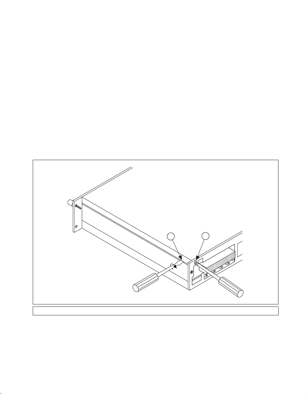
1. Remove the grounding screw from the module.
2. Remove the cover on the module to access the potentiometers.
) and the amplitude of the sine wave (Vs) so that Vs=3.4V
s
to a lower amplitude, but not a higher one. To prevent errors
s
rms/Gs
.
2
1 Grounding Screw 2 Module Cover
Figure 2. Grounding Screw and Cover Removal
© National Instruments Corporation 13 SCXI-1141/1142/1143 Calibration Procedure
1
Page 14

3. Remove the side plate of the SCXI chassis.
4. Install the module into slot 4 of the SCXI chassis.
®
S
C
X
I
M
A
I
N
F
R
A
M
E
NATIONAL
INSTRUMENTS
2
1
1 Thumbscrews 2Slot 4 3 Side Plate
Figure 3. Side Plate Removal and Module Installation
5. Read the Test Conditions section in this document.
6. Ensure that the E Series DAQ device is connected to the
SCXI-1141/1142/1143.
7. Call
SCXI_Set_Gain to configure the module to a gain value of 1.
Set the following parameters:
• SCXIchassisID—The device number assigned by MAX
• moduleSlot—4
• moduleChan—0
• gain—1
8. Call
SCXI_Configure_Filter to enable the filter bypass. Set the
following parameters:
• SCXIchassisID—The value configured in MAX
• moduleSlot—40
• channel—0
3
SCXI-1141/1142/1143 Calibration Procedure 14 ni.com
Page 15

• filterMode—0
• freq—0 kHz
• cutoffDivDown—0
• outClkDivDown—0
9. Connect the calibrator to analog input channel 0. Refer to Table 7
to determine the pins on the 96-pin front connector that correspond to
the positive and negative inputs of the specified channel. If you are
using an SCXI-1304 connected to the SCXI-1141/1142/1143, connect
the calibrator to the AI 0 + and AI 0 – inputs.
10. Connect the DMM to the output of channel 0. Refer to Table 8 to
determine the pins on the 50-pin rear connector that correspond to the
positive and negative outputs for the specified channel. For example,
the positive output for channel 0 is pin 3, which is AI 0 +. The negative
input for channel 0 is pin 4, which is AI 0 –.
11. Set the calibrator voltage to 3.4 V
, 400 Hz.
rms
12. Measure and record the amplitude of the sine wave with the DMM.
13. Call
SCXI_Configure_Filter to disable the filter bypass. Set the
following parameters:
• SCXIchassisID—The value configured in MAX
• moduleSlot—4
• channel—0
• filterMode—1
• freq—25 kHz
• cutoffDivDown—0
• outClkDivDown—2
14. Measure the amplitude of the sine wave at the output and adjust the
potentiometer until the amplitude is at the same level as it was with the
filter in bypass mode.
15. Repeat steps 8 through 14 for the remaining channels.
You have finished adjusting the filter AC gain of the
SCXI-1141/1142/1143.
SCXI-1141/1142/1143 Revision F or Later
Complete the following steps to adjust the AC gain of the filter on an
SCXI-1141/1142/1143 revision F or later:
1. Read the Test Conditions section in this document.
2. Ensure that the E Series DAQ device is connected to the
SCXI-1141/1142/1143.
© National Instruments Corporation 15 SCXI-1141/1142/1143 Calibration Procedure
Page 16

3. Call SCXI_Set_Gain to configure the module to a gain value of 1.
Set the following parameters:
• SCXIchassisID—The value obtained from MAX
• moduleSlot—4
• moduleChan—0
• gain—1
4. Call
SCXI_Configure_Filter to enable the filter bypass.
Set the following parameters:
• SCXIchassisID—The value obtained from MAX
• moduleSlot—4
• channel—0
• filterMode—0
• freq—0 kHz
• cutoffDivDown—0
• outClkDivDown—0
5. Connect the calibrator to analog input channel 0. Refer to Table 7 to
determine the pins on the 96-pin front connector that correspond to the
positive and negative inputs of the specified channel. If you are using
an SCXI-1304 that is connected to the SCXI-1141/1142/1143, connect
the calibrator to the AI 0 + and AI 0 – inputs.
6. Connect the DMM to the output of channel 0. Refer to Table 8 to
determine the pins on the 50-pin rear connector that correspond to the
positive and negative outputs for the specified channel. For example,
the positive output for channel 0 is pin 3, which is AI 0 +. The negative
input for channel 0 is pin 4, which is AI 0 –.
7. Set the calibrator voltage to 3.4 V
, 400 Hz.
rms
8. Measure and record the amplitude of the sine wave with the DMM.
9. Call
SCXI_Configure_Filter to enable the cutoff filter. Set the
following parameters:
• SCXIchassisID—The value obtained from MAX
• moduleSlot—4
• channel—0
• filterMode—1
• freq—25 kHz
• cutoffDivDown—0
• outClkDivDown—2
SCXI-1141/1142/1143 Calibration Procedure 16 ni.com
Page 17

10. Call the SCXI_SetDP function in SCXIdpCal.dll to set the digital
potentiometer to a neutral position, set the following short integer
parameters:
• SCXIchassisID—The value obtained from MAX
• moduleSlot—4
• channel—0
• value—127
11. Measure the amplitude of the sine wave at the output of the module.
12. If the measured value is less than the value measured with the filter
bypassed, increase the value to which the digital potentiometer is set.
If it is greater, decrease the value. You can set the digital potentiometer
from 0 to 255.
13. Call
14. Repeat steps 11 through 13 until the measured amplitude is as close as
15. Repeat steps 4 through 14 for the remaining channels.
SCXI_SetDP to set the digital potentiometer to the new value:
• SCXIchassisID—The value obtained from MAX
• moduleSlot—4
• channel—0
• value—The new value decided upon in step 12
possible to the level it was with the filter in bypass mode.
You have finished adjusting the filter AC gain of the
SCXI-1141/1142/1143.
Verifying Adjusted Values
After you complete the adjustment procedure, it is important that you verify
the accuracy of the adjusted values by repeating the procedure in the
Verifying the Operation of the SCXI-1141/1142/1143 section. Verifying
the adjusted values ensures that the SCXI-1141/1142/1143 is operating
within its specifications after adjustments.
Note If the module fails verification after adjustment, return it to NI for repair or
replacement.
Front and Rear Panel Pin Assignments
Table 7 shows the pin assignments for the SCXI-1141/1142/1143 front
panel connector.
© National Instruments Corporation 17 SCXI-1141/1142/1143 Calibration Procedure
Page 18
Table 7. Front Signal Pin Assignments
Front Connector Diagram Pin Number Column A Column B Column C
32 AI 0 + NC AI 0 –
Column
A B C
32
31
30
29
28
27
26
25
24
23
22
21
20
19
18
17
16
15
14
13
12
11
10
9
8
7
6
5
4
3
2
1
NC means no connection.
RSVD means reserved.
31 NC NC NC
30 AI 1 + NC AI 1 –
29 NC NC NC
28 A GND NC A GND
27 NC NC NC
26 AI 2 + NC AI 2 –
25 NC NC NC
24 AI 3 + NC AI 3 –
23 NC NC NC
22 A GND NC A GND
21 NC NC NC
20 AI 4 + NC AI 4 –
19 NC NC NC
18 AI 5 + NC AI 5 –
17 NC NC NC
16 A GND NC A GND
15 NC NC NC
14 AI 6 + NC AI 6 –
13 NC NC NC
12 AI 7 + NC AI 7 –
11 NC NC NC
10 NC NC NC
9 NC NC NC
8 RSVD NC RSVD
7 NC NC NC
6 RSVD NC RSVD
5 NC NC NC
4 RSVD NC EXT CLK
3 NC NC NC
2 D GND NC OUT CLK
1 NC NC NC
SCXI-1141/1142/1143 Calibration Procedure 18 ni.com
Page 19
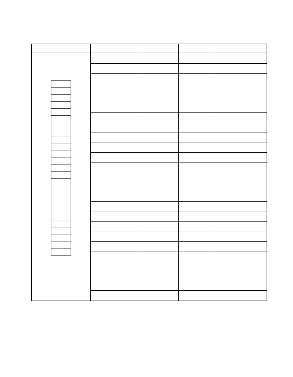
Table 8 shows the pin assignments for the SCXI-1141/1142/1143 rear
panel connector.
Table 8. Rear Signal Pin Assignments
Rear Connector Diagram Signal Name Pin Number Pin Number Signal Name
NC 1 2 NC
AI 0 + 3 4 AI 0 –
12
34
56
78
910
11 12
13 14
15 16
17 18
19 20
21 22
23 24
25 26
27 28
29 30
31 32
33 34
35 36
37 38
39 40
41 42
43 44
45 46
47 48
49 50
AI 1 + 5 6 A GND
AI 2 + 7 8 A GND
AI 3 + 9 10 A GND
AI 4 + 11 12 A GND
AI 5 + 13 14 A GND
AI 6 + 15 16 A GND
AI 7 + 17 18 A GND
NC 19 20 NC
NC 21 22 NC
NC 23 24 DIG GND
SER DAT IN 25 26 SER DAT OUT
DAQ D*/A 27 28 NC
SLOT 0 SEL* 29 30 NC
NC 31 32 NC
DIG GND 33 34 NC
NC 35 36 SCAN CLK
SER CLK 37 38 NC
NC 39 40 NC
NC 41 42 NC
RSVD 43 44 NC
NC 45 46 NC
NC means no connection.
RSVD means reserved.
© National Instruments Corporation 19 SCXI-1141/1142/1143 Calibration Procedure
NC 47 48 NC
NC 49 50 NC
Page 20
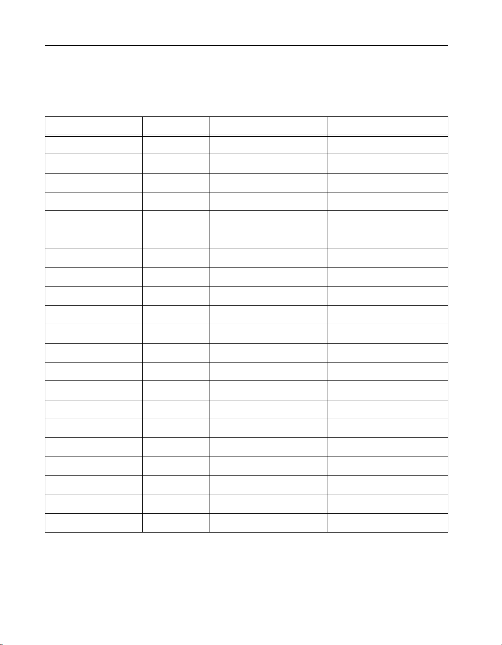
Specifications
Table 9 contains test specifications for the SCXI-1141/1142/1143. If the
module has been calibrated within the last year, the Test Point (V) value
should fall between the Upper Limit (V) and Lower Limit (V) values.
Table 9. SCXI-1141/1142/1143 Specifications
Test Point (V) Gain Upper Limit (V) Lower Limit (V)
4.7500 1 4.771715 4.728285
0.0000 1 0.020480 –0.020480
–4.7500 1 –4.728285 –4.771715
2.3750 2 2.390948 2.359052
0.0000 2 0.015330 –0.015330
–2.3750 2 –2.359052 –2.390948
0.9500 5 0.962487 0.937513
0.0000 5 0.012240 –0.012240
–0.9500 5 –0.937513 –0.962487
0.4750 10 0.486334 0.463666
0.0000 10 0.011210 –0.011210
–0.4750 10 –0.463666 –0.486334
0.2375 20 0.248258 0.226742
0.0000 20 0.010696 –0.010696
–0.2375 20 –0.226742 –0.248258
0.0750 50 0.085408 0.064592
0.0000 50 0.010388 –0.010388
–0.0750 50 –0.064592 –0.085408
0.0375 100 0.047796 0.027204
0.0000 100 0.010286 –0.010286
–0.0375 100 –0.027204 –0.047796
National Instruments, NI, ni.com, and LabVIEW are trademarks of National Instruments Corporation.
Refer to the Terms of Use section on ni.com/legal for more information about National
Instruments trademarks. Other product and company names mentioned herein are trademarks or trad e
names of their respective companies. For patents covering National Instruments products, refer to the
appropriate location: Help»Patents in your software, the patents.txt file on your CD, or
ni.com/patents.
© 2000–2007 National Instruments Corporation. All rights reserved.
370156C-01 Mar07
 Loading...