

Page 1

TM
SCXI -1122
User Manual
Sixteen-Channel Isolated Transducer Multiplexer Module for Signal
Conditioning
September 1999 Edition
Part Number 320516B-01
© Copyright 1993, 1999 National Instruments Corporation.
All Rights Reserved.
Page 2

Worldwide Technical Support and Product Information
www.natinst.com
National Instruments Corporate Headquarters
11500 North Mopac Expressway Austin, Texas 78759-3504 USA Tel: 512 794 0100
Worldwide Offices
Australia 03 9879 5166, Austria 0662 45 79 90 0, Belgium 02 757 00 20, Brazil 011 284 5011, Canada (Calgary) 403 274 9391,
Canada (Ontario) 905 785 0085, Canada (Québec) 514 694 8521, China 0755 3904939, Denmark 45 76 26 00,
Finland 09 725 725 11, France 01 48 14 24 24, Greece 30 1 42 96 427, Germany 089 741 31 30, Hong Kong 2645 3186,
India 91805275406, Israel 03 6120092, Italy 02 413091, Japan 03 5472 2970, Korea 02 596 7456, Mexico (D.F.) 5 280 7625,
Mexico (Monterrey) 8 357 7695, Netherlands 0348 433466, Norway 32 27 73 00, Singapore 2265886,
Spain (Barcelona) 93 582 0251, Spain (Madrid) 91 640 0085, Sweden 08 587 895 00, Switzerland 056 200 51 51,
Taiwan 02 377 1200, United Kingdom 01635 523545
Page 3

Warranty
The SCXI-1122 is warranted against defects in mat erials and workmans hip for a period of one year from the date of
shipment, as evidenced by receipts or other documentation. National Instruments will, at its option, repair or replace
equipment that proves to be defective during the warranty period. This warranty includes parts and labor.
A Return Material Authorization (RMA) number must be obtained from the factory and clearly marked on the
outside of thepackage before any equipment will be accepted for warranty work. National Instruments will pay the
shipping costs of returning to the ow ner part s whic h are covere d by w arra nty.
National Instruments believes that the information in this document is accurate. The document has been carefully
reviewed fortechnical accuracy. In the event that technical or typographical errors exist, National Instruments
reserves the right to makechanges to subsequent editions of this document without prior notice to holders of this
edition. The reader should consult National Instruments if errors are suspected. In no event shall National
Instruments be liable for any damages arising out of orrelated to this document or the information contained in it.
E
XCEPT AS SPECIFIED HEREIN
SPECIFICALLY DISCLAIMS ANY WARRANTY OF MERCHANTABILITY OR FITNESS FOR A PARTICULAR PURPOSE
C
USTOMER’S RIGHT TO RECOVER DAMAGES CAUSED BY FAULT OR NEGLIGENCE ON THE PART OF NATIONAL
I
NSTRUMENTS SHALL BE LIMITED TO THE AMOUNT THERETOFORE PAID BY THE CUSTOMER
I
NSTRUMENTS WILL NOT BE LIABLE FOR DAMAGES RESULTING FROM LOSS OF DATA, PROFITS, USE OF PRODUCTS, OR
INCIDENTAL OR CONSEQUENTIAL DAMAGES, EVEN IF ADVISED OF THE POSSIBILITY THEREOF
, N
ATIONAL INSTRUMENTS MAKES NO WARRANTIES, EXPRESS OR IMPLIED, AND
. N
ATIONAL
. This limitation of the
.
liability of National Instruments will apply regardless of the form of action, whether in contract or tort, including
negligence. Anyaction against National Instruments must be brought within one year after the cause of action
accrues. National Instruments shall not be liable for anydelay in performance due to causes beyond its reasonable
control. The warranty provided h erein d oes no t cover d amages, defects, m alfunctions , or se rvice failures caused by
owner’s failure to follow the National Instruments installation, operation, or maintenance instructions; owner’s
modification of the product; ow ner’s abuse , misuse , or ne glige nt a cts; and powe r failure or surges , fire , flood,
accident, actions of third parties, orotherevents outside reasonable control.
Copyright
Under the copyright laws, this publication may not be reproduced or transmitted in any form, electronic or
mechanical, including photocopying, recording, storing in an information retrieval system, or translating, in whole
or in part, without theprior written consent of National Instruments Corporation.
Trademarks
LabVIEW™, NI-DAQ™, natinst.com™, National Instruments™, RTSI™, and SCXI™ are trademarks of
NationalInstrume nts Cor por at ion.
Product and company names mentioned herein are trademarks or trade names of their respective companies.
Page 4

WARNING REGARDING USE OF NATIONAL INSTRUMENTS PRODUCTS
(1) NATIONAL INSTRUMENTS PRODUCTS ARE NOT DESIGNED WITH COMPONENTS AND TESTING
FOR A LEVEL OF RELIABILITY SUITABLE FOR USE IN OR IN CONNECTION WITH SURGICAL
IMPLANTS OR AS CRITICAL COMPONENTS IN ANY LIFE SUPPORT SYSTEMS WHOSE FAILURE TO
PERFORM CAN REASONABLY BE EXPECTED TO CAUSE SIGNIFICANT INJURY TO A HUMAN.
(2) IN ANY APPLICATION, INCLUDING THE ABOVE, RELIABILITY OF OPERATION OF THE
SOFTWARE PRODUCTS CAN BE IMPAIRED BY ADVERSE FACTORS, INCLUDING BUT NOT LIMITED
TO FLUCTUATIONS IN ELECTRICAL POWER SUPPLY, COMPUTER HARDWARE MALFUNCTIONS,
COMPUTER OPERATING SYSTEM SOFTWARE FITNESS, FITNESS OF COMPILERS AND
DEVELOPMENT SOFTWARE USED TO DEVELOP AN APPLICATION, INSTALLATION ERRORS,
SOFTWARE AND HARDWARE COMPATIBILITY PROBLEMS, MALFUNCTIONS OR FAILURES OF
ELECTRONIC MONITORING OR CONTROL DEVICES, TRANSIENT FAILURES OF ELECTRONIC
SYSTEMS (HARDWARE AND/OR SOFTWARE), UNANTICIPATED USES OR MISUSES, OR ERRORS ON
THE PART OF THE USER OR APPLICATIONS DESIGNER (ADVERSE FACTORS SUCH AS THESE ARE
HEREAFTER COLLECTIVELY TERMED “SYSTEM FAILURES”). ANY APPLICATION WHERE A
SYSTEM FAILURE WOULD CREATE A RISK OF HARM TO PROPERTY OR PERSONS (INCLUDING THE
RISK OF BODILY INJURY AND DEATH) SHOULD NOT BE RELIANT SOLELY UPON ONE FORM OF
ELECTRONIC SYSTEM DUE TO THE RISK OF SYSTEM FAILURE. TO AVOID DAMAGE, INJURY, OR
DEATH, THE USER OR APPLICATION DESIGNER MUST TAKE REASONABLY PRUDENT STEPS TO
PROTECT AGAINST SYSTEM FAILURES, INCLUDING BUT NOT LIMITED TO BACK-UP OR SHUT
DOWN MECHANISMS. BECAUSE EACH END-USER SYSTEM IS CUSTOMIZED AND DIFFERS FROM
NATIONAL INSTRUMENTS' TESTING PLATFORMS AND BECAUSE A USER OR APPLICATION
DESIGNER MAY USE NATIONAL INSTRUMENTS PRODUCTS IN COMBINATION WITH OTHER
PRODUCTS IN A MANNER NOT EVALUATED OR CONTEMPLATED BY NATIONAL INSTRUMENTS,
THE USER OR APPLICATION DESIGNER IS ULTIMATELY RESPONSIBLE FOR VERIFYING AND
VALIDATING THE SUITABILITY OF NATIONAL INSTRUMENTS PRODUCTS WHENEVER NATIONAL
INSTRUMENTS PRODUCTS ARE INCORPORATED IN A SYSTEM OR APPLICATION, INCLUDING,
WITHOUT LIMITATION, THE APPROPRIATE DESIGN, PROCESS AND SAFETY LEVEL OF SUCH
SYSTEM OR APPLICATION.
Page 5

Contents
About This Manual............................................................................................................. ix
Organization of This Manual ......................................................................................... ix
Conventions Used in This Manual................................................................................. x
The National Instruments Documentation Set............................................................... xi
Related Documentation.................................................................................................. xi
Customer Communication ............................................................................................. xii
Chapter 1
Introduction
What Your Kit Should Contain...................................................................................... 1-1
Software Programming Choices .................................................................................... 1-2
Optional Equipment ....................................................................................................... 1-4
Unpacking ...................................................................................................................... 1-5
Chapter 2
Configuration and Installation
Module Configuration.................................................................................................... 2-1
Hardware Installation..................................................................................................... 2-6
.......................................................................................................................... 1-1
LabVIEW and LabWindows Application Software .......................................... 1-2
NI-DAQ Driver Software................................................................................... 1-2
Register-Level Programming............................................................................. 1-4
Custom Cables ................................................................................................... 1-5
....................................................................................... 2-1
Digital Signal Connections ................................................................................ 2-3
Analog Configuration ........................................................................................ 2-3
Current-Loop Receivers......................................................................... 2-4
Chapter 3
Signal Connections
Front Connector ............................................................................................................. 3-3
Front Signal Connection Descriptions ............................................................... 3-4
Analog Input Channel Signal Connections............................................ 3-5
Excitation Channel Signal Connections................................................. 3-8
Temperature Sensor Connection........................................................................ 3-9
Rear Signal Connector ................................................................................................... 3-10
Rear Signal Connection Descriptions ................................................................ 3-11
Analog Output Signal Connections........................................................ 3-11
Digital I/O Signal Connections.............................................................. 3-12
Chapter 4
Theory of Operation
Functional Overview...................................................................................................... 4-1
Rear Signal Connector, SCXIbus Connector, and SCXIbus Interface .............. 4-3
Digital Control Circuitry.................................................................................... 4-3
Analog Circuitry ................................................................................................ 4-3
Analog Input Channels........................................................................... 4-3
Excitation Output Channels ................................................................... 4-5
............................................................................................................. 3-1
Excitation Level ......................................................................... 3-8
Using the Internal Half-Bridge Completion............................... 3-9
.......................................................................................................... 4-1
© National Instruments Corporation v SCXI-1122 User Manual
Page 6

Contents
Chapter 5
Calibration
Overview........................................................................................................................ 5-1
Calibration Procedure .................................................................................................... 5-1
............................................................................................................................. 5-1
Calibration Equipment Requirements................................................................ 5-1
Gain and Offset Calibration ............................................................................... 5-2
Excitation Calibration ........................................................................................ 5-4
Appendix A
Specifications
Analog Input .................................................................................................................. A-1
Excitation ....................................................................................................................... A-3
Physical .......................................................................................................................... A-3
Environment................................................................................................................... A-3
........................................................................................................................ A-1
Appendix B
Customer Communication
............................................................................................... B-1
Glossary...................................................................................................................... Glossary-1
Index ................................................................................................................................ Index-1
SCXI-1122 User Manual vi © National Instruments Corporation
Page 7

Contents
Figures
Figure1-1. The Relationship between the Programming Environment, NI-DAQ, and
Your Hardware................................................................................................... 1-3
Figure2-1. SCXI-1122 Parts Locator Diagram.................................................................... 2-2
Figure3-1. SCXI-1122 Front Connector Pin Assignments.................................................. 3-3
Figure3-2. Ground-Referenced Signal Connection with High Common-Mode Voltage.... 3-6
Figure3-3. Floating Signal Connection Referenced to Chassis Ground for Better SNR..... 3-6
Figure3-4. Floating AC-Coupled Signal Connection Referenced
to Chassis Ground for Better SNR..................................................................... 3-6
Figure3-5. AC-Coupled Signal Connection with High Common-Mode Voltage............... 3-7
Figure3-6. Avoiding Relay Wear by Sampling and Averaging Rather Than
Single-Sample Channel Scanning...................................................................... 3-8
Figure3-7. Connecting a Quarter-Bridge Strain Gauge to Channel 0.................................. 3-9
Figure3-8. SCXI-1122 Rear Signal Connector Pin Assignments........................................ 3-10
Figure4-1. SCXI-1122 Block Diagram................................................................................ 4-2
Figure4-2. Series Connection with Current Excitation........................................................ 4-6
Figure4-3. Four-Wire Scan Connection with Multiplexed Current Excitation................... 4-6
Tables
Table2-1. Digital Signal Connection Jumper Settings....................................................... 2-3
Table2-2. Jumper W1 Settings........................................................................................... 2-4
Table2-3. User-Defined Current Receiver Resistors.......................................................... 2-4
Table3-1. Maximum Load per Excitation Channel............................................................ 3-9
Table3-2. SCXIbus to SCXI-1122 Rear Signal Connector to DAQ Board Pin
Equivalences...................................................................................................... 3-13
Table4-1. Sense/Current Output Channel Associations..................................................... 4-4
Table4-2. Pros and Cons of Two-Wire and Four-Wire Connections
with Current Excited Transducers...................................................................... 4-7
Table5-1. Maximum Allowable Error Ranges................................................................... 5-4
© National Instruments Corporation vii SCXI-1122 User Manual
Page 8

About This Manual
This manual describes the electrical and mechanical aspects of the SCXI-1122 and contains
information concerning its operation. The SCXI-1122 is a member of the National Instruments
Signal Conditioning eXtensions for Instrumentation (SCXI) Series for the National Instruments
DAQ plug-in boards. This module is designed for signal conditioning of strain gauges, RTDs,
thermistors, thermocouples, volt and millivolt sources, and 4 to 20 mA sources or 0 to 20 mA
process-current sources where high common-mode voltages exist. The SCXI-1122 operates as 16
isolated input channels, one isolated current excitation channel, and one voltage excitation channel.
All 16 channels are isolated from earth ground but not from each other. The excitation circuits are
both isolated from earth ground, the input channels, and between each other.
Organization of This Manual
The SCXI-1122 User Manual is organized as follows:
Chapter 1, Introduction, describes the SCXI-1122; lists the contents of your SCXI-1122 kit;
describes the optional software, optional equipment, and custom cables; and explains how to
unpack the SCXI-1122.
Chapter 2, Configuration and Installation, describes how to configure the SCXI-1122
jumpers and how to install the SCXI-1122 into the SCXI chassis.
Chapter 3, Signal Connections, describes the input and output signal connections to the
SCXI-1122 module via the SCXI-1122 front connector and rear signal connector. This
chapter also includes specifications and connection instructions for the signals on the
SCXI-1122 connectors.
Chapter 4, Theory of Operation, contains a functional overview of the SCXI-1122 module
and explains the operation of each functional unit making up the SCXI-1122.
Chapter 5, Calibration, discusses the calibration procedures for the SCXI-1122.
Appendix A, Specifications, lists the specifications for the SCXI-1122.
Appendix B, Customer Communication, contains forms you can use to request help from
National Instruments or to comment on our products.
The Glossary contains an alphabetical list and description of terms used in this manual,
including abbreviations, acronyms, metric prefixes, mnemonics, symbols, and terms.
The Index contains an alphabetical list of key terms and topics in this manual, including the
page where you can find each one.
© National Instruments Corporation ix SCXI-1122 User Manual
Page 9

About This Manual
Conventions Used in This Manual
The following conventions are used in this manual.
!
bold italic Bold italic text denotes a note, caution, or warning.
italic Italic text denotes emphasis, a cross reference, or an introduction to a key
Lab board Lab board refers to the Lab-LC, Lab-NB, Lab-PC, and Lab-PC+ boards
MC MC refers to the Micro Channel series computers.
MIO board MIO board refers to the National Instruments multichannel I/O DAQ
monospace Lowercase text in this font denotes text or characters that are to be literally
This symbol refers to a caution that must be taken when operating this
equipment. This symbol is found on the equipment and near the explanation of
the caution in the manual.
concept.
unless otherwise noted.
boards, AT-MIO-16, MC-MIO-16, AT-MIO-16F-5,
AT-MIO-16X, AT-MIO-16D, AT-MIO-64F-5, NB-MIO-16, and
NB-MIO-16X, unless otherwise noted.
input from the keyboard, sections of code, programming examples, and
syntax examples. This font is also used for the proper names of disk
drives, paths, directories, programs, subprograms, subroutines, device
names, functions, variables, filenames, and extensions, and for statements
and comments taken from program code.
NB NB refers to the NuBus series computers.
PC PC refers to the IBM PC/XT, the IBM PC AT, and compatible computers.
SCXIbus SCXIbus refers to the backplane in the chassis. A signal on the backplane
is referred to as the SCXIbus <signal name> line (or signal). The
SCXIbus descriptor may be omitted when the meaning is clear.
Descriptions of all SCXIbus signals are in Chapter 3, Signal Connections.
Slot 0 Slot 0 refers to the power supply and control circuitry in the SCXI chassis.
Abbreviations, acronyms, metric prefixes, mnemonics, symbols, and terms are listed in the
Glossary.
SCXI-1122 User Manual x © National Instruments Corporation
Page 10

About This Manual
The National Instruments Documentation Set
The SCXI-1122 User Manual is one piece of the documentation set for your SCXI system. You
should have six types of manuals. Use these different types of manuals as follows:
• Getting Started with SCXI–This is the first manual you should read. It gives an overview of
the SCXI system and contains the most commonly needed information for the modules,
chassis, and software.
• Your SCXI module user manuals–These manuals contain detailed information about signals
connections and module configuration. They also explain in greater detail how the module
works and application hints.
• Your DAQ board user manuals–These manuals have detailed information about the DAQ
board that plugs into your computer. Use these manuals for board installation and
configuration instructions, specification information about your DAQ board, and application
hints.
• Software manuals–Examples of software manuals you might have are the LabVIEW and
LabWindows
system, use either the application software (LabVIEW or LabWindows) manuals or the
NI-DAQ manuals to help you write your application. If you have a large and complicated
system, it is worthwhile to look through the software manuals before you configure your
hardware.
®
manual sets and the NI-DAQ manuals. After you have set up your hardware
• Accessory manuals–These are the terminal block and cable assembly installation guides.
They explain how to physically connect the relevant pieces of the system together. Consult
these when you are making your connections.
• SCXI chassis manuals–These manuals contain maintenance information on the chassis,
installation instructions, and information for making custom modules.
Related Documentation
The following National Instruments manual contains detailed information for the register-level
programmer:
• SCXI-1122 Register-Level Programmer Manual (part number 340696-01)
This manual is available from National Instruments by request. If you are using NI-DAQ,
LabVIEW, or LabWindows, you should not need the register-level programmer manual. Using
NI-DAQ, LabVIEW, or LabWindows is quicker and easier than and as flexible as using the lowlevel programming described in the register-level programmer manual. Refer to Software
Programming Choices in Chapter 1, Introduction, of this manual to learn about your
programming options.
© National Instruments Corporation xi SCXI-1122 User Manual
Page 11

About This Manual
Customer Communication
National Instruments wants to receive your comments on our products and manuals. We are
interested in the applications you develop with our products, and we want to help if you have
problems with them. To make it easy for you to contact us, this manual contains comment and
configuration forms for you to complete. These forms are in Appendix B, Customer
Communication, at the end of this manual.
SCXI-1122 User Manual xii © National Instruments Corporation
Page 12

Chapter 1 Introduction
This chapter describes the SCXI-1122; lists the contents of your SCXI-1122 kit; describes the
optional software, optional equipment, and custom cables; and explains how to unpack the
SCXI-1122.
The SCXI-1122 has 16 isolated input channels and two isolated excitation channels. The
SCXI-1122 is a module for signal conditioning of strain gauges, RTDs, thermistors,
thermocouples, volt and millivolt sources, 4 to 20 mA current sources, and 0 to 20 mA processcurrent sources. The SCXI-1122 can operate in two modes–two-wire scan mode with all 16
input channels used for input, or the four-wire scan mode with the eight upper channels
configured as sense leads for connecting inputs and the lower eight channels configured as
current output channels. The SCXI-1122 inputs are multiplexed to a single output, which drives
a single DAQ board channel.
The SCXI-1122 operates with full functionality with the National Instruments MIO-16,
Lab-PC+, and the SCXI-1200 boards. You can use the Lab and PC-LPM-16 boards with the
SCXI-1122, but these boards cannot scan the module. These boards can perform only singlechannel reads. You can multiplex several SCXI-1122s into a single channel, thus greatly
increasing the number of isolated analog input signals that you can digitize.
You can add the SCXI-1322 shielded terminal block, which has screw terminals to which you
can easily attach the input signals to the SCXI-1122. In addition, the SCXI-1322 has a
temperature sensor for cold-junction compensation of thermocouples. This cold-junction
reference (CJR) is multiplexed with the 16 input channels.
What Your Kit Should Contain
The contents of the SCXI-1122 kit (part number 776572-22) are listed as follows:
Kit Component Part Number
SCXI-1122 module 182366-01
SCXI-1122 User Manual 320516-01
If your kit is missing any of the components, contact National Instruments.
Detailed specifications of the SCXI-1122 are listed in Appendix A, Specifications.
© National Instruments Corporation 1-1 SCXI-1122 User Manual
Page 13

Introduction Chapter 1
Software Programming Choices
There are four options to choose from when programming your National Instruments plug-in
DAQ board and SCXI hardware. You can use LabVIEW, LabWindows, NI-DAQ, or registerlevel programming software.
LabVIEW and LabWindows Application Software
LabVIEW and LabWindows are innovative program development software packages for data
acquisition and control applications. LabVIEW uses graphical programming, whereas
LabWindows enhances traditional programming languages. Both packages include extensive
libraries for data acquisition, instrument control, data analysis, and graphical data presentation.
LabVIEW currently runs on three different platforms–AT/MC/EISA computers running
Microsoft Windows, the Macintosh platform, and the Sun SPARCstation platform. LabVIEW
features interactive graphics, a state-of-the-art user interface, and a powerful graphical
programming language. The LabVIEW Data Acquisition VI Library, a series of VIs for using
LabVIEW with National Instruments boards, is included with LabVIEW. The LabVIEW Data
Acquisition VI Libraries are functionally equivalent to the NI-DAQ software.
LabWindows has two versions–LabWindows for DOS is for use on PCs running DOS, and
LabWindows/CVI is for use on PCs running Windows and Sun SPARCstations.
LabWindows/CVI features interactive graphics, a state-of-the-art user interface, and uses the
ANSI standard C programming language. The LabWindows Data Acquisition Library, a series
of functions for using LabWindows with National Instruments boards, is included with
LabWindows for DOS and LabWindows/CVI. The LabWindows Data Acquisition libraries are
functionally equivalent to the NI-DAQ software.
Using LabVIEW or LabWindows software will greatly diminish the development time for your
data acquisition and control application. Part numbers for these software products are as follows:
Software Part Number
LabVIEW for Windows 776670-01
LabVIEW for Macintosh 776141-01
LabWindows for DOS 776475-01
LabWindows/CVI for Windows 776800-01
NI-DAQ Driver Software
The NI-DAQ driver software is included at no charge with all National Instruments DAQ boards.
NI-DAQ has an extensive library of functions that you can call from your application
programming environment. These functions include routines for analog input (A/D conversion),
buffered data acquisition (high-speed A/D conversion), analog output (D/A conversion),
waveform generation, digital I/O, counter/timer operations, SCXI, RTSI, self-calibration,
messaging, and acquiring data to extended memory.
SCXI-1122 User Manual 1-2 © National Instruments Corporation
Page 14

Chapter 1 Introduction
NI-DAQ also internally addresses many of the complex issues between the computer and the
plug-in board such as programming interrupts and DMA controllers. NI-DAQ maintains a
consistent software interface among its different versions so that you can change platforms with
minimal modifications to your code. Figure 1-1 illustrates the relationship between NI-DAQ and
LabVIEW and LabWindows. You can see that the data acquisition parts of LabVIEW and
LabWindows are functionally equivalent to the NI-DAQ software.
Conventional
Programming
Environment
(PC or Macintosh)
LabVIEW
(PC or Macintosh)
NI-DAQ
Driver Software
LabWindows
(PC)
Data Acquisition
Boards or
SCXI Hardware
Personal
Computer
or
Workstation
Figure 1-1. The Relationship between the Programming Environment,
NI-DAQ, and Your Hardware
The National Instruments PC, AT, and MC Series DAQ boards are packaged with NI-DAQ
software for PC compatibles. NI-DAQ software for PC compatibles comes with language
interfaces for Professional BASIC, Turbo Pascal, Turbo C, Turbo C++, Borland C++, and
Microsoft C for DOS; and Visual Basic, Turbo Pascal, Microsoft C with SDK, and Borland C++
for Windows. You can use your SCXI-1122, together with other PC, AT, and MC Series DAQ
boards and SCXI hardware, with NI-DAQ software for PC compatibles.
The National Instruments NB Series DAQ boards are packaged with NI-DAQ software for
Macintosh. NI-DAQ software for Macintosh comes with language interfaces for MPW C,
THINK C, Pascal, and Microsoft QuickBASIC. Any language that uses Device Manager
Toolbox calls can access NI-DAQ software for Macintosh. You can use NB Series DAQ boards
and SCXI hardware with NI-DAQ software for Macintosh.
© National Instruments Corporation 1-3 SCXI-1122 User Manual
Page 15

Introduction Chapter 1
Register-Level Programming
The final option for programming any National Instruments DAQ hardware is to write registerlevel software. Writing register-level programming software can be very time consuming and
inefficient, and is not recommended for most users. The only users who should consider writing
register-level software should meet at least one of the following criteria:
• National Instruments does not support your operating system or programming language.
• You are an experienced register-level programmer who is more comfortable writing your
own register-level software.
Always consider using NI-DAQ, LabVIEW, or LabWindows to program your National
Instruments DAQ hardware. Using the NI-DAQ, LabVIEW, or LabWindows software is easier
than and as flexible as register-level programming, and can save you weeks of development time.
The SCXI-1122 User Manual and your software manuals contain complete instructions for
programming your DAQ board with NI-DAQ, LabVIEW, or LabWindows. If you are using
NI-DAQ, LabVIEW, or LabWindows to control your board, you should not need the registerlevel programmer manual. The SCXI-1122 Register-Level Programmer Manual contains lowlevel programming details, such as register maps, bit descriptions, and register programming
hints, that you will need only for register-level programming. Some hardware user manuals
include register map descriptions and register programming hints. If your manual does not
contain a register map description and you want to obtain the register-level programmer manual,
please fill out the Register-Level Programmer Manual Request Form at the end of this manual
and send it to National Instruments.
Optional Equipment
Equipment Part Number
SCXI-1322 front terminal block 776573-22
SCXI-1340 cable assembly 776574-40
SCXI-1341 Lab-NB/Lab-PC/Lab-PC+ cable assembly 776574-41
SCXI-1342 PC-LPM-16 cable assembly 776574-42
SCXI-1343 rear screw terminal adapter 776574-43
SCXI-1344 Lab-LC cable assembly 776574-44
SCXI-1345 shielded cable with adapter, 1 m
2 m
5 m
10 m
SCXI-1350 multichassis adapter 776575-50
SCXI process-current resistor kit
Standard ribbon cable, 0.5 m
1.0 m
1 Resistor kit needed to perform current measurements. (See pages 2-4)
Refer to Chapter 3, Signal Connections, and to your cable installation guide for additional
information on cabling, connectors, and adapters.
1
776574-451
776574-452
776574-455
776574-450
776582-01
180524-05
180524-10
SCXI-1122 User Manual 1-4 © National Instruments Corporation
Page 16

Chapter 1 Introduction
Custom Cables
The SCXI-1122 rear signal connector is a 50-pin male ribbon-cable header. The manufacturer
part number that National Instruments uses for this header is as follows:
• AMP Inc. (part number 1-103310-0)
The mating connector for the SCXI-1122 rear signal connector is a 50-position polarized
ribbon-socket connector with strain relief. National Instruments uses a polarized or keyed
connector to prevent inadvertent upside-down connection to the SCXI-1122. Recommended
manufacturer part numbers for this mating connector are as follows:
• Electronic Products Division/3M (part number 3425-7650)
• T&B/Ansley Corporation (part number 609-5041CE)
Standard 50-conductor, 28 AWG, stranded ribbon cables that you can use with these connectors
are as follows:
• Electronic Products Division/3M (part number 3365/50)
• T&B/Ansley Corporation (part number 171-50)
The SCXI-1122 front connector is a 48-pin DIN C male connector. The manufacturer part
number that National Instruments uses for this connector is as follows:
• ERNI (part number 913523)
The mating connector for the SCXI-1122 front connector is a 48-pin DIN C female connector.
National Instruments uses a polarized connector to prevent inadvertent upside-down connection
to the SCXI-1122. The manufacturer part number that National Instruments uses for this
connector is as follows:
• ERNI (part number 913524; right-angle pins)
Unpacking
Your SCXI-1122 module is shipped in an antistatic package to prevent electrostatic damage to
the module. Electrostatic discharge can damage several components on the module. To avoid
such damage in handling the module, take the following precautions.
• Ground yourself via a grounding strap or by holding a grounded chassis such as your SCXI
chassis.
• Touch the antistatic package to a metal part of your SCXI chassis before removing the
module from the package.
• Remove the module from the package and inspect the module for loose components or any
other sign of damage. Notify National Instruments if the module appears damaged in any
way. Do not install a damaged module into your SCXI chassis.
• Never touch the exposed pins of connectors.
© National Instruments Corporation 1-5 SCXI-1122 User Manual
Page 17

Chapter 2 Configuration and Installation
This chapter describes how to configure the SCXI-1122 jumpers and how to install the
SCXI-1122 into the SCXI chassis.
Module Configuration
The SCXI-1122 contains two jumpers that are shown in the parts locator diagram in Figure 2-1.
Jumper W2 connects a pullup resistor to the SERDATOUT signal on the rear signal connector.
Jumper W1 configures the guard and the analog output ground, and enables the
pseudodifferential reference mode.
You must use software to further configure the module. Refer to your software manuals, or to
the SCXI-1122 Register-Level Programmer Manual if you are a register-level programmer.
© National Instruments Corporation 2-1 SCXI-1122 User Manual
Page 18

Configuration and Installation Chapter 2
Figure 2-1. SCXI-1122 Parts Locator Diagram
SCXI-1122 User Manual 2-2 © National Instruments Corporation
Page 19

Chapter 2 Configuration and Installation
Digital Signal Connections
Note: If nothing is cabled to the SCXI-1122 rear signal connector, the position of
jumper W2 is irrelevant.
The SCXI-1122 has one jumper–jumper W2–for communication between the DAQ board and
the SCXIbus, shown in Table 2-1.
Table 2-1. Digital Signal Connection Jumper Settings
Jumper Description Configuration
DAQ board to
SCXIbus
communication
W2
Position 1 (pullup)–Use this setting
for a single-chassis system.
Connects a 2.2 kΩ pullup resistor to
the SERDATOUT line. (factory
setting)
Position 3 (unmarked position, no
pullup)–Use this setting for
additional chassis in a multichassis
system. No pullup resistor is
connected to the SERDATOUT line.
W2
1
W2
1
If a module is not connected to a DAQ board, the position of W2 is irrelevant. The MISO line
on the SCXI-1122 module is for reading the Module ID Register, the Status Register, and the
EEPROM. National Instruments software does not read the Module ID automatically–you must
indicate to the software which module is in which slot.
An open-collector driver (a driver that actively drives low or goes to high-impedance state,
relying on a pullup resistor to make the signal line go high) drives the SERDATOUT line. When
using a single chassis, set jumper W2 in position 1 on the SCXI-1122 that is connected to the
DAQ board. In this setting, the module drives MISO to SERDATOUT and connects the
necessary pullup resistor to the SERDATOUT line. When using multiple chassis, set jumper W2
to position 1 on only one of the SCXI-1122s that are cabled to the DAQ board. It does not
matter which of the SCXI-1122s that are cabled to the DAQ board has the pullup connected. Set
jumper W2 in position 3 on all of the other SCXI-1122 modules that are cabled to the DAQ
board because if too many pullup resistors are attached to the SERDATOUT line, the drivers
cannot drive the line low.
Analog Configuration
The SCXI-1122 has one analog configuration jumper–jumper W1–for grounding, shielding, and
reference mode selection, shown in Table 2-2.
© National Instruments Corporation 2-3 SCXI-1122 User Manual
Page 20

Configuration and Installation Chapter 2
Table 2-2. Jumper W1 Settings
Jumper Description Configuration
Grounding,
shielding, and
reference mode
selection
Unconnected position (factory setting)
Connects the analog reference to the
analog output ground AOGND (pins 1
and 2 on the rear signal connector).
Select this configuration if you are
B
A
R1 R2
R0
B
A
R1 R2
R0
W1
W1
using an RSE DAQ board. Do not use
a differential input DAQ board when
jumper W1 is in this position.
B
A
R1 R2
R0
B
A
R1 R2
R0
W1
W1
W1
Connects SCXIbus guard to the analog
reference
Enables the pseudodifferential
reference mode and connects the
analog reference to the OUTREF pin
on the rear signal connector. Select
this mode when the SCXI-1122 has to
operate with DAQ boards that have a
nonreferenced single-ended (NRSE)
input. Do not use differential input
DAQ boards when jumper W1 is in
this position.
Current-Loop Receivers
The SCXI-1122 has pads for transforming individual channels to current-to-voltage converters.
National Instruments offers an SCXI process current pack, which consists of a package of four
249 Ω, 0.1%, 5 ppm, 1/4 W resistors. You can find the part number for this kit in the Optional
Equipment section of Chapter 1, Introduction. Table 2-3 shows the input channel and its
corresponding resistor reference designator.
Table 2-3. User-Defined Current Receiver Resistors
Input Channel Resistor Reference Designator
0R1
1R2
2R3
3R4
(continues)
SCXI-1122 User Manual 2-4 © National Instruments Corporation
Page 21

Chapter 2 Configuration and Installation
Table 2-3. User-Defined Current Receiver Resistors (Continued)
Input Channel Resistor Reference Designator
4R5
5R6
6R7
7R8
8R9
9 R10
10 R11
11 R12
12 R13
13 R14
14 R17
15 R18
Warning: Before installing the resistors in your module, make sure that there are no signals
connected to your module front connector.
!
SHOCK HAZARD–This unit should only be opened by qualified personnel aware of
the dangers involved. Disconnect all power before removing the cover. Always
install the grounding screw. If signal wires are connected to the module or
terminal block, dangerous voltages may exist even when the equipment is turned
off. Before you remove any installed module, disconnect the AC power line or
any high-voltage sources (
≥
30 Vrms, 42.4 Vpk or 60 Vdc) that may be connected
to the module.
To install the resistors, you need to do the following before installing your module in the SCXI
chassis:
1. Ground yourself via a grounding strap or via a ground connected to your SCXI chassis.
Properly grounding yourself prevents damage to your SCXI module from electrostatic
discharge.
2. Remove the module cover by unscrewing the grounding screw at the rear of the module.
3. Remove the rear panel by unscrewing the two remaining screws.
4. Slide the module out of its enclosure.
5. Insert the resistor(s) into the appropriate pad.
6. Solder the leads to the pads on the solder side of the module.
7. Trim the leads to 0.06 in. maximum.
8. Slide the module back into its enclosure.
9. Reinstall the rear panel.
10. Reinstall the top cover and grounding screw.
11. Your module is ready to be installed into the chassis.
© National Instruments Corporation 2-5 SCXI-1122 User Manual
Page 22

Configuration and Installation Chapter 2
Hardware Installation
You can install the SCXI-1122 in any available SCXI chassis slot. After you have made any
necessary changes and have verified and recorded the jumper settings on the form in
Appendix B, Customer Communication, you are ready to install the SCXI-1122. The following
are general installation instructions; consult the user manual or technical reference manual of
your SCXI chassis for specific instructions and warnings.
1. Turn off the computer that contains the DAQ board or disconnect it from your SCXI chassis.
2. Turn off the SCXI chassis. Do not insert the SCXI-1122 into a chassis that is turned on.
3. Insert the SCXI-1122 into the module guides. Gently guide the module into the back of the
slot until the connectors make good contact. If a cable assembly has already been installed in
the rear of the chassis, the module and cable assembly must be firmly engaged; however, do
not force the module into place.
4. Screw the front mounting panel of the SCXI-1122 to the top and bottom threaded strips of
your SCXI chassis.
5. If this module is to be connected to an MIO-16 DAQ board, attach the connector at the metal
end of the SCXI-1340 cable assembly to the rear signal connector on the SCXI-1122 module.
Screw the rear panel to the rear threaded strip. Attach the loose end of the cable to the
MIO-16 board.
Note: For installation procedures with other SCXI accessories and DAQ boards, consult
your cable installation guide.
6. Check the installation.
7. Turn on the SCXI chassis.
8. Turn on the computer or reconnect it to your chassis.
The SCXI-1122 module is installed. You are now ready to install and configure your software.
If you are using NI-DAQ, refer to the NI-DAQ User Manual for PC Compatibles. The software
installation and configuration instructions are in Chapter 1, Introduction to NI-DAQ. Find the
installation and system configuration section for your operating system and follow the
instructions given there.
If you are using LabVIEW, the software installation instructions are in your LabVIEW release
notes. After you have installed LabVIEW, refer to the Configuring LabVIEW section of
Chapter 1 of your LabVIEW user manual for software configuration instructions.
If you are using LabWindows, the software installation instructions are in Part 1, Introduction to
LabWindows, of the Getting Started with LabWindows manual. After you have installed
LabWindows, refer to Chapter 1, Configuring LabWindows, of the LabWindows User Manual
for software configuration instructions.
SCXI-1122 User Manual 2-6 © National Instruments Corporation
Page 23

Chapter 3 Signal Connections
This chapter describes the input and output signal connections to the SCXI-1122 module via the
SCXI-1122 front connector and rear signal connector. This chapter also includes specifications
and connection instructions for the signals on the SCXI-1122 connectors.
The following warnings contain important safety information concerning hazardous voltages.
Warnings: You MUST insulate all of your signal connections appropriately to the HIGHEST
available voltage with which the SCXI-1122 may come in contact. ANY voltage
connected to the SCXI-1122 connector may appear on any other pin of this
connector. Treat all signals on the SCXI-1122 front connector as hazardous if
any signals on the front connector are greater than or equal to 30 Vrms, 42.4
Vpk or 60 Vdc.
D
O NOT OPERATE THE MODULE IN AN EXPLOSIVE ATMOSPHERE OR WHERE
THERE MAY BE FLAMMABLE GASES OR FUMES.
!
SHOCK HAZARD–This unit should only be opened by qualified personnel
aware of the dangers involved. Disconnect all power before removing the
cover. Always install the grounding screw. If signal wires are connected to
the module or terminal block, dangerous voltages may exist even when the
equipment is turned off. Before you remove any installed terminal block or
module, disconnect the AC power line or any high-voltage sources (
Vrms, 42.4 Vpk or 60 VDC) that may be connected to the terminal block or
module.
D
O NOT OPERATE DAMAGED EQUIPMENT. The safety-protection features built
into this module can be impaired if the module becomes damaged in any way.
If it is damaged, turn the module off and do not use it until service-trained
personnel can check its safety. If necessary, return the module to National
Instruments for service and repair to ensure that its safety is not compromised.
D
O NOT SUBSTITUTE PARTS OR MODIFY EQUIPMENT. Because of the danger of
introducing additional hazards, do not install unauthorized parts or modify the
module. Return the module to National Instruments for service and repair to
ensure that its safety features are not compromised.
Do not operate this equipment in a manner that contradicts the information
specified in this document. Misuse of this equipment could result in a shock
hazzard.
≥
30
When using the terminal block with high common-mode voltages, you
insulate your signal wires appropriately. National Instruments is NOT liable for
any damages or injuries resulting from inadequate signal wire insulation.
© National Instruments Corporation 3-1 SCXI-1122 User Manual
MUST
Page 24

Signal Connections Chapter 3
Connections, including power signals to ground and vice versa, that exceed any
of the maximum signal ratings on the SCXI-1122 can damage any or all of the
boards connected to the SCXI chassis, the host computer, and the SCXI-1122
module. National Instruments is
NOT LIABLE FOR ANY DAMAGES OR INJURIES
resulting from incorrect signal connections.
≥
If high voltages (
CONNECT SAFETY EARTH GROUND TO THE STRAIN-RELIEF TAB OF THE
TERMINAL BLOCK. This maintains compliance with UL and CE, and protects
30 Vrms, 42.4 Vpk or 60 Vdc) are present, YOU MUST
against electric shock when the terminal block is not connected to the chassis.
To connect the safety earth ground to the strain-relief tab, run an earth ground
wire in the cable from the signal source to the terminal block. National
Instruments is
NOT liable for any damages or injuries resulting from inadequate
safety earth ground connections.
To comply with UL and CE requirements, use this module only with a UL listed
SCXI chassis.
Clean devices and terminal blocks by brushing off light dust with a soft,
nonmetallic brush. Remove other contaminants with deionized water and a stiff
nonmetallic brush. The unit must be completely dry and free from contaminants
before returning to service.
Caution:Static electricity is a major cause of component failure. To prevent damage to the
electrical components in the module, observe antistatic techniques whenever
removing a module from the mainframe or whenever working on a module.
SCXI-1122 User Manual 3-2 © National Instruments Corporation
Page 25

Chapter 3 Signal Connections
Front Connector
Figure 3-1 shows the pin assignments for the SCXI-1122 front connector.
!
If a relay fails there exists a potential shock hazard on the inputs that are not
in contact with hazardous voltages. For this reason treat all inputs as
potentially hazardous if any inputs are in contact with hazardous voltages
(
≥
30 Vrms, 42.4 Vpk or 60 Vdc).
Pin
Number
32
31
30
29
28
27
26
25
24
23
22
21
20
19
18
17
16
15
14
13
12
11
10
9
8
7
6
5
4
3
2
1
Signal
Name
CH+ (0)
RSVD
CH+ (1)
CH+ (2)
CH+ (3)
CH+ (4)
IEX+
CH+ (5)
IEX-
CH+ (6)
VEX+
CH+ (7)
SENSE+
CH+ (8)
SENSE -
CH+ (9)
VEX -
CH+ (10)
VEX/2
CH+ (11)
CH+ (12)
+5 V
CH+ (13)
CH+ (14)
TEMP+
CH+ (15)
TEMP-
Column
A B C
Signal
Name
CH - (0)
CH - (1)
CH - (2)
CH - (3)
CH - (4)
CH - (5)
CH - (6)
CH - (7)
CH - (8)
CH - (9)
CH - (10)
CH - (11)
CH - (12)
CH - (13)
CH - (14)
CH - (15)
Figure 3-1. SCXI-1122 Front Connector Pin Assignments
© National Instruments Corporation 3-3 SCXI-1122 User Manual
Page 26

Signal Connections Chapter 3
Front Signal Connection Descriptions
Pin Signal Name Description
A1 TEMP- Temperature Sensor Reference–This pin is tied to the
temperature sensor reference in the terminal block and to
the isolation amplifier negative input in the module.
A3 TEMP+ Temperature Sensor Output–This pin connects the
temperature sensor output to the amplifier input selector.
A7 +5 V +5 VDC Isolated Source–This pin, which powers the
temperature sensor on the terminal block, has 0.5 mA of
source not protected.
A11 VEX/2 Half Voltage Excitation Output–This pin connects to the
internal bridge completion network for quarter-bridge and
half-bridge measurements. Protected to ±20 V maximum.
A13 VEX- Negative Voltage Excitation Output–This pin is connected
to the voltage excitation negative output.
A15 SENSE- Negative Voltage Sense–This pin must be tied to VEX- at
the load for remote sensing. When using the SCXI-1322
terminal block, this pin is connected to VEX/SENSEscrew terminals.
A17 SENSE+ Positive Voltage Sense–This pin must be tied to VEX+ at
the load for remote sensing. When using the SCXI-1322
terminal block, this pin is connected to VEX/SENSE+
screw terminals. This pin is not protected.
A19 VEX+ Positive Voltage Excitation Output–This pin is connected
to the voltage excitation positive output.
A21 IEX- Negative Current Excitation Output–This pin is connected
to the current excitation negative output.
A23 IEX+ Positive Current Excitation Output–This pin is connected to
the current excitation positive output.
A5, A9, No Connect–Do not connect any signal to these pins.
A25-A29
A31 RSVD Reserved–This pin is reserved. Do not connect any signal
to this pin.
B32-B2 CH+(0:15) Positive Input Channel–These pins are connected to the
positive input channels 0 through 15 respectively.
C31-C1 CH-(0:15) Negative Input Channel–These pins are connected to the
negative input channels 0 through 15 respectively.
SCXI-1122 User Manual 3-4 © National Instruments Corporation
Page 27

Chapter 3 Signal Connections
The signals on the front connector are all analog except pins A7, and A31, which are digital. The
analog signals are grouped into analog input channels, excitation channels, and temperature
sensor signals. Signal connection guidelines for each of these groups are described in the
following sections.
Notes: All pins are overvoltage protected to 250 Vrms except for pin A7 (+5 V signal), pin 31
(RSVD), pin A17 (SENSE+), and pin A11 (VEX/2).
All inputs and outputs on the front connector are isolated. The maximum working
common-mode voltage to earth is 480 Vrms and between channels is 250 Vrms.
Analog Input Channel Signal Connections
The positive input channel signal terminals are located in column B of the connector. Their
corresponding negative input channel signal terminals are located in column C of the connector.
Each input corresponds to a separate relay that are all multiplexed into the amplifier input
selector. In addition to the relay inputs, the temperature sensor output from the terminal block–
located on pins A3 (TEMP+) and A1 (TEMP-)–is also connected to the amplifier input selector.
All inputs are fully isolated from earth ground and are in a floating single-ended configuration;
hence, you can measure signals that have a common-mode voltage up to 480 Vrms. Notice that
the maximum allowable channel-to-channel common-mode voltage is 250 Vrms.
Warning: E
XCEEDING THE INPUT SIGNAL RANGE RESULTS IN DISTORTED SIGNALS.
Exceeding the maximum input voltage rating (250 Vrms between positive and
negative inputs or outputs, 250 Vrms between input or output channels, and
480 Vrms between input or output channels and earth ground) can damage the
SCXI-1122, the SCXIbus, and the DAQ board. National Instruments is
NOT
liable for any damages or injuries resulting from such signal connections.
For better noise immunity, and if all the measured signals are floating, connect the negative input
channels to chassis ground on the terminal block using the solder lug attached to the strain-relief
bar. Figure 3-2 shows how to connect a ground-referenced signal. Figure 3-3 shows how to
connect a floating signal. Figures 3-4 and 3-5 show how to connect AC-coupled signals.
© National Instruments Corporation 3-5 SCXI-1122 User Manual
Page 28
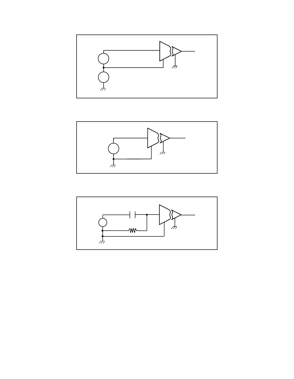
Signal Connections Chapter 3
+
Vs
Vcm
-
Figure 3-2. Ground-Referenced Signal Connection with High Common-Mode Voltage
+
-
Vs
Figure 3-3. Floating Signal Connection Referenced to Chassis Ground for Better SNR
C
c
+
-
Vs
R
b
Figure 3-4. Floating AC-Coupled Signal Connection Referenced
to Chassis Ground for Better SNR
SCXI-1122 User Manual 3-6 © National Instruments Corporation
Page 29
Chapter 3 Signal Connections
C
Vs
Vcm
c
R
b
+
-
Figure 3-5. AC-Coupled Signal Connection with High Common-Mode Voltage
For AC-coupled signals, connect an external resistor from the positive input channel to the signal
reference to provide the DC path for the positive input bias current. Typical resistor values range
from 100 kΩ to 1 MΩ. This solution, although necessary in this case, lowers the input
impedance of the input channel amplifier and introduces an additional offset voltage proportional
to the input bias current and to the resistor value used. The typical input bias current of the
amplifier consists of ±80 pA and a negligible offset drift current. A 100 kΩ bias resistor results
in ±8 µV of offset, which is insignificant in most applications. However, if you use larger
resistors, significant input offset may result. To determine the maximum offset the biasing
resistor will introduce, use the following equation:
V
The input signal range of an SCXI-1122 input channel is ±10 V/ G
input, where G
ofsbias
= I
x R
bias
total
bias
referenced to its negative
total
is equal to the gain selected on the SCXI-1122. In addition, the input channels
are overvoltage protected to 250 Vrms with power on or off at a maximum of 2.5 mArms sink or
source.
Note: The SCXI-1122 input multiplexer is composed of relays. Relays have a certain life
expectancy, as listed in Appendix A, Specifications. To avoid mechanical wear on the
relays, and when you are acquiring a large number of points per channel and
averaging, you should acquire the n samples on a given channel before proceeding to
the next channel. For example, rather than performing 100 scans and taking a single
sample from each channel during each scan, as shown in Figure 3-6a, acquire
100 points on each channel then switch to the next channel and acquire a new set of
samples, as shown in Figure 3-6b.
© National Instruments Corporation 3-7 SCXI-1122 User Manual
Page 30

Signal Connections Chapter 3
Scanned
100
times
average the samples for each channel
a. Bad technique—hardware-driven b. Good technique—software-
scanning wears out relays 100 times driven scanning saves relay life.
faster than the software-driven
scanning.
CH0 (one sample)
CH1 (one sample)
CH2 (one sample)
CH3 (one sample)
100
No
Scans
Done?
Yes
CH0 x 100 samples
CH1 x 100 samples
CH2 x 100 samples
CH3 x 100 samples
average the samples for each channel
Figure 3-6. Avoiding Relay Wear by Sampling and Averaging Rather Than
Single-Sample Channel Scanning
Excitation Channel Signal Connections
Your SCXI-1122 has a voltage (VEX) and a current (IEX) excitation channel, which are
available at the front connector. In addition, VEX/2 is available for half-bridge and quarterbridge transducers. Both channels are isolated from earth ground up to 480 Vrms working
common-mode voltage. Notice that the voltage and current excitations are electrically isolated
from each other but do not provide a safety isolation between them.
Warning: Exceeding the overvoltage protection or isolation rating on the excitation output
can damage the SCXI-1122, the SCXIbus, and the DAQ board. National
Instruments is
NOT liable for any damages or injuries resulting from such signal
connections.
Excitation Level
Each excitation channel of your SCXI-1122 has one level:
• Current excitation–1 mA
• Voltage excitation–3.333 V
It is important that you do not exceed the maximum permissible load of each channel, listed in
Table 3-1.
SCXI-1122 User Manual 3-8 © National Instruments Corporation
Page 31

Chapter 3 Signal Connections
Table 3-1. Maximum Load per Excitation Channel
Excitation Level Maximum Load
3.333 V 225 mA
1 mA 5 kΩ
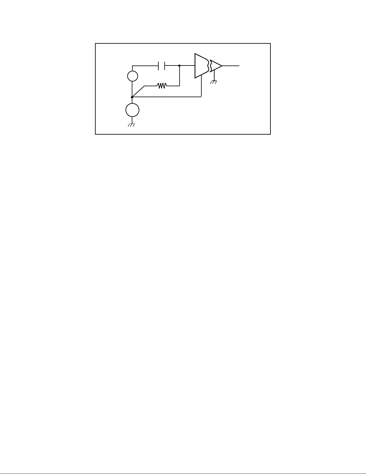
Using the Internal Half-Bridge Completion
Your SCXI-1122 includes half-bridge completion for half-bridge and quarter-bridge setups. The
completion network consists of two 2.5 kΩ ±0.02% ratio tolerance resistors with a temperature
coefficient of
2 ppm/°C. These resistors are connected in series. To use the network, connect
the VEX/2 screw terminal on the terminal block to the negative input of the channel of interest.
VEX+
120 Ω
Strain
Gauge
CH+0
CH-0
120 Ω
Dummy
Resistor
VEX/2
VEX-
SCXI-1322 Terminal Block
Figure 3-7. Connecting a Quarter-Bridge Strain Gauge to Channel 0
Note: When using the half-bridge completion network with a quarter-bridge setup, you must
use an extra resistor to complete the bridge. Place this resistor on the terminal block
between the positive input channel and the negative excitation output.
Temperature Sensor Connection
Pins A1 and A3 are for connecting the isolated temperature sensor located on the SCXI-1322
terminal block for cold-junction compensation (CJC) of thermocouples connected to the
SCXI-1122. The connection is overvoltage-protected to 250 Vrms with power on and off.
Warning: Exceeding the overvoltage protection on the temperature connections can damage
the SCXI-1122, the SCXIbus, and the DAQ board. National Instruments is NOT
liable for any damages resulting from such signal connections.
© National Instruments Corporation 3-9 SCXI-1122 User Manual
Page 32

Signal Connections Chapter 3
Rear Signal Connector
Note: If you are using the SCXI-1122 with a National Instruments DAQ board and cable
assembly, you do not need to read the remainder of this chapter. If you are using the
SCXI-1180 feedthrough panel, the SCXI-1343 rear screw terminal adapter, or the
SCXI-1351 one-slot cable extender with the SCXI-1122, read this section.
Figure 3-8 shows the SCXI-1122 rear signal connector pin assignments.
AOGND
MCH0+
OUTREF
SERDATIN
DAQD*/A
SLOT0SEL*
DIGGND
1 2
3 4
5 6
7 8
9 10
11 12
13 14
15 16
17 18
19 20
21 22
23 24
25 26
27 28
29 30
31 32
33 34
35 36
AOGND
MCH0-
DIGGND
SERDATOUT
SCANCLK
SERCLK
RSVD
37 38
39 40
41 42
43 44
45 46
47 48
49 50
RSVD
Figure 3-8. SCXI-1122 Rear Signal Connector Pin Assignments
SCXI-1122 User Manual 3-10 © National Instruments Corporation
Page 33

Chapter 3 Signal Connections
Rear Signal Connection Descriptions
Pin Signal Name Description
1, 2 AOGND Analog Output Ground–These pins are connected to the
analog reference when jumper W1 is in position AB-R0.
3, 4 MCH0± Analog Output Channels 0–Connects to the DAQ board
differential analog input channels.
19 OUTREF Output Reference–This pin serves as the reference node for
the analog channels output in the pseudodifferential
reference mode. It should be connected to the analog input
sense of the NRSE DAQ board.
24, 33 DIGGND Digital Ground–These pins supply the reference for DAQ
board digital signals and are tied to the module digital
ground.
25 SERDATIN Serial Data In–This signal taps into the SCXIbus MOSI line
to send serial input data to a module or Slot 0.
26 SERDATOUT Serial Data Out–This signal taps into the SCXIbus MISO
line to accept serial output data from a module.
27 DAQD*/A DAQ Board Data/Address Line–This signal taps into the
SCXIbus D*/A line to indicate to the module whether the
incoming serial stream is data or address information.
29 SLOT0SEL* Slot 0 Select–This signal taps into the SCXIbus INTR* line
to indicate whether the information on MOSI is being sent
to a module or Slot 0.
36 SCANCLK Scan Clock–This indicates to the SCXI-1122 that a sample
has been taken by the DAQ board and causes the
SCXI-1122 to change channels.
37 SERCLK Serial Clock–This signal taps into the SCXIbus SPICLK
line to clock the data on the MOSI and MISO lines.
43, 46 RSVD Reserved.
All other pins are not connected.
The signals on the rear signal connector can be classified as analog output signals, digital I/O
signals, or timing I/O signals. Signal connection guidelines for each of these groups are given in
the following section.
Analog Output Signal Connections
Pins 1 through 4 and pin 19 of the rear signal connector are analog output signal pins. Pins 1
and 2 are AOGND signal pins. AOGND is an analog output common signal that is routed
through jumper W1 to the analog reference on the SCXI-1122. You can use these pins as a
general analog power ground tie point to the SCXI-1122 if necessary.
© National Instruments Corporation 3-11 SCXI-1122 User Manual
Page 34

Signal Connections Chapter 3
In particular, when using differential input DAQ boards such as the MIO-16 boards, it is
preferable to leave jumper W1 in its factory setting or in position AB-R1 to avoid ground loops.
With DAQ boards that are configured for referenced single-ended (RSE) measurements, set
jumper W1 in position AB-R0 to connect the SCXI-1122 ground to the DAQ analog ground.
Pin 19 is the OUTREF pin; this pin is connected internally to the analog reference when jumper
W1 is in position AB-R2. Pins 3 and 4 are the analog output channel of the SCXI-1122. Pins 3
and 4 or MCH0± are a multiplexed output of the input channels and the temperature sensor
output. Notice that the temperature sensor is located on the terminal block.
Warning: The SCXI-1122 analog outputs are not overvoltage-protected. Applying external
voltages to these outputs can damage the SCXI-1122. National Instruments is
NOT
liable for any damages resulting from such signal connections.
Note: The SCXI-1122 analog outputs are short-circuit protected.
Digital I/O Signal Connections
Pins 24 through 27, 29, 33, 36, 37, 43, and 46 constitute the digital I/O lines of the rear signal
connector–the digital input signals, the digital output signals, and the digital timing signals.
The digital input signals are pins 24, 25, 27, 29, 33, and 37. The DAQ board uses these pins to
configure an SCXI module that is under DAQ board control. Each digital line emulates the
SCXIbus communication signals as follows:
• Pin 25, SERDATIN, is equivalent to the SCXIbus MOSI serial data input line.
• Pin 27, DAQD*/A, is equivalent to the SCXIbus D*/A line. It indicates to the module
whether the incoming serial stream on SERDATIN is data (DAQD*/A = 0), or address
(DAQD*/A = 1) information.
• Pin 29, SLOT0SEL*, is equivalent to the SCXIbus INTR* line. It indicates whether the data
on the SERDATIN line is being sent to Slot 0 (SLOT0SEL* = 0) or to a module
(SLOT0SEL* = 1).
• Pins 24 and 33 are the digital ground references for the DAQ board digital signals and are
tied to the module digital ground.
• Pin 37, SERCLK, is equivalent to the SCXIbus SPICLK line and is used to clock the serial
data on the SERDATIN line into the module registers.
The digital output signal, pin 26, is SERDATOUT and is equivalent to SCXIbus MISO.
The SCXI-1122 digital input and output signals match the digital I/O lines of the MIO-16 boards.
When used with an SCXI-1341, SCXI-1342, or SCXI-1344 cable assembly, the SCXI-1122
signals match the digital lines of the Lab-NB/PC/PC+, the PC-LPM-16, and the Lab-LC boards,
respectively. Table 3-2 lists the equivalences. For more detailed information, consult your cable
installation guide.
SCXI-1122 User Manual 3-12 © National Instruments Corporation
Page 35

Chapter 3 Signal Connections
Table 3-2. SCXIbus to SCXI-1122 Rear Signal Connector to DAQ Board Pin Equivalences
SCXIbus Line SCXI-1122
MIO-16 Lab Boards PC-LPM-16
Rear Signal
Connector
MOSI SERDATIN ADIO0 PB4 DOUT4
D*/A DAQD*/A ADIO1 PB5 DOUT5
INTR* SLOT0SEL* ADIO2 PB6 DOUT6
SPICLK SERCLK EXTSTROBE* PB7 DOUT7
MISO SERDATOUT BDIO0 PC1 DIN6
The digital timing signals are pins 36, 43, and 46.
• Pin 36 is used as a clock by the SCXI-1122 to increment to the next channel after each
conversion by the DAQ board during scanning. This signal is referred to as SCANCLK.
• Pin 43 is a reserved digital input.
• Pin 46 is a reserved digital input.
The following specifications and ratings apply to the digital I/O lines:
• Absolute maximum voltage input rating 5.5 V with respect to DIGGND
• Digital input specifications (referenced to DIGGND):
-VIH input logic high voltage 2 V minimum
-V
-I
input logic low voltage 0.8 V maximum
IL
input current leakage ±1 µA maximum
I
• Digital output specifications (referenced to DIGGND):
-VOH output logic high voltage 3.7 V minimum at 4 mA maximum
-V
output logic low voltage 0.4 V maximum at 4 mA maximum
OL
© National Instruments Corporation 3-13 SCXI-1122 User Manual
Page 36

Chapter 4 Theory of Operation
This chapter contains a functional overview of the SCXI-1122 module and explains the operation
of each functional unit making up the SCXI-1122.
Functional Overview
The block diagram in Figure 4-1 illustrates the key functional components of the SCXI-1122.
© National Instruments Corporation 4-1 SCXI-1122 User Manual
Page 37

Theory of Operation Chapter 4
MCH0+
+1
and
LPF
Mux
Output
LPF-Sel & Output Control
Gain
LPF-Sel
Gain
LPF
MCH0-
AB0 Switch
AB0 Control
AB0-
AB0+
Rear Signal Connector
SCXIbus Connector
&
Interface
Digital Control
Calibration EEPROM
Gain
VEX+
R
Attenuator
shunt
+
LPF
100:1
and
CH0
Gain
LPF
Protection
Temp+
-
Selector
Amplifier Input
Auto
Zero
8 Input Relays
+
-
CH7
LPF-Sel and
Output Control
AB0
Control
Attenuator
Gain
Amplifier Input
MIEX
Selector Control
LPF-Sel
Amplifier Input Selection Control
IEX-
Mux
Counter
Counter
IEX+
Control
+
Relays
8 InputT/Output
Protection
+
-
+
-
CH8
CH15
TEMP+
Status Register
Configuration Register
Temp
TEMP-
RSVD
Source
Current
IEX-
IEX+
Voltage
VEX+
VEX/2
SENSE+
Source
VEX-
SENSE-
Figure 4-1. SCXI-1122 Block Diagram
SCXI-1122 User Manual 4-2 © National Instruments Corporation
Page 38

Chapter 4 Theory of Operation
The major components of the SCXI-1122 are as follows:
• The rear signal connector
• The SCXIbus connector
• The SCXIbus interface
• The digital control circuitry
• The analog circuitry
The SCXI-1122 consists of 16 isolated multiplexed channels with gains of 0.01, 0.02, 0.05, 0.1,
0.2, 0.5, 1, 2, 5, 10, 20, 50, 100, 200, 500, 1,000, and 2,000, and two isolated excitation channels
with voltage and current excitation. The SCXI-1122 also has a digital section for automatic
control of channel scanning, temperature selection, gain selection, and filter selection.
The remainder of this chapter describes the theory of operation for each of these components.
Rear Signal Connector, SCXIbus Connector, and SCXIbus Interface
The SCXIbus controls the SCXI-1122. The SCXIbus interface interfaces the signals of the rear
signal connector to the SCXIbus, allowing a DAQ board to control the SCXI-1122 and the rest of
the chassis.
Digital Control Circuitry
The digital control section consists of the Address Handler Register, the Configuration Register,
the Status Register, and the Module ID Register. The Address Handler Register controls which
register is being addressed. The Configuration Register configures the SCXI-1122 such as gain
selection, shunt calibration, filter bandwidth, two-wire or four-wire scanning, CJS selection, and
auto-zeroing. The Status Register indicates if the SCXI-1122 is done configuring its internal
circuitry or is still in progress of doing so. The Module ID Register contains the module ID A
hex, a code unique to the SCXI-1122. You can read this module ID over the SCXIbus to
determine the type of module in a particular slot.
Analog Circuitry
The analog circuitry consists of a relay multiplexer, a software-programmable gain isolation
amplifier, software-programmable filtering, a temperature sensor channel for cold-junction
compensation, calibration hardware, and voltage and current excitation channel outputs.
Analog Input Channels
The relay multiplexer feeds into the isolation amplifier. This relay multiplexer can be configured
in two-wire or four-wire mode scanning. In two-wire scan mode all sixteen channels operate as
voltage sense channels. At any point in time one and only one of sixteen channels is connected
to the isolation amplifier. In the four-wire scan mode the sixteen channels are divided into two
© National Instruments Corporation 4-3 SCXI-1122 User Manual
Page 39

Theory of Operation Chapter 4
banks which switch synchronously. The eight upper channels (0 through 7) operate as voltage
sense channels and one out of eight is connected to the amplifier at any given point in time. In
addition, the eight lower channels (8 through 15) operate as current output channels which switch
in tandem with the sense channels. At any given point in time one and only one channel is
connected to the current output channels. Table 4-1 indicates the sense/current output channel
associations.
Table 4-1. Sense/Current Output Channel Associations
Sense Current Output
Channel 0 Channel 8
Channel 1 Channel 9
Channel 2 Channel 10
Channel 3 Channel 11
Channel 4 Channel 12
Channel 5 Channel 13
Channel 6 Channel 14
Channel 7 Channel 15
The temperature sensor consists of a thermistor located on the SCXI-1322 terminal block. This
thermistor connects via the temperature channel to the isolation amplifier. The temperature
sensor is for cold junction compensation of thermocouples. When measuring the temperature
sensor output, set your SCXI-1122 for a gain of five and 4 Hz filter. This will increase the
measurement resolution and accuracy as well as reduce noise.
Note: With a 4 Hz bandwidth you must wait one second before you take the temperature
measurement to permit the system to settle. If you want to use the 4 kHz filter, take a
large number of samples and average them. To achieve 50 or 60 Hz rejection, you
should acquire data over an integral number of power line cycles, then average this
data.
The filtering consists of one of two low pass filters, 4 kHz (-3 dB) or 4 Hz (-10 dB), which you
can select via software control. These filters are cascaded and are located in two stages. This is
done to eliminate noise introduced by the isolation amplifier.
The isolation amplifier fulfills two purposes on the SCXI-1122 module. The isolation amplifier
converts a small signal riding on a high common-mode voltage into a single-ended signal with
respect to the SCXI chassis ground. With this conversion, you can extract the input analog
signal from a high common-mode voltage or noise before it is sampled and converted by the
DAQ board. The isolation amplifier also amplifies and conditions an input signal, which results
in an increase in measurement resolution and accuracy. The isolation amplifier drives the analog
output stage which consists of hardware circuitry which permits several module outputs to
multiplex into one DAQ board channel.
The calibration hardware consists of a software-controlled shunt calibration resistor for strain
gauge calibration, an auto-zero calibration for nulling the amplifier offsets, and of an EEPROM
which holds calibration constants for software correction of gain and offset of the isolation
amplifier and of the current and voltage excitations. Refer to your software user manual
(NI-DAQ, LabVIEW, or LabWindows) for further details and to the Excitation Calibration
section in Chapter 5, Calibration.
SCXI-1122 User Manual 4-4 © National Instruments Corporation
Page 40

Chapter 4 Theory of Operation
Excitation Output Channels
In addition to the isolated input channels, the SCXI-1122 has isolated excitation channels, one
3.333 V voltage output source and one 1 mA current output source. Both–like the relay input
channel–have a 480 Vrms common-mode voltage with respect to earth ground and
250 Vrms common-mode voltage between each other and any other channel. Both channels are
overvoltage protected to 250 Vrms and are current limited. The voltage excitation channel is
provided for transducers, such as strain gauges, which need voltage excitation to operate
properly. The maximum current sourcing that this channel can provide is 225 mA. Exceeding
this limit will cause the channel to lose regulation. This channel has four terminals, two sense
terminals (SENSE+ and SENSE-) and two excitation terminals (VEX+ and VEX-). This is done
to provide remote load regulation. For proper operation, the SENSE+ terminal must always be
connected to the VEX+, and the SENSE- terminal to the VEX-. Refer to the SCXI-1322
Terminal Block Installation Guide for further details on using the sense terminals for remote load
sensing.
One of the primary applications of this channel is to provide power to a strain gauge configured
in a Wheatstone bridge. To permit verification of proper bridge operation, we have provided you
with shunt calibration means. This can be done programmatically.
When you select shunt calibration while you are performing a Wheatstone bridge strain
measurement , a 301 kΩ 1% resistor internally shunts across the strain gauge between the VEX+
and the CH+; this resistor is socketed to permit you to change its value to meet your
requirements. If you are performing several strain measurements, you can enable the shunt
calibration then proceed with scanning all of the channels of interest. When you have completed
your check, you can disable the shunt calibration and proceed with your measurement. Notice
that when you are either enabling or disabling the shunt calibration resistor, you must wait 1 s if
you have selected 4 Hz bandwidth or 10 ms if you have selected 4 kHz bandwidth before making
your measurement to permit the system to settle. Finally, to determine the effect of the shunt
resistor on your measurement, follow the procedure below.
Assuming a quarter-bridge strain-gauge configuration with a gauge factor of GF = 2, the
equivalent strain change the R
shunting resistor introduces is -199 µε. This is determined as
SCAL
follows:
1. Determine the change the shunting resistor causes using the following formula:
V
change
=
VexR(R
R
SCAL
SCAL+Rg
+R(R
SCAL+Rg
)
)
−
V
ex
2
2. Using the appropriate strain-gauge strain formula, and assuming that you have no static
voltage, determine the equivalent strain that the R
if your SCXI system is configured with R
with a gauge factor of GF = 2, V
V
= 0.3321 mV
change
Replacing the strained voltage with V
= 3.333 V, and R = 120 Ω, the following result occurs:
EX
change
= 301 kΩ, a quarter-bridge 120 Ω strain gauge
SCAL
in the quarter-bridge strain equation produces an
resistor should produce. For example,
SCAL
equivalent -199 µε of change.
Also, the module has an internal completion network that you can use with half-bridge or
quarter-bridge networks. To use this completion network, simply connect the VEX/2 terminal to
the negative input channel of the appropriate transducer channel. In case of a quarter-bridge
configuration, you must provide an additional resistor–equal in value to your nominal strain
© National Instruments Corporation 4-5 SCXI-1122 User Manual
Page 41

Theory of Operation Chapter 4
gauge resistor–to complete the bridge network. Connect this resistor in your SCXI-1322
terminal block between the CH+ and VEX- terminals.
The current output channel is provided for transducers–such as thermistors and RTDs–which
need a current excitation to operate properly. The current output has a value of 1 mA and has a
maximum permissible load of 5 kΩ. If you connect loads greater than 5 kΩ, the current source
will lose regulation. When connecting several loads which need current excitation, you have two
possible approaches. The first is to connect them all in series (as long as they do not exceed
5 kΩ total) and use the two-wire scan mode as shown in Figure 4-2 or use the four-wire scan
mode and have them connected as shown in Figure 4-3.
R
1
R
2
R
3
R
15
CH+0
CH-0
CH+1
CH-1
CH+2
CH-2
CH+15
CH-15
RT = R1 +...+R15 ≤ 5 kΩ
IEX+
IEX-
Figure 4-2. Series Connection with Current Excitation
CH+8
R
1
CH+0
CH-0
CH-8
CH+9
R
2
R
3
Any R ≤ 5 kΩ
CH+1
CH-1
CH-9
CH+15
CH+7
CH-7
CH-15
Figure 4-3. Four-Wire Scan Connection with Multiplexed Current Excitation
SCXI-1122 User Manual 4-6 © National Instruments Corporation
Page 42

Chapter 4 Theory of Operation
Note: Always connect the current excitation terminals outside the sense terminals as shown
in both Figures 4-2 and 4-3.
Each approach has its advantages and disadvantages as listed in Table 4-2.
Table 4-2. Pros and Cons of Two-Wire and Four-Wire Connections
with Current Excited Transducers
Type Pros Cons
Series connection with
two-wire scanning
Independent connection
with four-wire scanning
16 transducers per module
All transducers are
continuously excited
Two-wire connections are
easier to connect because of
fewer wires
5 kΩ per channel
250 Vrms CMV between
transducers
Limited to 5 kΩ total
resistance
No isolation between
channels
Eight transducers maximum
per module
More connections
© National Instruments Corporation 4-7 SCXI-1122 User Manual
Page 43

Chapter 5 Calibration
This chapter discusses the calibration procedures for the SCXI-1122.
Overview
The onboard calibration hardware that calibrates the SCXI-1122, consists of an EEPROM to
store the calibration constants and an auto-zero channel on the amplifier input selector. When
the auto-zero channel is selected, the input relay multiplexer is disconnected from the amplifier
inputs and the isolation amplifier inputs are connected to its ground reference.
Auto-zeroing is a method for nulling error sources that compromise the quality of measurements.
Auto-zeroing determines the amount of offset at the output of the SCXI-1122 at a given gain of
the amplifier. It is recommended to perform auto-zeroing at the start of an experiment for each
gain to be used to eliminate error due to drift in the amplifier internal circuitry and increase the
accuracy of the measurement. Notice that the auto-zero path is different from the analog input
path; therefore, even after auto-zeroing, a residual input offset still exists and has a value of less
than 6 µV. Refer to Appendix A, Specifications, for further details.
You can store this offset in the onboard EEPROM for future use and for automatic calibration
when you are using National Instruments software. The EEPROM also stores correction factors
for each gain of the SCXI-1122 as well as for the excitation channels. If you are not using
National Instruments software, refer to the SCXI-1122 Register-Level Programmer Manual if
you need a more a detailed description of the EEPROM.
When using National Instruments software such as NI-DAQ, LabVIEW, and LabWindows, and
you are using the factory-determined calibration constants, you do not need to read the following
section; continue reading the Excitation Calibration section. You need to read the following
section only if you are using National Instruments software and you intend to determine new
calibration constants.
Calibration Procedure
Calibration Equipment Requirements
According to standard practice, the equipment used to calibrate the SCXI-1122 should be 10
times as accurate as the SCXI-1122. Practically speaking, calibration equipment with four times
the accuracy of the item under calibration is generally considered acceptable. To calibrate the
SCXI-1122, you need the following equipment.
• For the amplifier gains, you need a voltmeter with the following specifications:
- Accuracy ±0.002% standard
±0.08% sufficient
- Range -10 to +10 V
© National Instruments Corporation 5-1 SCXI-1122 User Manual
Page 44

Calibration Chapter 5
- Resolution 8 1/2 digits
• For the excitation channels, you need a voltmeter with the following specifications:
- Accuracy ±0.004% standard
±0.16% sufficient
- Range 0 to +5 V
- Resolution 5 1/2 digits
• You need an ammeter with the following specifications:
- Accuracy ±0.004% standard
±0.16% sufficient
- Range 1 mA
- Resolution 6 1/2 digits
A multiranging 8 1/2-digit digital multimeter can perform all of the necessary functions
previously described. In the rest of this section, the measuring instrument is referred to as a
digital multimeter (DMM).
To make sure that the DMM does not introduce an additional offset, you can determine the offset
errors of the DMM by shorting its leads together and reading the measured value. This value, the
DMM offset, must be subtracted from all subsequent measurements.
Gain and Offset Calibration
To determine the offset and gain calibration factors of the SCXI-1122 at a given gain, Gs,
perform the following steps for a two-point calibration.
1. Set the SCXI-1122 to the desired gain.
2. Depending on how you want to calibrate your module, you can perform one of the following
procedures.
• Auto-zeroing selects one of the calibration points to be at 0 V input and you must provide
the other calibration point at positive or negative full scale:
a. Enable auto-zeroing.
b. Measure the SCXI-1122 output with the DMM and store the measured value for
future use.
c. Disable auto-zeroing.
d. Apply 9.9 V/Gs or -9.9 V/Gs to the amplifier input.
e. Go to step 3.
SCXI-1122 User Manual 5-2 © National Instruments Corporation
Page 45

Chapter 5 Calibration
• To select positive and negative full scale to be the two calibration points, apply -9.9 V/G
s
and 9.9 V/Gs..
a. Apply -9.9 V/Gs to the amplifier input.
b. Measure the input voltage with the DMM and store the measured value.
c. Measure the SCXI-1122 output with the DMM and store the measured value.
d. Apply 9.9 V/Gs at the amplifier input.
e. Go to step 3.
Note: If you are using a calibrator that supplies accurate voltages, you can skip step c directly
above and step 3 below.
3. Measure the input voltage with the DMM and the store the measured value.
4. Measure the SCXI-1122 output with the DMM and store the measured value.
5. You now have two pairs of voltages. Each pair consists of an input voltage and an output
voltage. For the autozeroing option, the pairs are {0 V input, offset output} and
{9.9 V/Gs input, 9.9 V output} or {-9.9 V/Gs input, -9.9 V output}. For the positive or
negative full-scale calibration points option, the pairs are {-9.9 V/Gs input, -9.9 V output}
and {9.9 V/Gs input, 9.9 V output}.
6. Convert the output voltage from volt units to your DAQ board binary unit. You must take
into consideration the polarity of your DAQ board, its resolution (12 bits or 16 bits), and
gain. For example, if you are using an AT-MIO-16F-5 in bipolar mode and are using a gain
of G
= 0.5, your output voltages for the autozeroing option will be represented in binary
MIO
units as given by the following formula:
12
Binary = Voltage •
2
• G
MIO
10
Refer to your DAQ board user manual to determine the appropriate formula for you to use.
7. You now have a new set of pairs referred to as voltage binary pairs {V input1, Binary
output1} and {V input2, Binary output2}. Pass these pairs to the SCXI_Cal_Constants
function or VI as described in your software user manual.
Notes: When you are using the autozeroing option with 0 V and 9.9 V/G
, this sets your gain
s
error to 0% at 0 V and at positive full-scale voltage. However, because of nonlinearity,
the error at the negative full-scale voltage will be two times the nonlinearity error. This
is also true for the positive full-scale voltage if you use the negative full-scale voltage
and 0 V as your two calibration points.
When you are making a measurement and using National Instruments software, the
driver automatically performs the software correction.
© National Instruments Corporation 5-3 SCXI-1122 User Manual
Page 46

Calibration Chapter 5
Excitation Calibration
When using the excitation channels, you must retrieve the correction factors for the current and
voltage from the EEPROM before using them in your transducer conversion formulas. Refer to
your software user manual for how to use the SCXI_Cal_Constants function or VI to
perform this task.
You do not need to read the following section if you are going to use the factory-determined
correction factors and you are using National Instruments software.
If you want to determine a new set of voltage excitation calibration constants and you are using
National Instruments software, use the following procedure:
1. Connect a 15 Ω resistor to the excitation channel.
2. Connect the DMM across the 15 Ω load and measure the voltage.
3. Pass this voltage to the SCXI_Cal_Constants function or VI.
To determine the current excitation calibration constants, follow this procedure:
1. Set your DMM to DC current measurements.
2. Connect the DMM across the IEX+ and IEX- terminals and measure the current.
3. Pass this current to the SCXI_Cal_Constants function or VI.
Note: When calibrating your system, you must verify that your offsets, gain errors, and
excitation errors do not exceed the ranges listed in Table 5-1.
Table 5-1. Maximum Allowable Error Ranges
Error Type Error Range
All gains ±2%
Offset at G = 0.01 ±40 mV
Offset at G = 0.02 ±40 mV
Offset at G = 0.05 ±50 mV
Offset at G = 0.1 ±50 mV
Offset at G = 0.2 ±50 mV
Offset at G = 0.5 ±50 mV
Offset at G = 1 ±40 mV
Offset at G = 2 ±40 mV
Offset at G = 5 ±50 mV
Offset at G = 10 ±50 mV
Offset at G = 20 ±50 mV
Offset at G = 50 ±50 mV
Offset at G = 100 ±60 mV
Offset at G = 200 ±70 mV
Offset at G = 500 ±100 mV
Offset at G = 1,000 ±200 mV
Offset at G = 2,000 ±400 mV
Current excitation ±3%
Voltage excitation ±1%
SCXI-1122 User Manual 5-4 © National Instruments Corporation
Page 47

Appendix A Specifications
This appendix lists the specifications for the SCXI-1122. These are typical at 25° C unless
otherwise stated.
Analog Input
Input Characteristics
Number of channels 16 differential, 8 4-wire, software selectable
Input signal ranges
Module Gain Max
Module Range
1
(Software Selectable)
0.01 ±250 VDC or Vrms
0.02 ±250 V
0.05 ±200 V
0.1 ±100 V
0.2 ±50 V
0.5 ±20 V
1 ±10 V
2 ±5 V
5 ±2 V
10 ±1 V
20 ±500 mV
50 ±200 mV
100 ±100 mV
200 ±50 mV
500 ±20 mV
1,000 ±10 mV
2,000 ±5 mV
Input coupling DC
Max working voltage Each input should remain within 480
(signal + common mode) ground, and within 250 Vrms of any other channel
Overvoltage protection 250 Vrms powered on, 250 V powered off
Protected terminals CH < 0..15 >, IEX+, IEX-, VEX+, VEX-
±10 V
Vrms of
1
Vrms refers to sinusoidal waveform; V refers to DC or AC peak.
© National Instruments Corporation A-1 SCXI-1122 User Manual
Page 48

Specifications Appendix A
Transfer Characteristics
Nonlinearity 0.01% FSR
Offset error
Gain ≥ 1 ±(6 µV + 1,240 µV/gain)
Gain < 1 ±(352 µV + 1,240 µV/gain)
Gain error
Gain ≥ 1 ±0.02% of reading
Gain < 1 ±0.10% of reading
Amplifier Characteristics
Input impedance
Normal powered on 1 GΩ in parallel with 100 pF for gain ≥ 1,
1 MΩ in parallel with 100 pF for gain < 1
Powered off 100 kΩ
Overload 100 kΩ
Input bias current ±80 pA
CMRR
Filter Bandwidth CMRR 50 or 60 Hz
4 Hz 160 dB
4 kHz 100 dB
Output range ±10 V
Output impedance 75 Ω
Dynamic Characteristics
Bandwidth (-3 dB) 4 Hz (-10 dB) or 4 kHz, software selectable
Settling time to full-scale step (all gains)
with 4 kHz filter enabled 10 ms
with 4 kHz filter enabled 1 s
System noise
Gain 4 Hz Filter 4 kHz Filter
1 150 µVrms 1 mVrms
1,000 1,000 nVrms 4 µVrms
Slew rate 0.10 V/µs
Filters
Type 3-pole RC
Cutoff frequency (-3 dB) 4 Hz (-10 dB) or 4 kHz, software selectable
NMR (50 or 60 Hz) 60 dB at 4 Hz bandwidth
Stability
Recommended warm-up time 20 minutes
Offset temperature coefficient ±(0.2 + 150/gain) µV/°C
Gain temperature coefficient ±10 ppm/°C for gain ≥ 1, ± 25 ppm/°C for gain < 1
SCXI-1122 User Manual A-2 © National Instruments Corporation
Page 49

Appendix A Specifications
Excitation
Output Characteristics
Channels 2 (1 voltage and 1 current)
Bridge type Quarter, half, or full
Bridge completion Two 2.5 kΩ ±0.02% ratio tolerance resistors
Voltage Mode
Level 3.333 V ±0.04%
Current drive 225 mA
Drift 30 ppm/°C
Current Mode
Level 1.0 mA ±0.04%
Max load resistance 5 kΩ
Drift 40 ppm/°C
Physical
Dimensions 3.0 by 17.3 by 20.3 cm (1.2 by 6.8 by 8.0 in.)
I/O connectors 50-pin male ribbon cable rear connector
48-pin male DIN C front I/O connector
Environment
Operating temperature 0 to 50 ° C
Storage temperature -20 to 70 C
Relative humidity 10% to 90%
Maximum altitude <2000 meters
°
Safety
Electrical Measuring and IEC/EN 61010-1, UL 3111-1,
Test Equipment CAN/CSA C22.2, No. 1010.1
Installation Category Category II
Pollution degree 2
© National Instruments Corporation A-3 SCXI-1122 User Manual
Page 50

Appendix B Customer Communication
For your convenience, this appendix contains forms to help you gather the information necessary
to help us solve technical problems you might have as well as a form you can use to comment on
the product documentation. Filling out a copy of the Technical Support Form before contacting
National Instruments helps us help you better and faster.
National Instruments provides comprehensive technical assistance around the world. In the U.S.
and Canada, applications engineers are available Monday through Friday from 8:00 a.m. to
6:00 p.m. (central time). In other countries, contact the nearest branch office. You may fax
questions to us at any time.
Corporate Headquarters
(512) 795-8248
Branch Offices Phone Number
Australia 03 9879 5166
Austria 0662 45 79 90 0
Belgium 02 757 00 20
Brazil 011 284 5011
Canada (Calgary) 403 274 9391
Canada (Ontario) 905 785 0085
Canada (Québec) 514 694 8521
China 0755 3904939
Denmark 45 76 26 00
Finland 90 725 725 11
France 1 48 14 24 24
Germany 089 741 31 30
Greece 30 1 42 96 427
Hong Kong 2645 3186
India 91805275406
Israel 03 6120092
Italy 02 413091
Japan 03 5472 2970
Korea 02 596 7456
Mexico (D.F.) 5 280 7625
Mexico (Monterrey) 8 357 7695
Netherlands 0348 433466
Norway 32 27 73 00
Singapore 2265886
Spain (Barcelona) 93 582 0251
Spain (Madrid) 91 640 0085
Sweden 08 587 895 00
Switzerland 056 200 51 51
Taiwan 02 2377 1200
U.K. 0635 523545
© National Instruments Corporation B-1 SCXI-1122 User Manual
Page 51

Technical Support Form
___________________________________________________
Photocopy this form and update it each time you make changes to your software or hardware, and use the completed
copy of this form as a reference for your current configuration. Completing this form accurately before contacting
National Instruments for technical support helps our applications engineers answer your questions more efficiently.
If you are using any National Instruments hardware or software products related to this problem, include the
configuration forms from their user manuals. Include additional pages if necessary.
Name
Company
Address
Fax ( ) Phone ( )
Computer brand Model Processor
Operating system
Speed MHz RAM MB Display adapter
Mouse yes no Other adapters installed
Hard disk capacity MB Brand
Instruments used
National Instruments hardware product model Revision
Configuration
National Instruments software product Version
Configuration
The problem is
List any error messages
The following steps will reproduce the problem
Page 52

SCXI-1122 Hardware Configuration Form
Record the settings and revisions of your hardware and software on the line to the right of each item. Complete a
new copy of this form each time you revise your software or hardware configuration, and use this form as a
reference for your current configuration. Completing this form accurately before contacting National Instruments
for technical support helps our applications engineers answer your questions more efficiently.
• SCXI-1122 Revision Letter _____________________________________________________
• Chassis Slot _____________________________________________________
• Grounding, Shielding, and Reference
Mode Selection (Factory Setting:
Parking position, W1, A-R0R1) _____________________________________________________
• SERDATOUT Resistor Pull-up Jumper
(Factory Setting: Enabled, W2, position 1) _____________________________________________________
• Other Modules in System _____________________________________________________
_____________________________________________________
• DAQ Boards Installed _____________________________________________________
_____________________________________________________
Page 53

Register-Level Programmer Manual Request Form
National Instruments encourages you to comment on the documentation supplied with our products. This
information helps us provide quality products to meet your needs.
Title: SCXI-1122 Register-Level Programmer Manual
Part Number: 340696-01
Please indicate your reasons for obtaining the register-level programmer manual. Check all that apply.
National Instruments does not support your operating system or programming language.
You are an experienced register-level programmer who is more comfortable writing your own register-level
software.
Other. Please explain.
Thank you for your help.
Name
Title
Company
Shipping Address
(Street Address, Not P.O. Box)
Phone ( )
Mail to: Customer Service Department Fax to: Customer Service Department
National Instruments Corporation National Instruments Corporation
6504 Bridge Point Parkway (512) 794-5794
Austin, TX 78730-5039
Page 54

Documentation Comment Form
National Instruments encourages you to comment on the documentation supplied with our products. This
information helps us provide quality products to meet your needs.
Title: SCXI-1122 User Manual
Edition Date: September 1999
Part Number: 320516B-01
Please comment on the completeness, clarity, and organization of the manual.
If you find errors in the manual, please record the page numbers and describe the errors.
Thank you for your help.
Name
Title
Company
Address
Phone ( )
Mail to: Technical Publications Fax to: Technical Publications
National Instruments Corporation National Instruments Corporation
11500 N Mopac Expwy (512) 433-8641
Austin, TX 78759-3504
Page 55

Glossary
Prefix Meaning Value
p- picon- nanoµ- micro-
m- millik- kiloM- mega-
Numbers/Symbols
˚ degrees
ε strain
> greater than
≥ greater than or equal to
< less than
- negative of, or minus
Ω ohms
% percent
± plus or minus
+ positive of, or plus
+5 V (signal) +5 VDC Isolated Source signal
10
10
10
10
10
10
-12
-9
-6
-3
3
6
A
A amperes
AC alternating current
A/D analog-to-digital
ADIO# Port A Digital Input/Output signal (0 ≤ # ≤ 5)
ANSI American National Standards Institute
AOGND Analog Output Ground signal
Arms amperes, root mean square
AWG American Wire Gauge
B
BDIO Port B Digital Input/Output signal
C
C Celsius
C
c AC coupling capacitor
© National Instruments Corporation Glossary-1 SCXI-1122 User Manual
Page 56

Glossary
CH#+ Positive Input Channel Number signal
CH#- Negative Input Channel Number signal
CJC cold-junction compensation
CJR cold-junction reference
CJS cold junction sensor
CMRR common-mode rejection ratio
CMV common-mode voltage
D
D/A digital-to-analog
DAQD*/A Data Acquisition Board Data/Address Line signal
dB decibels
DC direct current
DIGGND Digital Ground signal
DIN Deutsche Industrie Norme
DOUT# Data Out Number signal
E
EEPROM electrically erased programmable read-only memory
F
F Farads
FSR full-scale range
G
GF gauge factor
G
G
G
MIO
s
total
MIO gain
SCXI gain
total gain
H
Hz hertz
I
I
bias bias current
IEX current excitation channel
IEX- Negative Current Excitation Output signal
IEX+ Positive Current Excitation Output signal
I
I
input current leakage
in. inches
SCXI-1122 User Manual Glossary-2 © National Instruments Corporation
Page 57

INTR* Interrupt signal
I/O input/output
M
m meters
MB megabytes of memory
MCH#+ Positive Analog Output Channel Number signal
MCH#- Negative Analog Output Channel Number signal
min minutes
MIO multifunction I/O
MISO Master-In-Slave-Out signal
MOSI Master-Out-Slave-In signal
N
NMR normal mode rejection
NRSE nonreferenced single-ended (input)
Glossary
O
OUTREF Output Reference signal
P
ppm parts per million
R
R resistor
RAM random-access memory
R
b
R
bias
RC resistor-capacitor filter
R
g
R
SCAL
RSE referenced single-ended (input)
RSVD Reserved bit/signal
RTD resistance temperature detector
RTSI Real-Time System Integration
bias resistor
bias resistor
strain gauge nominal resistance
shunt resistor
S
SCANCLK Scan Clock signal
SCXI Signal Conditioning eXtensions for Instrumentation (bus)
SDK Software Developer's Kit
© National Instruments Corporation Glossary-3 SCXI-1122 User Manual
Page 58

Glossary
s seconds
SENSE- Negative Voltage Sense signal
SENSE+ Positive Voltage Sense signal
SERCLK Serial Clock signal
SERDATIN Serial Data In signal
SERDATOUT Serial Data Out signal
SLOT0SEL* Slot 0 Select signal
SNR signal-to-noise ratio
SPICLK Serial Peripheral Interface Clock signal
T
TEMP- Temperature Sensor Reference signal
TEMP+ Temperature Sensor Output signal
V
V volts
V
cm
VDC volts direct current
VEX Voltage Excitation Channel signal
VEX- Negative Voltage Excitation Output signal
VEX+ Positive Voltage Excitation Output signal
VEX/2 Half Voltage Excitation Output signal
VI Virtual Instrument
V
IH
V
IL
V
ofsbias
V
OH
V
OL
Vrms volts, root mean square
common-mode voltage
input logic high voltage
input logic low voltage
offset bias voltage
output logic high voltage
output logic low voltage
W
W watts
SCXI-1122 User Manual Glossary-4 © National Instruments Corporation
Page 59

Index
Numbers
+5 V signal, 3-4
A
AC-coupled signal connection with high
common-mode voltage (illustration), 3-7
Address Handler Register, 4-3
analog circuitry, 4-3 to 4-7
analog input channels, 4-3
excitation output channels, 4-3 to 4-7
analog configuration, 2-3 to 2-5
current-loop receivers, 2-4 to 2-5
jumper settings (table), 2-4
analog input channel signal connections, 3-5
to 3-8
AC-coupled signal connection with high
common-mode voltage
(illustration), 3-7
connecting external resistors, 3-7
floating AC-coupled signal connection
referenced to chassis ground
(illustration), 3-6
floating signal connection referenced to
chassis ground (illustration), 3-6
ground-referenced signal connection
with high common-mode voltage
(illustration), 3-6
analog input channels
sense/current output channel associations
(illustration), 4-4
specifications, A-1 to A-3
theory of operation, 4-3 to 4-4
analog output signal connections, 3-11
to 3-12
AOGND signal, 3-11
C
cables
custom cables, 1-5
optional equipment (table), 1-4
calibration
equipment requirements, 5-1 to 5-2
excitation calibration, 4-4, 5-4
gain and offset calibration, 5-2 to 5-3
overview, 5-1
CH-(0:15) signal, 3-4
CH+(0:15) signal, 3-4
configuration. See also installation.
analog configuration, 2-3 to 2-5
current-loop receivers, 2-4 to 2-5
digital signal connections, 2-3
jumper settings
analog configuration, 2-4
digital signal connections, 2-3
parts locator diagram, 2-2
Configuration Register, 4-3
current (IEX) excitation channel, 3-8
current-loop receivers, 2-4 to 2-5
installing
procedure for, 2-5
shock hazard related to, 2-5
user-defined current receiver resistors
(table), 2-4 to 2-5
custom cables, 1-5
customer communication, xii, B-1
D
DAQD*/A signal, 3-11, 3-12
DIGGND signal, 3-11, 3-13
digital control circuitry, 4-3
digital I/O signal connections, 3-12 to 3-13
configuration, 2-3
digital timing signals, 3-13
emulation of SCXIbus communication
signals, 3-12
SCXIbus to SCXI-1122 rear signal
connector to DAQ board pin
equivalences (table), 3-13
specifications and ratings, 3-13
documentation
conventions used, x
National Instruments documentation
set, xi
organization of manual, ix
related documentation, xi
© National Instruments Corporation Index-1 SCXI-1122 User Manual
Page 60

Index
E
EEPROM, 5-1
environment specifications, A-3
equipment, optional, 1-4 to 1-5
excitation channel signal connections, 3-8
to 3-9
connecting quarter-bridge strain gauge to
channel 0 (illustration), 3-9
exceeding overvoltage protection, 3-8
excitation level, 3-8 to 3-9
internal half-bridge completion, 3-9
maximum load per excitation channel
(table), 3-9
excitation output channels
calibration, 4-4, 5-5
four-wire scan connection with
multiplexed current excitation
(illustration), 4-6
pros and cons of two-wire and four-wire
connections with current excited
transducers (illustration), 4-7
series connection with current excitation
(illustration), 4-6
specifications, A-3
theory of operation, 4-3 to 4-7
F
filtering, 4-4
floating AC-coupled signal connection
referenced to chassis ground for better
SNR (illustration), 3-6
floating signal connection referenced to
chassis ground for better SNR
(illustration), 3-6
front connector
AC-coupled signal connection with high
common-mode voltage
(illustration), 3-7
analog input channel signal connections,
3-5 to 3-8
avoiding relay wear (illustration), 3-8
excitation channel signal connections,
3-8 to 3-9
floating AC-coupled signal connection
referenced to chassis ground for better
SNR (illustration), 3-6
floating signal connection referenced to
chassis ground for better SNR
(illustration), 3-6
ground-referenced signal connection
with high common-mode voltage
(illustration), 3-6
pin assignments (illustration), 3-3
signal connection descriptions, 3-4
to 3-5
temperature sensor connection, 3-9
G
gain and offset calibration, 5-2 to 5-3
ground-referenced signal connection with
high common-mode voltage
(illustration), 3-6
H
half-bridge completion network, 3-9, 4-5
hardware installation. See installation.
I
IEX- signal, 3-4
IEX+ signal, 3-4
installation. See also configuration.
current-loop receivers (resistors), 2-4
to 2-5
hardware installation, 2-6
unpacking the SCXI-1122, 1-5
internal half-bridge completion, 3-9, 4-5
isolation amplifier, 4-4
J
jumper settings
analog configuration (table), 2-4
digital signal connections (table), 2-3
L
Lab-NB/PC/PC+ boards
SCXIbus to SCXI-1122 rear signal
connector to DAQ board pin
equivalences (table), 3-13
LabVIEW applications software, 1-2, 2-6
LabWindows applications software, 1-2, 2-6
SCXI-1122 User Manual Index-2 © National Instruments Corporation
Page 61

Index
M
manual. See documentation.
MCH0± signal, 3-11, 3-12
MIO-16 boards
SCXIbus to SCXI-1122 rear signal
connector to DAQ board pin
equivalences (table), 3-13
MISO line, 2-3
module configuration. See configuration.
Module ID Register, 2-3, 4-3
N
NI-DAQ driver software, 1-2 to 1-3, 2-6
noise immunity, 3-5
O
open-collector driver, 2-3
operation of SCXI-1122. See theory of
operation.
optional equipment, 1-4 to 1-5
OUTREF signal, 3-11, 3-12
P
parts locator diagram, 2-2
PC-LPM-16 board
SCXIbus to SCXI-1122 rear signal
connector to DAQ board pin
equivalences (table), 3-13
physical specifications, A-3
pin assignments
front connector (illustration), 3-3
rear signal connector (illustration), 3-10
pin equivalences,
SCXIbus to SCXI-1122 rear signal
connector to DAQ board (table), 3-13
R
rear signal connector
analog output signal connections, 3-11
to 3-12
digital I/O signal connections, 3-12
to 3-13
pin assignments (illustration), 3-10
SCXIbus interface, 4-3
SCXIbus to SCXI-1122 rear signal
connector to DAQ board pin
equivalences (table), 3-13
signal descriptions, 3-11
register-level programming, 1-4
registers
Address Handler Register, 4-3
Configuration Register, 4-3
Module ID Register, 2-3, 4-3
Status Register, 2-3, 4-3
relays
avoiding mechanical wear, 3-7 to 3-8
illustration, 3-8
life expectancy, 3-7
resistors. See current-loop receivers.
S
SCANCLK signal, 3-11, 3-13
SCXI-1122
block diagram, 4-2
features, 1-1
kit contents, 1-1
major components, 4-3
optional equipment, 1-4 to 1-5
purpose, 1-1
software programming choices, 1-2 to 4
unpacking, 1-5
SCXIbus connector, 4-3
SCXIbus interface, 4-3
SCXIbus to SCXI-1122 rear signal
connector to DAQ board pin equivalences
(table), 3-13
SENSE- signal, 3-4, 4-5
SENSE+ signal, 3-4, 4-5
SERCLK signal, 3-11, 3-12
SERDATIN signal, 3-11, 3-12
SERDATOUT signal, 2-3, 3-11, 3-12
signal connections
digital signal connections, 2-3
front connector
AC-coupled signal connection with
high common-mode voltage
(illustration), 3-7
analog input channel signal
connections, 3-5 to 3-8
avoiding relay wear (illustration), 3-8
excitation channel signal
connections, 3-8 to 3-9
floating AC-coupled signal
connection referenced to chassis
© National Instruments Corporation Index-3 SCXI-1122 User Manual
Page 62

Index
ground for better SNR
(illustration), 3-6
floating signal connection referenced
to chassis ground for better SNR
(illustration), 3-6
ground-referenced signal connection
with high common-mode voltage
(illustration), 3-6
pin assignments (illustration), 3-3
signal connection descriptions, 3-4
to 3-5
temperature sensor connection, 3-9
rear signal connector
analog output signal connections,
3-11 to 3-12
digital I/O signal connections, 3-12
to 3-13
pin assignments (illustration), 3-10
SCXIbus to SCXI-1122 rear signal
connector to DAQ board pin
equivalences (table), 3-13
signal descriptions, 3-11
safety warnings, 3-1 to 3-2
SLOT0SEL* signal, 3-11, 3-12
software programming choices
LabVIEW applications software, 1-2
LabWindows applications software, 1-2
NI-DAQ driver software, 1-2 to 1-3
register-level programming, 1-4
specifications
analog input, A-1 to A-3
environment, A-3
excitation, A-3
physical, A-3
Status Register, 2-3, 4-3
U
unpacking the SCXI-1122, 1-5
user-defined current receiver resistors. See
current-loop receivers.
V
VEX- signal, 3-4, 4-5
VEX/2 signal, 3-4
VEX+ signal, 3-4, 4-5
voltage (VEX) excitation channel, 3-8
W
Wheatstone bridge, 4-5
T
TEMP- signal, 3-4, 3-5
TEMP+ signal, 3-4, 3-5
temperature sensor connection, 3-9, 4-4
theory of operation
analog circuitry, 4-3 to 4-7
analog input channels, 4-3
excitation output channels, 4-3 to 4-7
digital control circuitry, 4-3
functional overview, 4-1 to 4-2
major components of SCXI-1122, 4-3
rear signal connector, 4-3
SCXI-1122 block diagram, 4-2
SCXIbus connector, 4-3
SCXIbus interface, 4-3
SCXI-1122 User Manual Index-4 © National Instruments Corporation
 Loading...