

Page 1

™
SCXI
SCXI-1121 User Manual
Four-Channel Isolated Universal Transducer Module
for Signal Conditioning
SCXI-1121 User Manual
September 1999 Edition
Part Number 320426C-01
Page 2

Worldwide Technical Support and Product Information
www.natinst.com
National Instruments Corporate Headquarters
11500 North Mopac Expressway Austin, Texas 78759-3504 USA Tel: 512 794 0100
Worldwide Offices
Australia 03 9879 5166, Austria 0662 45 79 90 0, Belgium 02 757 00 20, Brazil 011 284 5011,
Canada (Calgary) 403 274 9391, Canada (Ontario) 905 785 0085, Canada (Québec) 514 694 8521,
China 0755 3904939, Denmark 45 76 26 00, Finland 09 725 725 11, France 01 48 14 24 24,
Germany 089 741 31 30, Greece 30 1 42 96 427, Hong Kong 2645 3186, India 91805275406,
Israel 03 6120092, Italy 02 413091, Japan 03 5472 2970, Korea 02 596 7456, Mexico (D.F.) 5 280 7625,
Mexico (Monterrey) 8 357 7695, Netherlands 0348 433466, Norway 32 27 73 00, Singapore 2265886,
Spain (Barcelona) 93 582 0251, Spain (Madrid) 91 640 0085, Sweden 08 587 895 00,
Switzerland 056 200 51 51, Taiwan 02 2377 1200, United Kingdom 01635 523545
For further support information, see the Technical Support Resources appendix. To comment on the
documentation, send e-mail to techpubs@natinst.com.
© Copyright 1992, 1999 National Instruments Corporation. All rights reserved.
Page 3

Important Information
Warranty
The SCXI-1121 is warranted against defects in materials and workmanship f or a period of one year from the date of shipment,
as evidenced by receipts or other documentation. National Instruments will, at its option, repair or replace equipment that
proves to be defective during the warranty period. T his w arran ty i ncludes part s and l abo r.
A Return Material Authorization (RMA) number must be obtained from the factory and clearly marked on the outside of
the package before any equipment will be accepted for warranty work. National Instruments will pay the shipping costs of
returning to the owner parts which are covered by warrant y.
National Instruments believes that the information in this document is accurate. The document has been carefully reviewed
for technical accuracy. In the event that technical or typographical errors exist, National Instruments reserves the right to
make changes to subsequent editions of this document without prior notice to holders of this edition. The reader should consult
National Instruments if errors are suspected. In no even t shall Nati on al Inst rum ents be l iable fo r any dama ges aris in g o ut of
or related to this document or the information contained in it.
XCEPT AS SPECIFIED HEREIN
E
WARRANTY OF MERCHANTABILITY OR FITNESS FOR A PARTICULAR PURPOSE
OR NEGLIGENCE ON THE PART OF NATIONAL INSTRUMENTS SHALL BE LIMITED TO THE AMOUNT THERETOFORE PAID BY THE CUSTOMER
ATIONAL INSTRUMENTS WILL NOT BE LIABLE FOR DAMAGES RESULTING FROM LOSS OF DATA, PROFITS, USE OF PRODUCTS, OR INCIDENTAL
N
OR CONSEQUENTIAL DAMAGES, EVEN IF ADVISED OF THE POSSIBILITY THEREOF
will apply regardless of the form of action, whether in contract or tort, including negligence. Any action against National
Instruments must be brought within one year after the cause of action accrues. National Instruments shall not be liable for
any delay in performance due to causes beyond its reasonable control. The warranty provided herein does not cover damages,
defects, malfunctions, or service failures caused by owner’s failure to follow the National Instruments installation, operation,
or maintenance instructions; owner’s modification of the product; owner’s abuse, misuse, or negligent acts; and power failure
or surges, fire, flood, accident, actions of third part ies, o r other eve nts o ut side reasonab le co ntrol .
ATIONAL INSTRUMENTS MAKES NO WARRANTIES, EXPRESS OR IMPLIED, AND SPECIFICALLY DISCLAIMS ANY
, N
Copyright
Under the copyright laws, this publication may not be reproduced or transmitted in any form, electronic or mechanical,
including photocopying, recording, sto rin g in an i nform atio n ret rieval s ystem , o r t ranslati ng , i n w hole o r in part, w it ho ut
the prior written consent of National Instruments Corporation.
Trademarks
LabVIEW™, natinst.com™, National Instruments™, NI-DAQ™, RTSI™, and SCXI™ are trademarks of
National Instruments Corporation.
Product and company names mentioned herein are trademarks or trade names of their respective companies.
USTOMER’S RIGHT TO RECOVER DAMAGES CAUSED BY FAULT
. C
. This limitation of the liability of National Instruments
.
WARNING REGARDING USE OF NATIONAL INSTRUMENTS PRODUCTS
(1) NATIONAL INSTRUMENTS PRODUCTS ARE NOT DESIGNED WITH COMPONENTS AND TESTING
FOR A LEVEL OF RELIABILITY SUITABLE FOR USE IN OR IN CONNECTION WITH SURGICAL IMPLANT S
OR AS CRITICAL COMPONENTS IN ANY LIFE SUPPORT SYSTEMS WHOSE FAILURE TO PERFORM CAN
REASONABLY BE EXPECTED TO CAUSE SIGNIFICANT INJURY TO A HUMAN.
(2) IN ANY APPLICATION, INCLUDING THE ABOVE, RELIABILITY OF OPERATION O F THE SOFTWARE
PRODUCTS CAN BE IMPAIRED BY ADVERSE FACTORS, INCLUDING BUT NOT LIMITED TO FLUCTUATIONS
IN ELECTRICAL POWER SUPPLY, COMPUTER HARDWARE MALFUNCTIONS, COMPUTER OPERATING
SYSTEM SOFTWARE FITNESS, FITNESS OF COMPILERS AND DEVELOPMENT SOFTWARE USED TO DEVELOP
AN APPLICATION, INSTALLATION ERRORS, SOFTWARE AND HARDWARE COMPATIBILITY PROBLEMS,
MALFUNCTIONS OR FAILURES OF ELECTRONIC MONITORING OR CONTROL DEVICES, TRANSIENT
FAILURES OF ELECTRONIC SYSTEMS (HARDWARE AND/OR SOFTWARE), UNANTICIPATED USES OR
MISUSES, OR ERRORS ON THE PART OF THE USER OR APPLICATIONS DESIGNER (ADVERSE FACTORS SUCH
AS THESE ARE HEREAFTER COLLECTIVELY TERMED “SYSTEM FAILURES”). AN Y A PPLICATION WHE RE A
SYSTEM FAILURE WOULD CREATE A RISK OF HARM TO PROPERTY OR PERSONS (INCLUDING THE RISK OF
BODILY INJURY AND DEATH) SHOULD NOT BE RELIANT SOLELY UPON ONE FORM OF ELECTRONIC SYSTEM
DUE TO THE RISK OF SYSTEM FAILURE. TO AVOID DAMAGE, INJURY, OR DEATH , TH E U SER OR
APPLICATION DESIGNER MUST TAKE REASONABLY PRUDENT STEPS TO PROTECT AGAINST SYSTEM
FAILURES, INCLUDING BUT NOT LIMITED TO BACK-UP OR SHUT DOWN MECHANISMS. BECAUSE EACH
END-USER SYSTEM IS CUSTOMIZED AND DIFFERS FROM NATIONAL INSTRUMENTS' TESTING PLATFORMS
AND BECAUSE A USER OR APPLICATION DESIGNER MAY USE NATIONAL INSTRUMENTS PRODUCTS IN
COMBINATION WITH OTHER PRODUCTS IN A MANNER NOT EVALUATED OR CONTEMPLATED BY
NATIONAL INSTRUMENTS, THE USER OR APPLICATION DESIGNER IS ULTIMATELY RESPONSIBL E FOR
VERIFYING AND VALIDATING THE SUITABILITY OF NATIONAL INSTRUMENT S PRODUCTS WHENEVE R
NATIONAL INSTRUMENTS PRODUCTS ARE INCORPORATED IN A SYSTEM OR A PPLICATION, INCL UDING ,
WITHOUT LIMITATION, THE APPROPRIATE DESIGN, PROCESS AND SAFETY LEVEL OF SUCH SYSTEM OR
APPLICATION.
Page 4

Contents
About This Manual
Conventions ...................................................................................................................xi
Related Documentation........................................... .......................................................xii
Chapter 1
Introduction
What Your Kit Should Contain .....................................................................................1-2
Optional Software.............................................................. ............................................1-2
Optional Equipment.......................................................................................................1-4
Custom Cables.................................................................................................1-5
Unpacking......................................................................................................................1-6
Chapter 2
Configuration and Installation
Module Configuration....................................................................................................2-1
Digital Signal Connections..............................................................................2-3
Jumper W44......................................................................................2-3
Jumper W38......................................................................................2-4
Jumper W32......................................................................................2-4
Using Jumpers W32 and W38 ..........................................................2-4
Analog Configuration......................................................................................2-6
Grounding, Shielding, and Reference Mode Selection.....................2-6
Input Channel Jumpers......................................................................2-8
Excitation Jumpers......................................... ...................................2-9
Hardware Installation.....................................................................................................2-14
Signal Connections .................................................... ....................................................2-15
Front Connector...............................................................................................2-16
Front Connector Signal Descriptions ..............................................................2-18
Analog Input Channels......................................................................2-20
Excitation Channels ........................................................ ..................2-22
Temperature Sensor Connection.......................................................2-22
Connector-and-Shell Assembly ........................................................2-22
SCXI-1320, SCXI-1328, and SCXI-1321 Terminal Blocks.............2-24
Rear Signal Connector.....................................................................................2-37
Rear Signal Connector Signal Descriptions ...................................................2-38
Analog Output Signal Connections................................................... 2-39
Digital I/O Signal Connections.........................................................2-40
Timing Requirements and Communication Protocol........................2-42
Communication Signals....................................................................2-42
© National Instruments Corporation v SCXI-1121 User Manual
Page 5

Contents
Chapter 3
Theory of Operation
Functional Overview.....................................................................................................3-1
SCXIbus Connector ........................................................................................3-3
SCXIbus Connector Signal Descriptions........................................................3-4
Digital Interface............................................................. ................................................3-6
Digital Control Circuitry ...............................................................................................3-7
Analog and Timing Circuitry ........................................................................................3-8
Analog Input Channels....................................................................................3-8
Excitation Output Channels............................................................................3-11
Calibration.......................................................................................................3-11
Analog Output Circuitry .................................................................................3-15
Scanning Modes .............................................................. ..............................................3-17
Single-Module Parallel Scanning....................................................................3-17
Multiplexed Scanning.....................................................................................3-17
Calibration Equipment Requirements ..............................................3-11
Offset Null Adjust ............................................................................3-12
Excitation Adjust..............................................................................3-13
Single-Module Multiplexed Scanning..............................................3-18
Multiple-Module Multiplexed Scanning ..........................................3-19
Multiple-Chassis Scanning...............................................................3-20
Chapter 4
Register Descriptions
Register Description......................................................................................................4-1
Register Description Format...........................................................................4-1
SCXI-1121 Registers ......................................................................................4-1
Slot 0 Register Descriptions............................................................................4-5
Chapter 5
Programming
Programming Considerations........................................................................................5-1
Notation...........................................................................................................5-1
Register Writes................................................................................................5-2
Register Selection and Write Procedure...........................................5-2
Initialization......................................................................................5-3
Single-Channel Measurements .......................................................................5-4
Direct Measurements........................................................................5-4
Indirect Measurements .....................................................................5-5
Scanning Measurements ...................................... ...........................................5-7
1. Data Acquisition Board Setup Programming............................... 5-7
SCXI-1121 User Manual vi www.natinst.com
Page 6

2. Module Programming ...................................................................5-10
3. Programming the Slot 0 Hardscan Circuitry.................................5-13
4. Acquisition Enable, Triggering, and Servicing.............................5-14
Scanning Examples................................... ... ..................................................................5-15
Example 1........................................................................................................5-15
Example 2........................................................................................................5-15
Example 3........................................................................................................5-16
Appendix A
Specifications
Appendix B
Rear Signal Connector
Appendix C
SCXIbus Connector
Appendix D
SCXI-1121 Front Connector
Contents
Appendix E
SCXI-1121 Cabling
Appendix F
Revision A and B Photo and Parts Locator Diagrams
Appendix G
Technical Support Resources
Glossary
Index
© National Instruments Corporation vii SCXI-1121 User Manual
Page 7

Contents
Figures
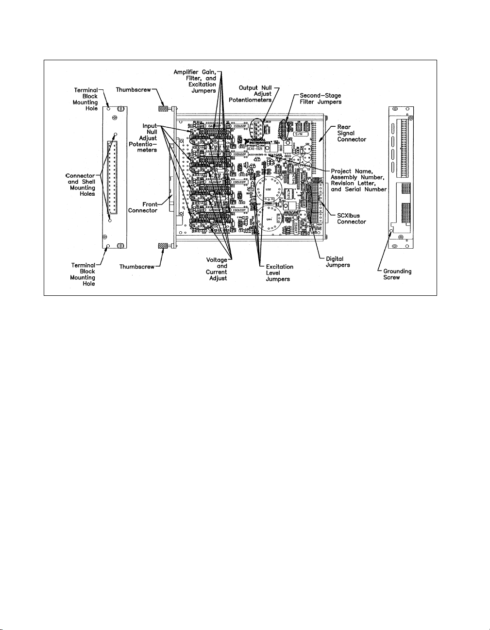
Figure 2-1. SCXI-1121 General Parts Locator Diagram.........................................2-2
Figure 2-2. SCXI-1121 Detailed Parts Locator Diagram........................................2-3
Figure 2-3. SCXI-1121 Front Connector Pin Assignment ......................................2-18
Figure 2-4. Ground-Referenced Signal Connection with
High Common-Mode Voltage ..............................................................2-21
Figure 2-5. Floating Signal Connection Referenced to Chassis Ground for
Better Signal-to-Noise Ratio.................................................................2-21
Figure 2-6. Floating AC-Coupled Signal Connection.............................................2-22
Figure 2-7. AC-Coupled Signal Connection with High Common-Mode Voltage.. 2-22
Figure 2-8. Assembling and Mounting the SCXI-1330
Connector-and-Shell Assembly ............................................................2-25
Figure 2-9. Nulling Circuit ......................................................................................2-29
Figure 2-10. Shunt Circuit.........................................................................................2-30
Figure 2-11. SCXI-1320 Parts Locator Diagram.......................................................2-36
Figure 2-12. SCXI-1328 Parts Locator Diagram.......................................................2-37
Figure 2-13. SCXI-1321 Parts Locator Diagram.......................................................2-38
Figure 2-14. SCXI-1121 Rear Signal Connector Pin Assignment ............................ 2-39
Figure 2-15. SCANCLK Timing Requirements........................................................2-43
Figure 2-16. Slot-Select Timing Diagram.................................................................2-44
Figure 2-17. Serial Data Timing Diagram.................................................................2-45
Figure 2-18. Configuration Register Write Timing Diagram....................................2-46
Figure 2-19. SCXI-1121 Module ID Register Timing Diagram ...............................2-47
Figure 3-1. SCXI-1121 Block Diagram...................................................................3-1
Figure 3-2. SCXIbus Connector Pin Assignment....................................................3-3
Figure 3-3. Digital Interface Circuitry Block Diagram ........................................... 3-6
Figure 3-4. SCXI-1121 Digital Control...................................................................3-7
Figure 3-5. Analog Input Block Diagram................................................................3-9
Figure 3-6. Analog Output Circuitry.......................................................................3-15
Figure 3-7. Single-Module Parallel Scanning .........................................................3-17
Figure 3-8. Single-Module Multiplexed Scanning (Direct) ....................................3-18
Figure 3-9. Single-Module Multiplexed Scanning (Indirect)..................................3-19
Figure 3-10. Multiple-Module Multiplexed Scanning...............................................3-19
Figure 3-11. Multiple-Chassis Scanning ...................................................................3-20
Figure B-1. SCXI-1121 Rear Signal Connector Pin Assignment ............................ B-1
Figure C-1. SCXIbus Connector Pin Assignment....................................................C-2
Figure D-1. SCXI-1121 Front Connector Pin Assignment......................................D-2
Figure E-1. SCXI-1340 Installation .........................................................................E-4
SCXI-1121 User Manual viii www.natinst.com
Page 8

Tables
Contents
Figure E-2. SCXI-1180 Rear Connections...............................................................E-9
Figure E-3. SCXI-1180 Front Panel Installation......................................................E-10
Figure E-4. Cover Removal......................................................................................E-11
Figure F-1. Revision A and B SCXI-1121 Signal Conditioning Module................F-1
Figure F-2. Revision A and B SCXI-1121 General Parts Locator Diagram............F-2
Figure F-3. Revision A and B SCXI-1121 Detailed Parts Locator Diagram...........F-3
Table 2-1. Digital Signal Connections, Jumper Settings........................................2-6
Table 2-2. Jumper W33 Settings.............................................................................2-8
Table 2-3. Gain Jumper Allocation.........................................................................2-9
Table 2-4. Gain Jumper Positions...........................................................................2-9
Table 2-5. Filter Jumper Allocation........................................................................2-10
Table 2-6. Voltage and Current Mode Excitation Jumper Setup............................2-11
Table 2-7. Maximum Load per Excitation Channel...............................................2-12
Table 2-8. Excitation Level Jumper Selection........................................................2-12
Table 2-9. Completion Network Jumpers............................................................... 2-14
Table 2-10. Trimmer Potentiometer and Corresponding Channel ...........................2-27
Table 2-11. Nulling Resistors and Corresponding Channel.....................................2-27
Table 2-12. Jumper Settings of the Nulling Circuits................................................2-29
Table 2-13. Jumper Settings on the SCXI-1320 Terminal Block.............................2-33
Table 2-14. Jumper Settings on the SCXI-1328 Terminal Block.............................2-34
Table 2-15. Jumper Settings on the SCXI-1321 Terminal Block.............................2-34
Table 2-16. SCXIbus to SCXI-1121 Rear Signal Connector to
Data Acquisition Board Pin Equivalences ............................................2-42
Table 3-1. SCXIbus Equivalents for the Rear Signal Connector ...........................3-5
Table 3-2. Calibration Potentiometer Reference Designators................................3-14
Table 5-1. SCXI-1121 Rear Signal Connector Pin Equivalences ..........................5-2
Table E-1. SCXI-1121 and MIO-16 Pinout Equivalences......................................E-2
Table E-2. SCXI-1341 and SCXI-1344 Pin Translations.......................................E-5
Table E-3. SCXI-1342 Pin Translations .................................................................E-7
Table E-4. SCXI-1343 Pin Connections.................................................................E-14
© National Instruments Corporation ix SCXI-1121 User Manual
Page 9
About This Manual
This manual describes the electrical and mechanical aspects of the
SCXI-1121 and contains information concerning its operation and
programming. The SCXI-1121 is a member of the National Instruments
Signal Conditioning eXtensions for Instrumentation (SCXI) Series for the
National Instruments data acquisition plug-in boards. This board is
designed for signal conditioning of strain gauges, RTDs, thermistors,
thermocouples, volt and millivolt sources, and 4 to 20 mA sources or 0 to
20 mA process-current sources where high common-mode voltages exist.
The SCXI-1121 operates as four isolated input channels and four isolated
excitation channels. Each channel is isolated and independently
configurable via jumpers.
This manual describes the installation, basic programming considerations,
and theory of operation for the SCXI-1121.
Conventions
The following conventions appear in this manual:
<> Angle brackets that contain numbers separated by an ellipsis represent a
range of values associated with a bit or signal name—for example,
DBIO<3..0>.
This icon denotes a note, which alerts you to important information.
This icon denotes a caution, which advises you of precautions to take to
avoid injury, data loss, or a system crash.
This icon denotes a warning, which advises you of precautions to take to
avoid being electrically shocked.
bold Bold text denotes items that you must select or click on in the software,
such as menu items and dialog box options. Bold text also denotes
parameter names.
italic Italic text denotes variables, emphasis, a cross reference, or an introduction
to a key concept. This font also denotes text that is a placeholder for a word
or value that you must supply.
© National Instruments Corporation xi SCXI-1121 User Manual
Page 10

About This Manual
monospace Text in this font denotes text or characters that you should enter from the
keyboard, sections of code, programming examples, and syntax examples.
This font is also used for the proper names of disk drives, paths, directories,
programs, subprograms, subroutines, device names, functions, operations,
variables, filenames and extensions, and code excerpts.
monospace italic
Italic text in this font denotes text that is a placeholder for a word or value
that you must supply.
Related Documentation
The following documents contain information that you may find helpful as
you read this manual:
• AT-MIO-16 User Manual (part number 320476-01)
• AT-MIO-16D User Manual (part number 320489-01)
• AT-MIO-16F-5 User Manual (part number 320266-01)
• AT-MIO-16X User Manual (part number 320488-01)
• AT-MIO-64F-5 User Manual (part number 320487-01)
• Lab-LC User Manual (part number 320380-01)
• Lab-NB User Manual (part number 320174-01)
• Lab-PC User Manual (part number 320205-01)
• Lab-PC+ User Manual (part number 320502-01)
• MC-MIO-16 User Manual, Revisions A to C (part number 320130-01)
• MC-MIO-16 User Manual, Revision D (part number 320560-01)
• NB-MIO-16 User Manual (part number 320295-01)
• NB-MIO-16X User Manual (part number 320157-01)
• PC-LPM-16 User Manual (part number 320287-01)
• SCXI-1000/1001 User Manual (part number 320423-01)
SCXI-1121 User Manual xii www.natinst.com
Page 11

Introduction
This chapter describes the SCXI-1121; lists the contents of your
SCXI-1121 kit; describes the optional software, optional equipment, and
custom cables; and explains how to unpack the SCXI-1121 kit.
The SCXI-1121 consists of four isolated input channels and four isolated
excitation channels. The SCXI-1121 is a module for signal conditioning of
strain gauges, RTDs, thermistors, thermocouples, volt and millivolt
sources, 4 to 20 mA current sources, and 0 to 20 mA process-current
sources. The SCXI-1121 can operate in two output modes—the
Parallel-Output mode with all four input channels connected in parallel to
four data acquisition board channels, or the Multiplexed-Output mode with
all four channels multiplexed into a single data acquisition board channel.
The SCXI-1121 operates with full functionality with National Instruments
MIO-16 boards. The SCXI-1121 operates with full functionality with the
Lab-PC+ board in single-chassis SCXI systems. However, the Lab-PC+
cannot control multiple-chassis SCXI systems. You can use the Lab-NB,
the Lab-PC, the Lab-LC, and the PC-LPM-16 boards with the SCXI-1121,
but these boards can control only single-chassis SCXI systems and cannot
scan the module when it is configured in the Multiplexed-Output mode.
These boards can perform only single-channel reads in this mode. You can
also use the SCXI-1121 with other systems that comply with the
specifications give n in Chapter 2, Configuration and Installation. You can
multiplex several SCXI-1121s into a single channel, thus greatly increasing
the number of analog input signals that can be digitized.
1
The addition of a shielded terminal block provides screw terminals for easy
signal attachment to the SCXI-1121. In addition, a temperature sensor for
cold-junction compensation of thermocouples is included on the terminal
block. This cold-junction reference (CJR) is either multiplexed along with
the four input channels or connected by jumpers to a different channel of
the data acquisition board.
With the SCXI-1121, the SCXI chassis can serv e as a fast-scanning signal
conditioner for laboratory testing, production testing, and industrial
process monitoring.
© National Instruments Corporation 1-1 SCXI-1121 User Manual
Page 12

Chapter 1 Introduction
What Your Kit Should Contain
The contents of the SCXI-1121 kit (part number 776572-21) are listed as
follows:
Kit Component Part Number
SCXI-1121 module 181700-01
SCXI-1121 User Manual 320426-01
If your kit is missing any of the components, contact Nati onal Instruments .
Optional Software
This manual contains complete instructions for directly programming the
SCXI-1121. You can order separate software packages for controlling the
SCXI-1121 from National Instruments.
When you combine the PC, AT, and MC data acquisition boards with the
SCXI-1121, you can use LabVIEW for Windows or LabW indows for DOS.
LabVIEW and LabWindows are inno vativ e program development software
packages for data acquisition and control applications. LabVIEW uses
graphical programming, whereas LabWindows enhances Microsoft C and
QuickBASIC. Both packages include extensive libraries for data
acquisition, instrument control, data analysis, and graphical data
presentation.
Your National Instruments data acquisition board is shipped with the
NI-DA Q software. NI-DA Q has a library of functions that you can call from
your application programming environment. These functions include
routines for analog input (A/D conversion), buffered data acquisition
(high-speed A/D conversion), analog output (D/A conversion), waveform
generation, digital I/O, counter/timer, SCXI, RTSI, and self-calibration.
NI-DAQ maintains a consistent software interface among its different
versions so you can switch between platforms with minimal modifications
to your code.
You can also use the SCXI-1121, together with the PC, AT, and MC data
acquisition boards, with NI-DAQ software for DOS/Windows/
LabWindows/CVI. NI-DAQ software for DOS/Windows/
LabWindows/CVI comes with language interfaces for Professional
BASIC, T urbo Pascal, T urbo C, T urbo C++, Borland C++, and Microsoft C
SCXI-1121 User Manual 1-2 www.natinst.com
Page 13

Chapter 1 Introduction
for DOS and Visual Basic, Turbo Pascal, Microsoft C with SDK,
and Borland C++ for Windows. NI-DAQ software for
DOS/Windows/LabWindows is on high-density 5.25 in. and 3.5 in.
diskettes.
You can use the SCXI-1121, together with the Lab-LC or NB Series data
acquisition boards, with LabVIEW for Macintosh, a software system that
features interactive graphics, a state-of-the-art user interface, and a
powerful graphical programming language. The LabVIEW Data
Acquisition VI Library, a series of VIs for using LabVIEW with National
Instruments boards, is included with LabVIEW. The LabVIEW Data
Acquisition VI Library is functionally equivalent to the NI-DAQ software
for Macintosh.
You can also use the SCXI-1121, combined with the NB Series data
acquisition boards, with NI-DAQ software for Macintosh. NI-DAQ
software for Macintosh, which is shipped with all National Instruments
Macintosh data acquisition boards, comes with language interfaces for
MPW C, THINK C, Pascal, and Microsoft QuickBASIC. Any language
that uses Device Manager Toolbox calls can access NI-DAQ software for
Macintosh.
© National Instruments Corporation 1-3 SCXI-1121 User Manual
Page 14
Chapter 1 Introduction
Optional Equipment
NB6 cable
0.5 m 181305-01
1.0 m 181305-10
SCXI-1320 front terminal block 776573-20
SCXI-1321 offset-null and shunt-calibration terminal block 776573-21
SCXI-1328 high-accuracy isothermal terminal block 776573-28
SCXI-1330 32-pin connector-and-shell assembly 776573-30
SCXI-1340 cable assembly 776574-40
SCXI-1341 Lab-NB/Lab-PC/Lab-PC+ cable assembly 776574-41
SCXI-1342 PC-LPM-16 cable assembly 776574-42
SCXI-1343 rear screw terminal adapter 776574-43
SCXI-1344 Lab-LC cable assembly 776574-44
SCXI-1346 shielded multichassis cable adapter 776574-46
Equipment Part Number
SCXI-1347 SCXI shielded cable assembly
with 1 m cable 776574-471
with 2 m cable 776574-472
with 5 m cable 776574-475
with 10 m cable 776574-470
SCXI-1349 SCXI shielded cable assembly
with 1 m cable 776574-491
with 2 m cable 776574-492
with 5 m cable 776574-495
with 10 m cable 776574-490
SCXI-1350 multichassis adapter 776575-50
SCXI process-current resistor kit 776582-01
Standard ribbon cable
0.5 m 180524-05
1.0 m 180524-10
SCXI-1121 User Manual 1-4 www.natinst.com
Page 15

Custom Cables
Chapter 1 Introduction
Refer to the Signal Connections section in Chapter 2, Configuration and
Installation, and to Appendix E, SCXI-1121 Cabling, for additional
information on cabling, connectors, and adapters.
The SCXI-1121 rear signal connector is a 50-pin male ribbon-cable header.
The manufacturer part number used by National Instruments for this header
is as follows:
• AMP Inc. (part number 1-103310-0)
The mating connector for the SCXI-1121 rear signal connector is a
50-position polarized ribbon-socket connector with strain relief. National
Instruments uses a polarized or keyed connector to prevent inadvertent
upside-down connection to the SCXI-1121. Recommended manufacturer
part numbers for this mating connector are as follows:
• Electronic Products Division/3M (part number 3425-7650)
• T&B/Ansley Corporation (part number 609-5041CE)
Standard 50-conductor, 28 AWG, stranded ribbon cables that can be used
with these connectors are as follows:
• Electronic Products Division/3M (part number 3365/50)
• T&B/Ansle y Corporation (part number 171-50)
The SCXI-1121 front connector is a 32-pin DIN C male connector with
column A and column C even pins only. The manufacturer part number
used by National Instruments for this connector is as follows:
• Panduit Corporation (part number 100-932-023)
The mating connector for the SCXI-1121 front connector is a 32-pin DIN C
female connector. National Instruments uses a polarized connector to
prevent inadvertent upside-down connection to the SCXI-1121.
Recommended manufacturer part numbers for this mating connector are as
follows:
• Panduit Corporation (part number 100-932-434 straight-solder
eyelet pins)
• Panduit Corporation (part number 100-932-633; right-angle pins)
National Instruments selected these connectors to meet UL 1950 and
UL 1244 for 1,500 V
© National Instruments Corporation 1-5 SCXI-1121 User Manual
isolation.
rms
Page 16

Chapter 1 Introduction
Unpacking
Your SCXI-1121 module is shipped in an antistatic package to prevent
electrostatic damage to the module. Several components on the module can
be damaged by electrostatic discharge. To avoid such damage in handling
the module, take the following precautions.
• Touch the antistatic package to a metal part of your SCXI chassis
before removing the module from the package.
• Remo ve the module from the package and inspect the module for loose
components or any other sign of damage. Notify National Instruments
if the module appears damaged in any way. Do not install a damaged
module into your SCXI chassis.
SCXI-1121 User Manual 1-6 www.natinst.com
Page 17
Configuration and Installation
This chapter describes the SCXI-1121 jumper configurations, installation
of the SCXI-1121 into the SCXI chassis, signal connections to the
SCXI-1121, and cable wiring.
Module Configuration
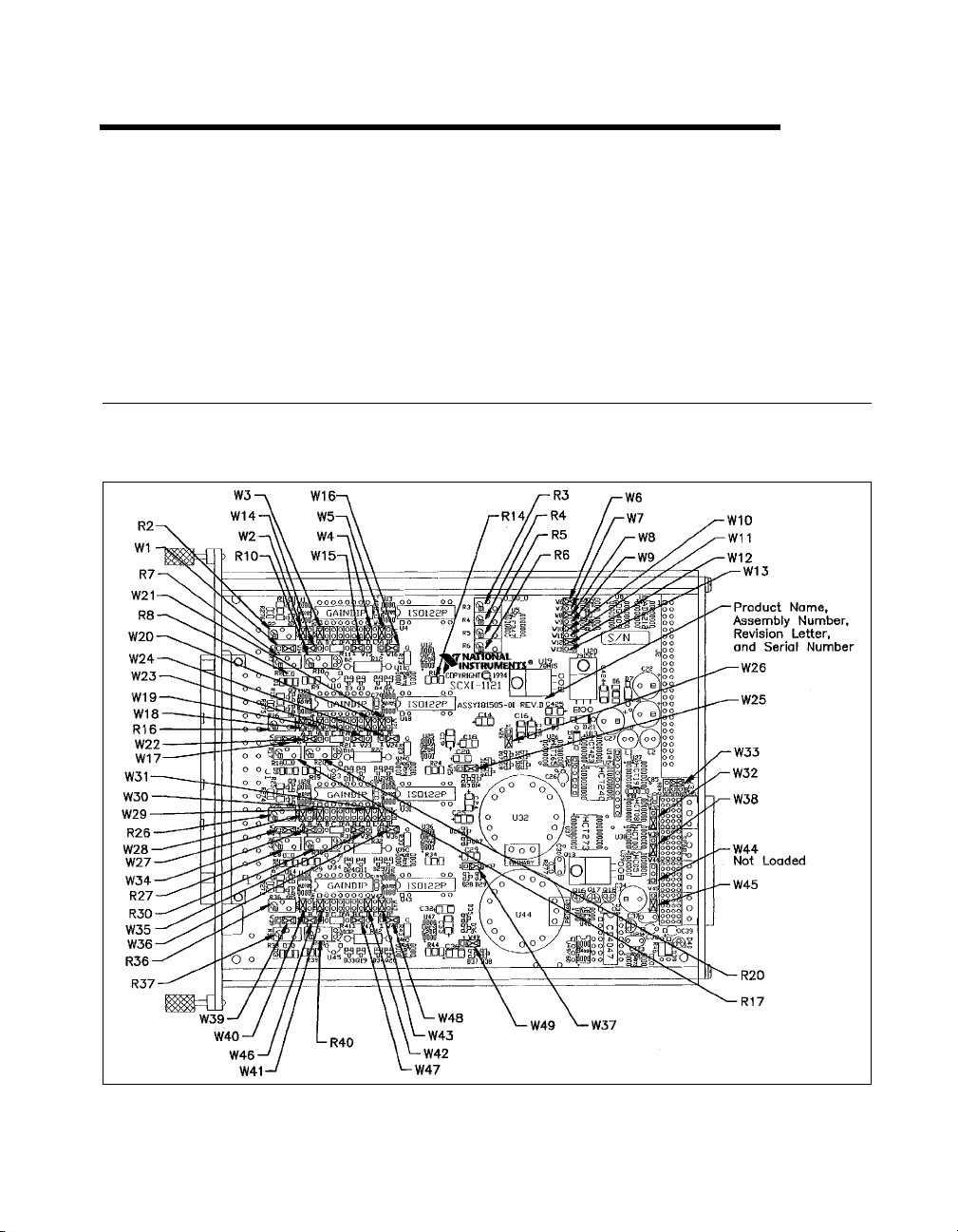
The SCXI-1121 contains 49 jumpers that are shown in the parts locator
diagrams in Figures 2-1 and 2-2.
2
Figure 2-1.
© National Instruments Corporation 2-1 SCXI-1121 User Manual
SCXI-1121 General Parts Locator Diagram
Page 18
Chapter 2 Configuration and Installation
Figure 2-2. SCXI-1121 Detailed Parts Locator Diagram
The jumpers are used as follows:
• Fixed jumpers
– On Revision A and B modules, jumper W32 is unused and should
not be connected.
– Jumper W45 is reserved and should not be reconfigured.
– On Revision A and B modules, jumper W44 carries the
SLOT0SEL* signal from the rear signal connector, after
buffering, to the SCXIbus INTR* line and should be left in the
factory-set position (position 1). On Revision C or later modules,
jumper W44 does not exist.
• User-configurable jumpers
– Jumper W38 carries the SCXIbus MISO line, after buffering, to
the SERDATOUT signal on the rear signal connector.
– On Revision C or later modules, jumper W32 connects a pullup
resistor to the SERDATOUT signal on the rear signal connector.
– Jumper W33 configures the guard, the analog output ground, and
enables the Pseudodifferential Reference mode.
SCXI-1121 User Manual 2-2 www.natinst.com
Page 19

Chapter 2 Configuration and Installation
– Jumpers W3, W19, W29, and W41 configure the first-stage gain
of input channels 0 through 3, respectively.
– Jumpers W4, W20, W30, and W42 configure the second-stage
gain of input channels 0 through 3, resp ectively.
– Jumpers W5, W21, W31, and W43 configure the first-stage
filtering of input channels 0 through 3, respectively.
– Jumpers W6 and W7, W8 and W9, W10 and W11, and W12 and
W13 configure the second-stage filtering of input channels 0
through 3, respectively.
– Jumpers W14 and W15, W22 and W23, W34 and W35, and W46
and W47 configure the voltage or current mode of operation for
excitation channels 0 through 3, respectively.
– Jumpers W16 and W26, W24 and W25, W36 and W37, and W48
and W49 configure the level of excitation for excitation channels
0 through 3, respectively.
– Jumpers W1 and W2, W17 and W18, W27 and W28, and W39
and W40 configure the half-bridge completion network for
channels 0 through 3, respectively.
Further configuration of the board is software controlled and will be
discussed later in this chapter.
Digital Signal Connections
The SCXI-1121 has three jumpers dedicated for communication between
the data acquisition board and the SCXIbus. These jumpers are W32, W38,
and W44.
Jumper W44
Position 1 on Revision A and B modules connects, after buffering,
SLOT0SEL* to the SCXIbus INTR* line. This is the factory-default setting
and should not be changed. In this setting, the data acquisition board
controls the SCXIbus INTR* line. See the Timing Requirements and
Communication Protocol section later in this chapter, and Chapter 5,
Programming, for information on the use of the INTR* line. See
Appendix E, SCXI-1121 Cabling, for the pin equivalences of the
SCXI-1121 rear signal connector and the data acquisition board
I/O connector.
Position 3 is reserved and should not be used. This position is not explicitly
marked on the module.
© National Instruments Corporation 2-3 SCXI-1121 User Manual
Page 20

Chapter 2 Configuration and Installation
On Revision C or later modules, jumper W44 does not exist. SLOT0SEL*
is always buffered to the INTR* line.
Jumper W38
Position 1 connects, after buffering, the SCXIbus MISO line to the
SERDATOUT pin of the rear signal connector. In this setting, along with
the proper setting of W32, the data acquisition board can read the Module
ID Register of the SCXI-1121. See the Timing Requirements and
Communication Protocol section later in this chapter, and Chapter 4,
Register Descriptions, for information on reading the Module ID Register.
See Appendix E, SCXI-1121 Cabling, for the pin equivalences of the
SCXI-1121 rear signal connector and the data acquisition board I/O
connector. This is the factory-default setting.
Position 3 disconnects SERDATOUT from the SCXIbus MISO line.
Jumper W32
On Revision A and B modules, jumper W32 should not be connected. On
Revision C or later modules, Position 1 connects a 2.2 kΩ pullup resistor
to the SERDATOUT line (factory-default setting), and Position 3 does not
connect the pullup resistor to the SERDATOUT line.
Using Jumpers W32 and W38
Set jumpers W32 and W38 as follows:
If the SCXI-1121 is not cabled to a data acquisition board, the positions of
these jumpers do not matter, so leav e them in their factory default positions
(both in position 1).
If the SCXI-1121 is cabled to a data acquisition board, and the SCXI
chassis that the SCXI-1121 is in, is the only SCXI chassis cabled to that
data acquisition board, leave the jumpers in their factory default positions
(both in position 1).
If the SCXI-1121 is cabled to a data acquisition board, and there are
multiple SCXI chassis cabled to that data acquisition board with shielded
cables (you are using SCXI-1346 shielded cable multi-chassis adapters),
leave the jumpers in their factory default positions (both in position 1).
If the SCXI-1121 is cabled to a data acquisition board, and there are
multiple SCXI chassis cabled to that data acquisition board with ribbon
cables (you are using SCXI-1350 multi-chassis adapters), leave jumper
SCXI-1121 User Manual 2-4 www.natinst.com
Page 21

Chapter 2 Configuration and Installation
W38 in its factory default position (position 1). On all but one of the
SCXI-1121s that are cabled to the data acquisition board, move jumper
W32 to position 3. It does not matter which of the SCXI-1121 modules that
are cabled to the data acquisition board has jumper W32 set to position 1.
If you have different types of modules cabled to the data acquisition board,
those different modules will have jumpers similar to W38 and W32 of the
SCXI-1121. Set those jumpers on the different modules using the same
method described here for the SCXI-1121.
On Revision A and B SCXI-1121s, jumper W32 is not used. Y ou set jumper
W38 as explained in the cases above, except in the case of a multiple
chassis ribbon cable system. In a multichassis ribbon cable system with
Revision A and B SCXI-1121s cabled to the data acquisition board, you can
access the MISO line in only one chassis. Pick one of the chassis and set
jumper W38 to position 1 on the SCXI-1121 in that chassis that is cabled
to the data acquisition board. On the SCXI-1121s that are in the other
chassis and cabled to the data acquisition board, set jumper W38 to
position 3. Notice that you will only be able to access digital information
from the chassis that has the SCXI-1121 with jumper W38 set to position 1.
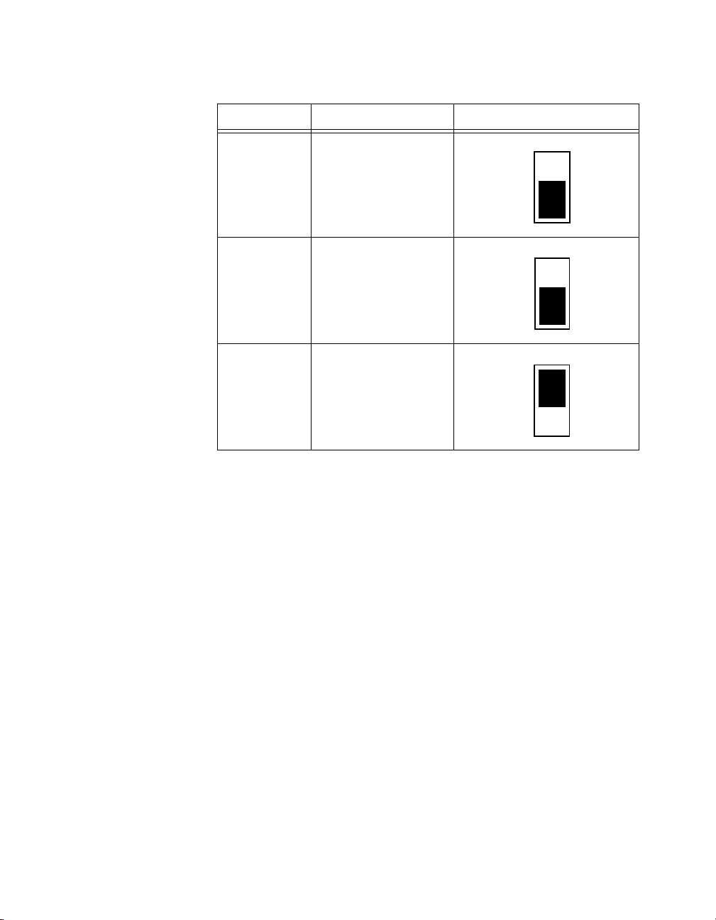
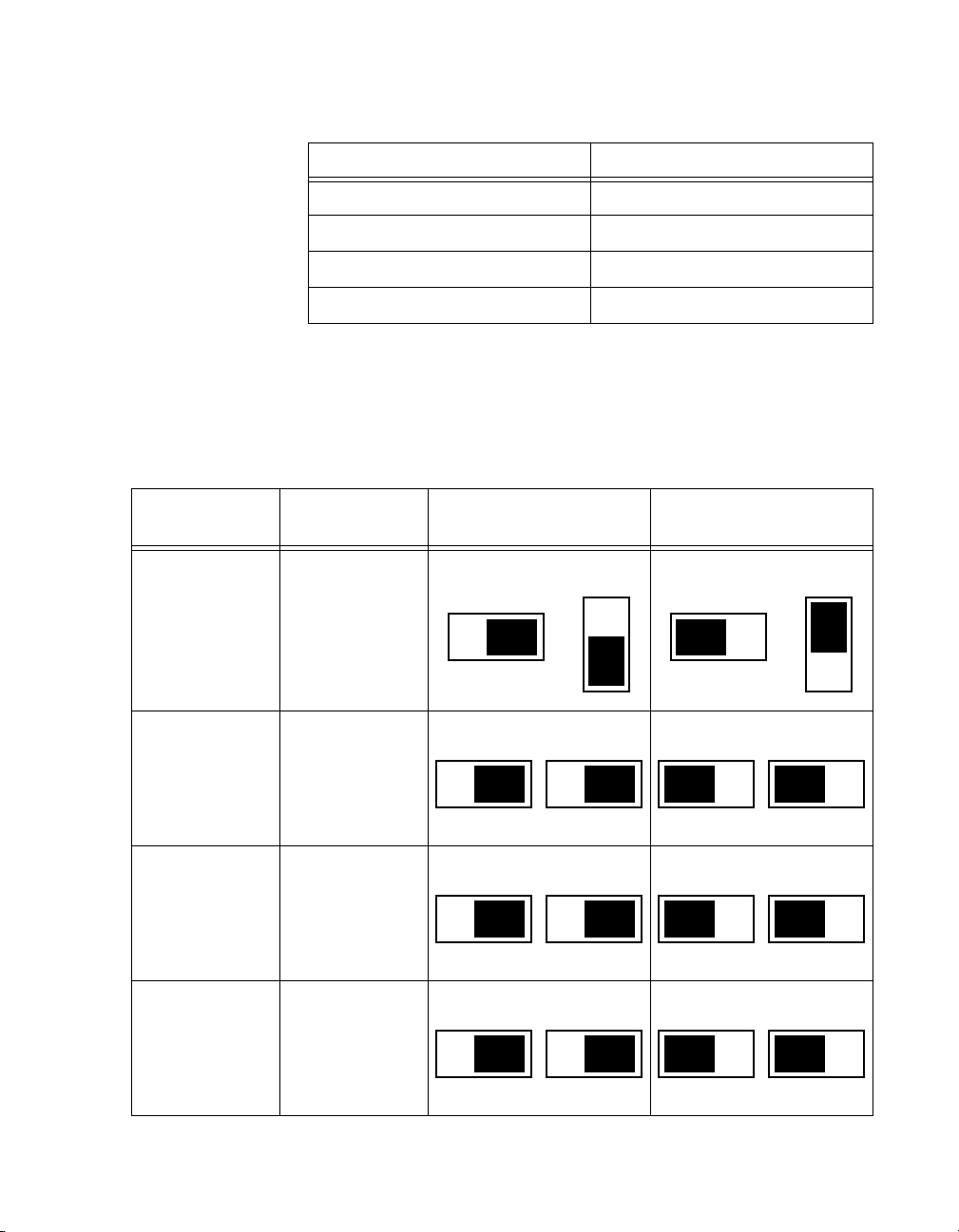
Table 2-1. Digital Signal Connections, Jumper Settings
Jumper Description Configuration
W38 Factory setting;
connects MISO to
SERDATOUT
3
•
2
•
1
•
W38 Parking position
3
•
2
•
1
•
W45 Factory setting
3
•
2
•
1
•
© National Instruments Corporation 2-5 SCXI-1121 User Manual
Page 22
Chapter 2 Configuration and Installation
Analog Configuration
The SCXI-1121 has 45 analog configuration jumpers.
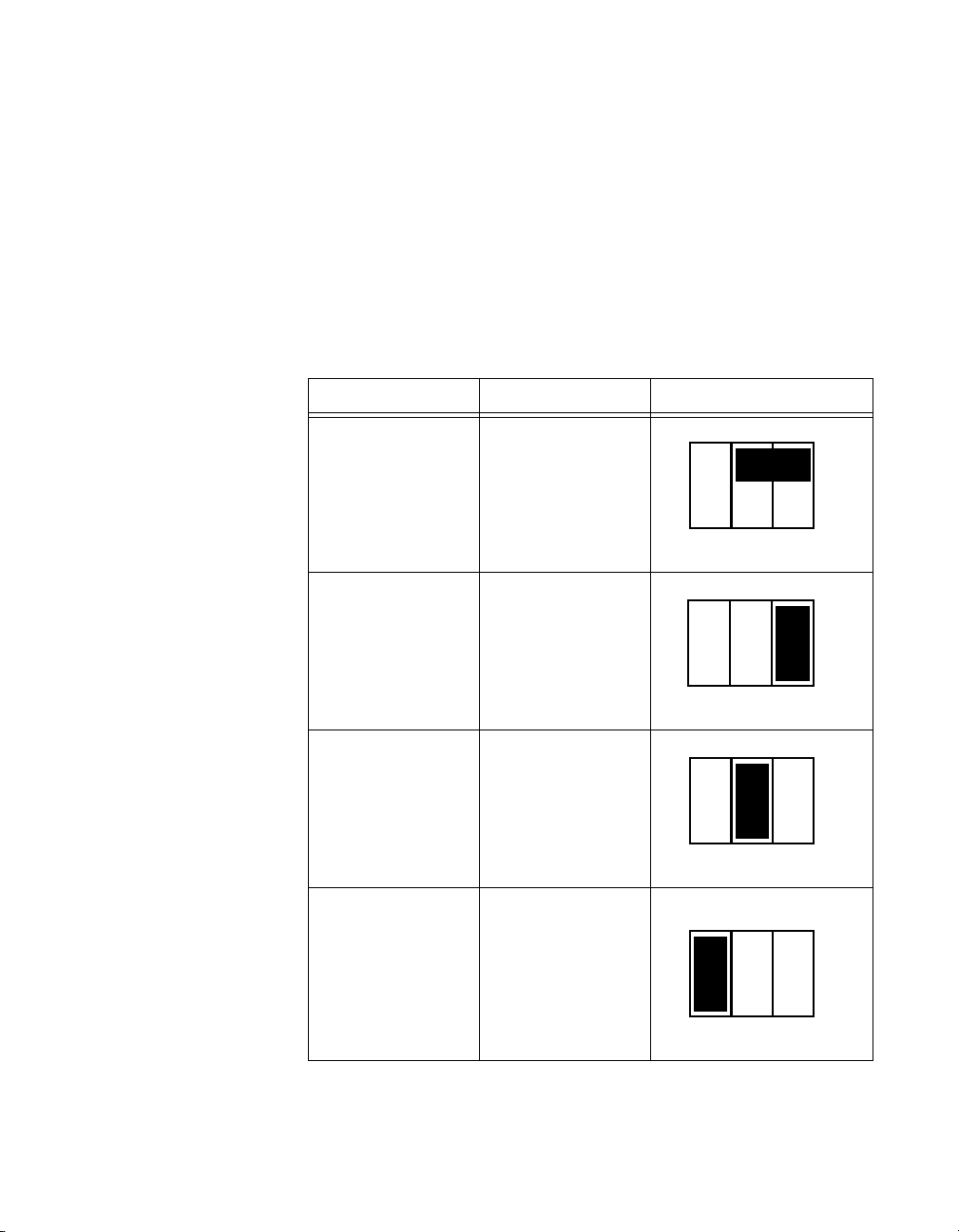
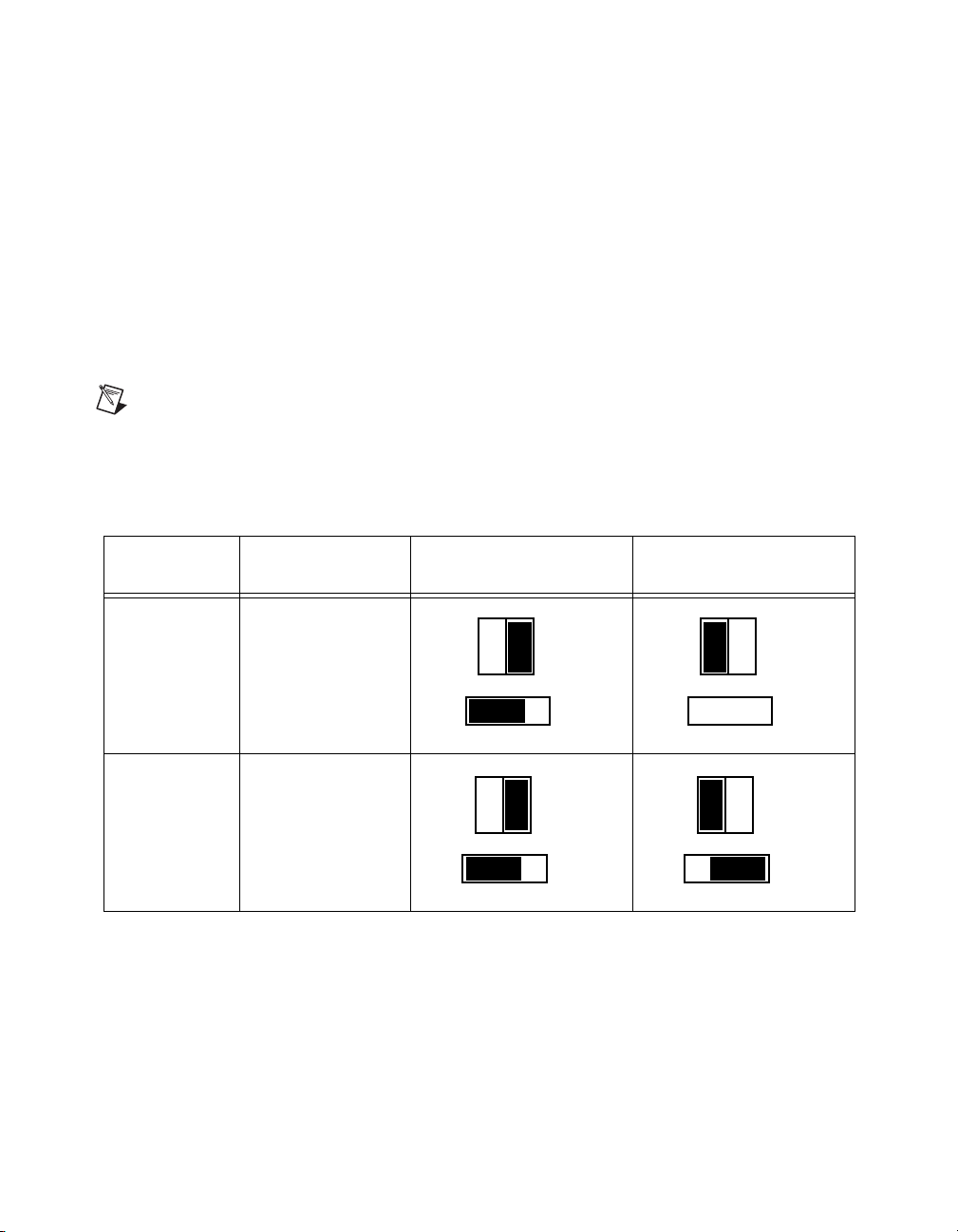
Table 2-1.
Jumper Description Configuration
W44 Factory setting
W32 Fatory-default setting;
W32 Parking position (not
Digital Signal Connections, Jumper Settings (Continued)
(Revision A and B
modules only)
connects pullup to
SERDATOUT
(Revision C and later)
connected on
Revision A or B
modules)
3
•
2
•
1
•
3
•
2
•
1
•
3
•
2
•
1
•
Before starting, notice that the jumper configurations for each input
channel and each excitation channel are similar only the jumper numbers
differ . Therefore, when you learn ho w to set up one channel pair (input and
excitation), you can set up the other channel pairs as well.
Grounding, Shielding, and Reference Mode Selection
Jumper W33
Position AB-R0 connects the analog reference to the analog output ground
(pins 1 and 2 on the rear signal connector). Select this configuration if you
are using an RSE data acquisition board. It is not recommended to use a
differential input data acquisition board when jumper W33 is in the AB-R0
position.
SCXI-1121 User Manual 2-6 www.natinst.com
Page 23
Chapter 2 Configuration and Installation
•••••
•
A
B
R2 R 1 R 0
•••••
•
A
B
R2 R 1 R 0
•••••
•
A
B
R2 R 1 R 0
•••••
•
A
B
R2 R 1 R 0
Position AB-R1 connects the analog reference to the SCXIbus guard.
Position A-R0R1 is the parking position and the factory setting.
Position AB-R2 enables the Pseudodifferential Reference mode and
connects the analog reference to the OUTREF pin on the rear signal
connector. Select this mode when the SCXI-1121 has to operate with data
acquisition boards that have a nonreferenced single-ended (NRSE) input. It
is not recommended to use differential-input data acquisition boards when
jumper W33 is in the AB-R2 position.
Table 2-2. Jumper W33 Settings
Jumper Description Configuration
W33 Factory setting in
parking position
W33 Connects the
analog reference to
AOGND (pins 1
and 2 of the rear
signal connector)
W33 Connects SCXIbus
guard to the analog
reference
W33 Enables the
Pseudodifferential
Reference mode
(pin 19 of the rear
signal connector is
connected to the
analog reference)
© National Instruments Corporation 2-7 SCXI-1121 User Manual
Page 24
Chapter 2 Configuration and Installation
Input Channel Jumpers
Gain Jumpers
Each input channel has two gain stages. The first gain stage provides gains
of 1, 10, 50, and 100 and the second stage provides gains of 1, 2, 5, 10, and
20. Tables 2-3 and 2-4 show how to set up the gain for each channel.
Table 2-3.
Input Channel
Number
Gain Jumper Allocation
First Gain
Jumper
Second Gain
Jumper
0 W3 W4
1 W19 W20
2 W29 W30
3 W41 W42
The board is shipped to you with the first-stage gain set to 100 (position A)
and a second-stage gain set to 10 (position D). To change the gain of your
module, move the appropriate jumper on your module to the position
indicated in T able 2-4. Refer to Figure 2-2 for the jumper locations on your
module.
T o determine the o verall g ain of a giv en channel use the follo wing formula:
Overall gain = First-stage gain × second-stage gain
Table 2-4.
Gain Jumper Positions
Gain Setting Jumper Position
First-stage 1
10
50
100
A (factory setting)
Second-stage 1
2
5
10
D (factory setting)
20
SCXI-1121 User Manual 2-8 www.natinst.com
D
C
B
A
B
C
E
Page 25

Chapter 2 Configuration and Installation
Filter Jumpers
Two-stage filtering is also available on your SCXI-1121 module. The first
stage is located in the isolated section of the input channel, whereas the
second stage is located in the nonisolated section of the input channel. This
permits a higher signal-to-noise ratio by eliminating the noise generated by
the isolation amplifier. Furthermore, two filter bandwidths are
available—10 kHz and 4 Hz.
Table 2-5.
First Filter Jumper Second Filter Jumper
Input Channel
Number
0 W5-A W5-B W6 W7
1 W21-A W21-B W8 W9
2 W31-A W31-B W10 W11
3 W43-A W43-B W12 W13
4 Hz
(Factory Setting)
Your SCXI-1121 is shipped in the 4 Hz configuration. Always make sure
to set both stages to the same bandwidth. This will ensure that the required
bandwidth is achieved.
Filter Jumper Allocation
10 kHz
4 Hz
(Factory Setting)
Excitation Jumpers
Current and Voltage Excitation Jumpers
You can configure each excitation channel of your SCXI-1121 to either a
Voltage or Current excitation mode. Each channel has two jumpers for this
purpose. Set both jumpers in the same mode for correct operation of the
excitation channel. Refer to Table 2-6 for setting up your module in the
mode you want. Your SCXI-1121 is shipped to you in the Voltage mode.
10kHz
© National Instruments Corporation 2-9 SCXI-1121 User Manual
Page 26
Chapter 2 Configuration and Installation
•
•
•
W14
1 2 3
•
•
•
W15
1 2 3
•
•
•
W22
1 2 3
•
•
•
W23
1 2 3
•
•
•
W34
1 2 3
•
•
•
W35
1 2 3
•
•
•
W46
1 2 3
•
•
•
W47
1 2 3
Table 2-6.
Excitation
Channel
Jumpers
0 W14 and W15
1 W22 and W23
2 W34 and W35
3 W46 and W47
Voltage and Current Mode Excitation Jumper Setup
Voltage Mode
(Factory Setting)
W14
•
•
•
1 2 3
W22
•
•
1 2 3
W34
•
•
1 2 3
W46
•
•
•
•
•
•
1 2 3
•
1 2 3
•
1 2 3
•
W15
•
W23
•
W35
•
W47
•
•
•
•
•
Current Mode
1 2 3
1 2 3
Excitation Level
Each excitation channel of your SCXI-1121 has two different current or
voltage levels. You can set a given channel to one of the following level
modes:
• In the Current mode 0.150 or 0.450 mA
• In the Voltage mode 3.333 or 10 V
It is important to notice that you should select the level of excitation
according to the load you are using. Table 2-7 lists the maximum load that
can be driven per channel at each level of excitation for both volt and
current excitation.
SCXI-1121 User Manual 2-10 www.natinst.com
Page 27
Chapter 2 Configuration and Installation
•
•
•
W16
1 2 3
•
•
•
W26
1
2
3
•
•
•
W24
1 2 3
•
•
•
W25
1 2 3
•
•
•
W36
1 2 3
•
•
•
W37
1 2 3
•
•
•
W48
1 2 3
•
•
•
W49
1 2 3
Table 2-7. Maximum Load per Excitation Channel
Excitation Level Maximum Load
3.333 V 28 mA
10 V 14 mA
0.150 mA 10 kΩ
0.450 mA 10 kΩ
After selecting the excitation mode of operation desired—Voltage or
Current—as described in the previous section, use Table 2-8 to set your
SCXI-1121 for the level of operation. Your SCXI-1121 is shipped with the
Voltage mode set to 3.333 V.
Table 2-8. Excitation Level Jumper Selection
Excitation
Channel
0 W16 and W26
1 W24 and W25
2 W36 and W37
3 W48 and W49
Jumpers
3.333 V or 0.150 mA
(Factory Setting)
W16
•
•
1 2 3
W24
•
•
1 2 3
W36
•
•
1 2 3
W48
•
•
•
•
•
1
•
2
3
W25
•
1 2 3
W37
•
1 2 3
W49
•
W26
•
•
•
10 V or 0.450 mA
•
•
•
•
•
•
1 2 3
© National Instruments Corporation 2-11 SCXI-1121 User Manual
1 2 3
Page 28
Chapter 2 Configuration and Installation
A B
W18
W17
1 2 3
•••
•
•
•
•
Using the Internal Half-Bridge Completion
Your SCXI-1121 includes half-bridge completion for half-bridge and
quarter-bridge setups. The completion network consists of two
4.5 kΩ ± 0.05% ratio tolerance resistors with a temperature coefficient of
5 ppm/°C. These resistors are connected in series. To enable the network,
you must set two jumpers for each input/excitation channel pair.
When the completion network is enabled, you cannot access the negative
input of the amplifier, which preserves the overvoltage protection of the
channel. Table 2-9 shows how to enable and disable the completion
network.
Note
When using the half-bridge completion network with a quarter-bridge setup, you
must use an extra resistor to complete the bridge. Place this resistor on the terminal block
between the positive input channel and the negative excitation output.
Table 2-9.
Completion Network Jumpers
Channel Jumpers Enable Completion
0 W1 and W2
•••
W2
•
A B
•
•
•
W1
1 2 3
1 W17 and W18
•••
W18
•
A B
•
•
•
W17
1 2 3
Disable Network
(Factory Setting)
•••
W2
•
A B
•
•
•
W1
1 2 3
SCXI-1121 User Manual 2-12 www.natinst.com
Page 29

Table 2-9. Completion Network Jumpers (Continued)
A B
W28
W27
1 2 3
•••
•
•
•
•
A B
W40
W39
1 2 3
•••
•
•
•
•
Channel Jumpers Enable Completion
Chapter 2 Configuration and Installation
Disable Network
(Factory Setting)
2 W27 and W28
3 W39 and W40
•••
•
A B
•
•
1 2 3
•••
•
A B
•
•
1 2 3
W28
•
W40
•
W27
W39
© National Instruments Corporation 2-13 SCXI-1121 User Manual
Page 30

Chapter 2 Configuration and Installation
Hardware Installation
You can install the SCXI-1121 in any available SCXI chassis. After you
have made any necessary changes and have verified and recorded the
jumper settings on the form in AppendixG, Technical Support Resources,
you are ready to install the SCXI-1121. The following are general
installation instructions consult the user manual or technical reference
manual of your SCXI chassis for specific instructions and warnings.
1. Turn off the computer that contains the data acquisition board or
disconnect it from your SCXI chassis.
2. Turn off the SCXI chassis. Do not insert the SCXI-1121 into a chassis
that is turned on.
3. Insert the SCXI-1121 into the board guides. Gently guide the module
into the back of the slot until the connectors make good contact. If a
cable assembly has already been installed in the rear of the chassis, the
module and cable assembly must be firmly engaged; however, do not
force the module into place.
4. Screw the front mounting panel of the SCXI-1121 to the top and
bottom threaded strips of your SCXI chassis.
5. If this module is to be connected to an MIO-16 data acquisition board,
attach the connector at the metal end of the SCXI-1340 cable assembly
to the rear signal connector on the SCXI-1121 module. Screw the rear
panel to the rear threaded strip. Attach the loose end of the cable to the
MIO-16 board.
Note
For installation procedures with other SCXI accessories and data acquisition boards,
consult Appendix E, SCXI-1121 Cabling.
6. Check the installation.
7. Turn on the SCXI chassis.
8. Turn on the computer or reconnect it to your chassis.
The SCXI-1121 module is installed and ready for operation.
SCXI-1121 User Manual 2-14 www.natinst.com
Page 31

Signal Connections
This section describes the input and output signal connections to the
SCXI-1121 board via the SCXI-1121 front connector and rear signal
connector, and includes specifications and connection instructions for the
signals given on the SCXI-1121 connectors.
Chapter 2 Configuration and Installation
Cautions
flammable gasses or fumes.
Keep away from live circuits. Do not remove equipment covers or shields unless you are
trained to do so. If signal wires are connected to the device, hazardous voltages may exist
even when the equipment is turned off. To avoid a shock hazard, do not perform procedures
involving co ver or shield remo v al unless you are qualified to do so and disconnect all field
power prior to removing covers or shields.
Equipment described in this document must be used in an Installation Category II
environment per IEC 60664. This category requires local level supply mains-connected
installation.
Do not operate damaged equipment. The safety protection features built into this device
can become impaired if the device becomes damaged in any way . If the device is damaged,
turn the device off and do not use until service-trained personnel can check its safety. If
necessary , return the device to National Instruments for service and repair to ensure that its
safety is not compromised.
Do not operate this equipment in a manner that contradicts the information specif ied in this
document. Misuse of this equipment could result in a shock hazard.
Terminals are for use only with equipment that has no accessible live parts.
Do not substitute parts or modify equipment. Because of the danger of introducing
additional hazards, do not install unauthorized parts or modify the device. Return the
device to National Instruments for service and repair to ensure that its safety features are
not compromised.
Do not operate the device in an explosive atmosphere or where there may be
When using the device with high common-mode voltages, you must insulate your signal
wires for the highest input voltage. National Instruments is not liable for any damages or
injuries resulting from inadequate signal wire insulation. Use only 26-14 AWG wire with
a voltage rating of 300 V and 60 °C for measuring 250 V. Prepare your signal wire by
stripping the insulation no more than 7 mm.
© National Instruments Corporation 2-15 SCXI-1121 User Manual
Page 32

Chapter 2 Configuration and Installation
When connecting or disconnecting signal lines to the SCXI terminal block screw terminals,
make sure the lines are powered off. Potential differences between the lines and the SCXI
ground create a shock hazard while you connect the lines.
Connect the signal wires to the screw terminals by inserting the stripped end of the wire
fully into the terminals. Tighten the terminals to a torque of 5 to 7 in.-lb.
Connections, including power signals to ground and vice versa, that exceed any of the
maximum signal ratings on the SCXI device can create a shock or fi re hazard or can
damage any or all of the boards connected to the SCXI chassis, the host computer, and the
SCXI device. National Instruments is not liable for any damages or injuries resulting from
incorrect signal connections.
If high voltages (≥30 Vrms and 42.4 V peak or 60 VDC) are present, you must connect a
safety earth ground wire to the terminal block safety ground solder lug. This complies with
safety agency requirements and protects against electric shock when the terminal block is
not connected to the chassis. T o connect the safety earth ground to the safety ground solder
lug, run an earth ground wire in the cable from the signal source to the terminal block.
National Instruments is not liable for any damages or injuries resulting from inadequate
safety earth ground connections.
Do not loosen or re-orient the safety ground solder lug hardware when connecting the
safety ground wire. To do so reduces the safety isolation between the high voltage and
safety ground.
Clean devices and terminal blocks by brushing off light dust with a soft, nonmetallic brush.
Remove other contaminants with deionized water and a stiff nonmetallic brush. The unit
must be completely dry and free from contaminants before returning to service.
Use only National Instruments TBX Series cable assemblies with high-voltage TBX Series
terminal blocks.
Front Connector
Figure 2-3 shows the pin assignments for the SCXI-1121 front connector.
SCXI-1121 User Manual 2-16 www.natinst.com
Page 33
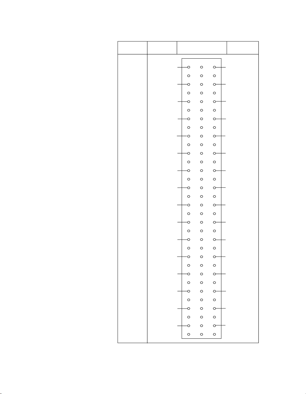
Chapter 2 Configuration and Installation
Pin
Number
32
31
30
29
28
27
26
25
24
23
22
21
20
19
18
17
16
15
14
13
12
11
10
9
8
7
6
5
4
3
2
1
Signal
Name
CH0+
EX0+
EGND0
CH1+
EX1+
EGND1
CH2+
EX2+
EGND2
CH3+
EX3+
EGND3
SCAL
+5 V
CGND
Column
A B C
Signal
Name
CH0–
EX0+
CH1–
EX1–
CH2–
EX2–
CH3–
EX3–
RSVD
RSVD
MTEMP
DTEMP
Figure 2-3. SCXI-1121 Front Connector Pin Assignment
© National Instruments Corporation 2-17 SCXI-1121 User Manual
Page 34

Chapter 2 Configuration and Installation
Front Connector Signal Descriptions
Pin Signal Name Description
A2 CGND Chassis Ground—This pin is tied to the SCXI chassis.
C2 DTEMP Direct Temperature Sensor—This pin connects the
temperature sensor to the MCH4+ when the terminal block
is configured for direct temperature connection.
A4 +5 V +5 VDC Source—This pin is used to power the
temperature sensor on the terminal block. 0.2 mA of source
not protected.
C4 MTEMP Multiplexed Temperature Sensor—This pin connects the
temperature sensor to the output multiplexer.
A6 SCAL Shunt Calibration—This pin is tied to the SCAL bit and is
used to control the SCXI-1321 shunt calibration switch.
CMOS/TTL output not protected.
C6, C8 RSVD Reserved—These pins are reserved. Do not connect any
signal to these pins.
A8, C10, C16,
C22, C28
A10 EGND3 Excitation Ground 3—This pin connects to the excitation
A12 EX3+ Positiv e Excitation Output 3—This pin is connected to the
C12 EX3– Negative Excitation Output 3—This pin is connected to the
A14 CH3+ Positive Input Channel 3—This pin is connected to the
C14 CH3– Negative Input Channel 3—This pin is connected to the
A16 EGND2 Excitation Ground 2—This pin connects to the excitation
A18 EX2+ Positiv e Excitation Output 2—This pin is connected to the
C18 EX2– Negative Excitation Output 2—This pin is connected to the
No Connect Do not connect any signal to these pins.
ground 3 via a 51 kΩ resistor.
excitation channel 3 positive output.
excitation channel 3 negative output.
input channel 3 positive input.
input channel 3 negative input.
ground 2 via a 51 kΩ resistor.
excitation channel 2 positive output.
excitation channel 2 negative output.
SCXI-1121 User Manual 2-18 www.natinst.com
Page 35

Chapter 2 Configuration and Installation
Pin Signal Name Description
A20 CH2+ Positive Input Channel 2—This pin is connected to the
input channel 2 positive input.
C20 CH2– Negative Input Channel 2—This pin is connected to the
input channel 2 negative input.
A22 EGND1 Excitation Ground 1—This pin connects to the excitation
ground 1 via a 51 kΩ resistor.
A24 EX1+ Positi v e Excitation Output 1—This pin is connected to the
excitation channel 1 positive output.
C24 EX1– Negative Excitation Output 1—This pin is connected to the
excitation channel 1 negative output.
A26 CH1+ Positive Input Channel 1—This pin is connected to the
input channel 1 positive input.
C26 CH1– Negative Input Channel 1—This pin is connected to the
input channel 1 negative input.
A28 EGND0 Excitation Ground 0—This pin connects to the excitation
ground 0 via a 51 kΩ resistor.
A30 EX0+ Positi v e Excitation Output 0—This pin is connected to the
excitation channel 0 positive output.
C30 EX0– Negative Excitation Output 0—This pin is connected to the
excitation channel 0 negative output.
A32 CH0+ Positive Input Channel 0—This pin is connected to the
input channel 0 positive input.
C32 CH0– Negative Input Channel 0—This pin is connected to the
input channel 0 negative input.
The signals on the front connector are all analog except pins A6, C6, and
C8, which are digital controls. These analog signals can be divided into
three groups—the analog input channels, the excitation channels, and the
temperature sensor.
© National Instruments Corporation 2-19 SCXI-1121 User Manual
Page 36
Chapter 2 Configuration and Installation
Analog Input Channels
The positive input channels are located in column A. Their corresponding
negative input channels are located in column C. Each input corresponds to
a separate amplifier and is fully isolated from the other channels and from
earth ground. The inputs are designed in a floating single-ended
configuration, hence the measured signal can be referenced to a ground
level with common-mode voltage up to 250 V
immunity, connect the negative input channel to the signal reference. If the
measured signals are floating, connect the negative input channel to chassis
ground on the terminal block. Figure 2-4 shows how to connect a
ground-referenced signal. Figure 2-5 shows how to connect a floating
signal. Figures 2-6 and 2-7 show how to connect AC-coupled signals.
. For better noise
rms
Figure 2-4.
Figure 2-5.
+
V
s
–
+
High
V
cm
CMV
–
+
Module
+
V
out
–
Ground-Referenced Signal Connection with High Common-Mode Voltage
+
V
s
–
+
Module
+
V
out
–
Floating Signal Connection Referenced to Chassis Ground for Better
Signal-to-Noise Ratio
SCXI-1121 User Manual 2-20 www.natinst.com
Page 37

Chapter 2 Configuration and Installation
+
V
R
s
bias
–
+
Module
+
V
out
–
Figure 2-6. Floating AC-Coupled Signal Connection
+
R
V
s
–
+
V
cm
–
bias
High
CMV
+
Module
+
V
out
–
Figure 2-7. AC-Coupled Signal Connection with High Common-Mode Voltage
For AC-coupled signals, you should connect an external resistor from the
positive input channel to the signal reference. This is needed to provide the
DC path for the positive input bias current. Typical resistor values range
from 100 kΩ to 1 MΩ. This solution, although necessary in this case, lowers
the input impedance of the input channel amplifier and introduces an
additional offset voltage proportional to the input bias current and to the
resistor value used. The typical input bias current of the amplif ier consists
of ±80 pA and a negligible offset drift current. When a 100 kΩ resistor is
used, this will result into ±8 µV of offset, which is insignificant in most
applications. However, if larger resistors are used, significant input offset
may result. To determine the maximum offset introduced by the biasing
resistor, use the following equation:
V
ofsbiasIbiasRbias
The input signal range of an SCXI-1121 input channel is ±5 V/ G
referenced to its negative input, where G
×=
is equal to the product of the
total
total
first-stage and second-stage gains. In addition, the input channels are
overvoltage protected to 250 V
4.5 m
© National Instruments Corporation 2-21 SCXI-1121 User Manual
sink or source.
Arms
with power on or off at a maximum of
rms
Page 38

Chapter 2 Configuration and Installation
Warning Exceeding the input signal range and the common-mode input range results in
distorted signals. Exceeding the maximum input voltage rating (250 V
and negative terminals and between any terminal and earth ground) can damage the
SCXI-1121, the SCXIbus, and the DAQ board. National Instruments is not liable for any
damages or injuries resulting from such signal connections.
Excitation Channels
Four fully isolated excitation channels are available. Each excitation
channel corresponds to an input channel. A 250 V
between two corresponding channels (for example, between input
channel 0 and excitation channel 0). In addition, the excitation outputs are
overvoltage protected to 250 V
Warning Exceeding the overvoltage protection or isolation rating on the excitation output
can damage the SCXI-1121, the SCXIbus, and the DA Q board. National Instruments is not
liable for any damages or injuries resulting from such signal connections.
Temperature Sensor Connection
Pins C2 and C4 are dedicated for connecting the temperature sensor to the
SCXI-1121. The temperature sensor is not isolated and is referenced to
chassis ground. The connection is overvoltage-protected to ±25 VDC with
power on and ±15 VDC with power off.
rms
with current foldback.
rms
between positive
rms
isolation barrier exists
Warning Exceeding the overv oltage protection on the temperature connections can
damage the SCXI-1121, the SCXIbus, and the DAQ board. National Instruments is not
liable for any damages resulting from such signal connections.
Connector-and-Shell Assembly
Two types of signal connectors are available to connect the transducers to
the SCXI-1121 inputs. The first, the SCXI-1330 32-pin DIN C female
connector-and-shell assembly, is available in a kit listed in the Optional
Equipment section in Chapter 1, Introduction. The connector has eyelet
ends for easy hook-and-solder wire connection. With this kit, you can build
your own signal cable to connect to the SCXI-1121 inputs. After you have
built the cable, the shell covers and protects the connector. Perform the
following steps to assemble and mount the connector-and-shell assembly
to your SCXI module:
1. Refer to Figure 2-8, Assembling and Mounting the SCXI-1330
Connector-and-Shell Assembly, and the diagram included with your
SCXI-1330 kit to build the connector-and-shell assembly.
2. Turn of f the computer that contains your DA Q board or disconnect the
board from your SCXI chassis.
SCXI-1121 User Manual 2-22 www.natinst.com
Page 39

Chapter 2 Configuration and Installation
3. Turn off your SCXI chassis.
4. Slide the selected module out of the SCXI chassis.
5. Remove the module cover.
6. Place one jack screw on the SCXI-1121 as indicated in Figure 2-8.
7. While holding the jack screw in place, insert the lock washe r and then
the nut. Notice that you might need long-nose pliers to insert the
washer and nut.
8. Tighten the nut by holding it firmly and rotating the jack screw.
9. Repeat steps 6 through 8 for the second jack screw.
10. Replace the module cover and tighten the grounding screw.
11. Slide the module back in place.
12. Connect the SCXI-1330 to your module connector and secure it by
tightening both mounting screws.
Shell Assembly
Mounting Screw
Connector
Mounting Screw
Jack
Screws
Shell Assembly
Lock Washers
Nut
SCXI-1121 Module
Nut
Grounding Screw
Figure 2-8. Assembling and Mounting the SCXI-1330 Connector-and-Shell Assembly
© National Instruments Corporation 2-23 SCXI-1121 User Manual
Page 40

Chapter 2 Configuration and Installation
SCXI-1320, SCXI-1328, and SCXI-1321
Terminal Blocks
The second type of connector available to connect the transducers to the
SCXI-1121 inputs is a terminal block with an onboard temperature sensor
and screw terminals for easy connection. One terminal block, the
SCXI-1328 isothermal terminal block, has a high-accuracy onboard
temperature sensor. The terminal block kits are listed in the Optional
Equipment section in Chapter 1, Introduction.
The terminal blocks consist of a shielded board with supports for
connection to the SCXI-1121 input connector. The terminal blocks have
18 screw terminals for easy connection. Four pairs of screw terminals are
for signal connection to the four inputs of the SCXI-1121, four pairs are for
the excitation channels, and one pair of screw terminals connects to the
chassis ground.
The following warnings contain important safety information concerning
hazardous voltages and terminal blocks.
Warnings
insulate your signal wires appropriately. National Instruments is not liabl e for any damages
or injuries resulting from inadequate signal wire insulation.
If high voltages (≥42 V
strain-relief tab. This complies with UL 1244 and protects ag ainst electric shock when the
terminal block is not connected to the chassis. To connect the safety earth ground to the
strain-relief tab, run an earth ground wire in the cable from the signal source to the terminal
block. National Instruments is not liable for any damages or injuries resulting from
inadequate safety earth ground connections.
When using the terminal block with high common-mode voltages, you must
) are present, you must connect the safety earth ground to the
rms
SCXI-1320 and SCXI-1328 Terminal Blocks
When connecting your signals to the SCXI-1320 terminal block for use
with the SCXI-1121, follow the labeling on the SCXI-1320 indicated under
the module type column for the SCXI-1121 as indicated in Figure 2-11.
When connecting your signals to the SCXI-1328 high-accuracy isothermal
terminal block for use with the SCXI-1121, follow the labeling on the
SCXI-1328 indicated along the module type row for the SCXI-1121 as
indicated in Figure 2-12.
SCXI-1121 User Manual 2-24 www.natinst.com
Page 41

Chapter 2 Configuration and Installation
SCXI-1321 Offset-Null and Shunt-Calibration Terminal Block
The SCXI-1321 terminal block operates only with Revision C and later
SCXI-1121 modules.
In addition to the 18 screw terminals, the SCXI-1321 has circuitry for
offset-null adjust of Wheatstone bridges as well as a shunt resistor for
strain-gauge shunt calibration. This terminal block works especially well
with bridge-type transducers such as strain gauges. The SCXI-1321 can
also easily accommodate thermocouples, RTDs, thermistors, millivolt
sources, volt sources, and current-loop receivers.
SCXI-1321 Nulling Circuitry
The nulling circuitry operates with full-bridge, half-bridge, quarter-bridge,
and strain-gauge configurations. Each channel has its own nulling circuitry
and its own trimming potentiometer as listed in Table 2-10.
Table 2-10.
Trimmer Potentiometer and Corresponding Channel
Channel Number Trimmer Potentiometer
0 R1
1 R2
2 R14
3 R15
To null the static offset voltage of the bridge, use the following procedure:
1. Configure your bridge to the selected channel.
2. Select and read the channel output.
3. While monitoring the output, rotate the trimmer wiper with a flathead
screwdriver until you reach 0 V.
You have nulled your bridge and are ready for a measurement.
The nulling range for your terminal block is ±2.5 mV, assuming that you
have a 120 Ω strain gauge and 3.333 V excitation voltage. You can change
this range by replacing the nulling resistor with a resistor of another value.
Each channel has an independent nulling resistor. You can therefore mix
your ranges to accommodate each channel requirement. T able 2-11 lists the
nulling resistors and their corresponding channels.
© National Instruments Corporation 2-25 SCXI-1121 User Manual
Page 42

Chapter 2 Configuration and Installation
The value of all the nulling resistors on your terminal block is 39 kΩ. Notice
that these resistors are socketed for easy replacement. These sockets best fit
a 1/4 W resistor lead size.
To determine your nulling range, use the following formula (refer to
Figure 2-9 for visual help):
Table 2-11. Nulling Resistors and Corresponding Channel
Channel Number Nulling Resistor
0 R3
1 R5
2 R7
3 R9
V
nullingrange
V
exc
--------- 2
V
excRdRnullRg
---------------------------------------------------------- -–±=
R
nullRgRdRnullRg
+()
where
R
is the nominal strain-gauge resistance value.
g
R
is either a completion resistor or a second strain-gauge nominal
d
resistance.
R
is the nulling resistor value.
null
V
is the excitation voltage (3.333 or 10 V).
exc
For example, assuming:
V
= 3.333 V
exc
R
= 120 Ω
g
R
= 120 Ω
d
R
= 39 kΩ
null
V
= ±2.56 mV
nulling
+()+
SCXI-1121 User Manual 2-26 www.natinst.com
Page 43
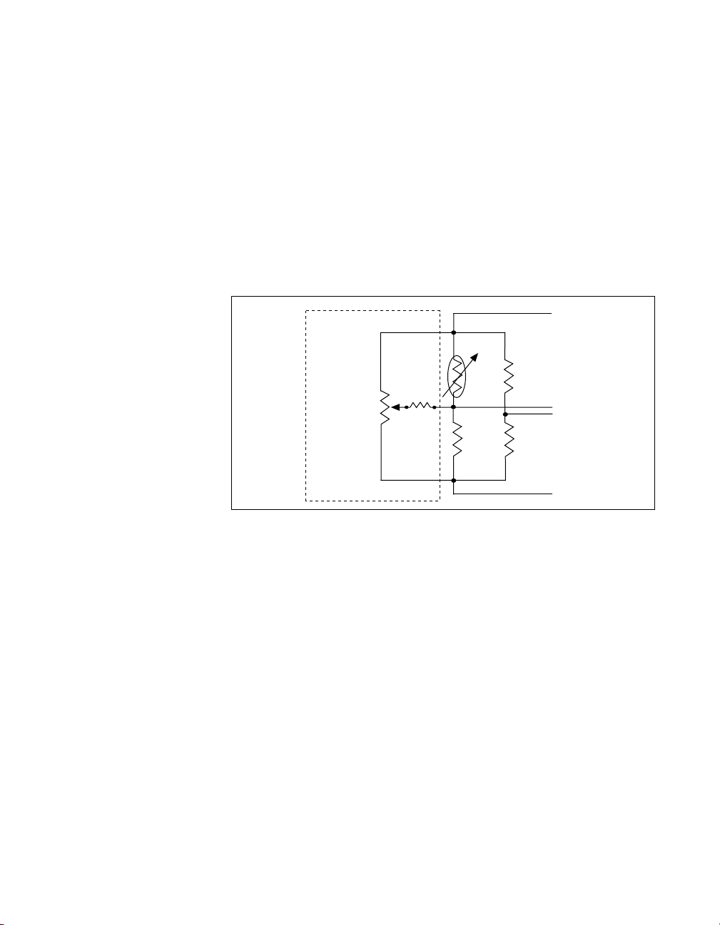
Chapter 2 Configuration and Installation
Assuming a strain-gauge range with a gauge factor of GF = 2 and a
quarter-bridge configuration, this range corresponds to ±1,498 µε as given
by the strain formula for a quarter-bridge strain-gauge configuration:
–4V
ε
-------------------------------=
GF 12Vr+()
r
where
strained voltage static unstrained voltage–
V
------------------------------------------------------------------------------------------------------- -=
r
V
exc
EX+
Trimmer
Potentiometer
SCXI-1321
R
R
null
g
R
d
R
CH+
CH–
R
EX–
Figure 2-9. Nulling Circuit
Using the SCXI-1321 with RTDs and Thermistors
When using this terminal block with RTDs or thermistor-type transducers
and with the SCXI-1121 excitation set in the Current mode, you must
disable the nulling circuit of the channel of interest. You can do this in two
steps:
1. Place the enable/disable jumper in position D (disable) as shown in
Table 2-12.
2. Remove the nulling resistor from its sockets.
© National Instruments Corporation 2-27 SCXI-1121 User Manual
Page 44

Chapter 2 Configuration and Installation
Jumper Position Description
Table 2-12. Jumper Settings of the Nulling Circuits
W1
W2
W3
W4
•
D
•
E
•
D
•
E
•
D
•
E
•
D
•
E
•
D
•
E
•
D
•
E
•
D
•
E
•
D
•
E
Nulling circuit of Channel 0 is enabled;
factory setting
Nulling circuit of Channel 0 is disabled
Nulling circuit of Channel 1 is enabled;
factory setting
Nulling circuit of Channel 1 is disabled
Nulling circuit of Channel 2 is enabled;
factory setting
Nulling circuit of Channel 2 is disabled
Nulling circuit of Channel 3 is enabled;
factory setting
Nulling circuit of Channel 3 is disabled
SCXI-1121 Shunt Calibration
Shunt calibration circuits are independent from each other but are
controlled together. In other words, when SCAL is set to 1 on the
SCXI-1121, all the shunt switches close when SCAL is cleared to 0, all the
switches open. At startup or reset, all switches are open. This shunt
calibration circuitry configuration places a shunting resistor in parallel with
the strain gauge as shown in Figure 2-10.
SCXI-1121 User Manual 2-28 www.natinst.com
Page 45

SCAL
Chapter 2 Configuration and Installation
EX+
R
g
CH+
CH–
R
EX–
SCXI-1321
R
SCAL
R
R
Figure 2-10. Shunt Circuit
The shunting resistors R
a resistor of another value to achieve the required changes. The R
are socketed so that you can replace them with
SCAL
SCAL
resistors on your terminal block have a 301 kΩ ±1% value.
Assuming a quarter-bridge strain-gauge configuration with a gauge factor
of GF = 2, the equiva lent strain change introduced by the R
SCAL
shunting
resistor is –199 µε. Determine the change as follows:
1. Determine the change caused by the shunting resistor using the
following formula:
V
change
V
excRdRSCALRg
---------------------------------------------------------- -
R
SCALRdRSCALRg
+()
+()+
V
exc
--------- -–=
2
2. Using the appropriate strain-gauge strain formula, and assuming that
you have no static voltage, determine the equivalent strain that the
R
should produce. For example, R
SCAL
= 301 kΩ and a
SCAL
quarter-bridge 120 Ω strain gauge with a gauge factor of GF = 2 and
V
= 3.333 V and R = 120 Ω produces the following result:
exc
V
= 0.3321 mV
change
Replacing the strained voltage with V
in the quarter-bridge strain
change
equation produces an equivalent –199 µε of change.
© National Instruments Corporation 2-29 SCXI-1121 User Manual
Page 46

Chapter 2 Configuration and Installation
Terminal Block Temperature Sensor
To accommodate thermocouples with the SCXI-1121, the terminal block
has an onboard temperature sensor for cold-junction compensation. You
can connect this temperature sensor in two ways:
• You can connect the temperature sensor to the MTEMP pin (C4) on the
module front connector and multiplex the sensor at the output
multiplexer along with the amplifier outputs. This is the Multiplexed
T emperature Sensor (MTS) mode. Refer to the Configuration Register
section in Chapter 4, Register Descriptions, for further details.
• You can connect the temperature sensor to a separate data acquisition
channel via MCH4± (pins 11 and 12 on the module rear signal
connector). This is the Direct Temperature Sensor (DTS) mode.
Note
Use an average of a large number of samples to obtain the most accurate reading.
Noisy environments require more samples for greater accuracy.
The SCXI-1320 and SCXI-1321 temperature sensors output 10 mV/°C and
have an accuracy of ±1 °C over the 0 to 55 °C temperature range. To
determine the temperature, use the following formulas:
where V
TEMPOUT
T °C() 100 V
T °F()
is the temperature sensor output and T (°F) and T (°C) are
()=
TEMPOUT
T °C()[]9
---------------------- - 32+=
5
the temperature readings in degrees Fahrenheit and degrees Celsius,
respectively.
The SCXI-1328 temperature sensor outputs 0.62 to 0.07 V from 0 to 55 °C
and has an accuracy of ±0.35 °C over the 15 to 35 °C range and ±0.65 °C
over the 0 to 15 °C and 35 to 55 °C ranges. To determine the temperature,
use the following formulas:
where T
T °C() T
is the temperature in kelvin
K
273.15–=
K
SCXI-1121 User Manual 2-30 www.natinst.com
Page 47

Chapter 2 Configuration and Installation
1
ln()cR
T
ln()
T
3
a = 1.288 x 10
b = 2.356 x 10
c = 9.556 x 10
T
--------------------------------------------------------------=
K
ab R
++[]
–3
–4
–8
RT = resistance of the thermistor in Ω
V
TEMPOUT
------------------------------------- -
2.5 V
–
TEMPOUT
T °C()[]9
---------------------- - 32+=
5
V
TEMPOUT
=
R
50,000
T
= output voltage of the temperature sensor
T °F()
where T (°F) and T (°C) are the temperature readings in degrees Fahrenheit
and degrees Celsius, respectively.
Terminal Block Jumper Configuration
In addition to the screw terminals, the terminal block has one jumper for
configuring the onboard temperature sensor. When you set jumper W1 on
the SCXI-1320 or SCXI-1328 (jumper W5 on the SCXI-1321) to the
MTEMP position, the jumper connects the temperature sensor output to the
SCXI-1121 output multiplexer. This is the factory setting. The DTEMP
position of jumper W1 (jumper W5 on the SCXI-1321) connects the
temperature sensor to the SCXI-1121 MCH4+ signal on the rear signal
connector.
In both MTS and DTS modes, the reference to the temperature sensor
signal is the SCXI-1121 analog ground that is connected to MCH0– in the
MTS mode and to MCH4– in the DTS mode. Notice that MCH4– is
continuously connected to the SCXI-1121 ground, whereas MCH0– is
switched through the output multiplexer.
One jumper block comprises both positions; therefore, you can use only
one type of configuration at a time. The parking position for the jumper
block is in the MTEMP position (the temperature sensor is disabled until
the RTEMP bit in the Configuration Register selects the sensor).
© National Instruments Corporation 2-31 SCXI-1121 User Manual
Page 48

Chapter 2 Configuration and Installation
Ta bles 2-13, 2-14 , and 2-15 show the jumper settings on the SCXI-1320,
SCXI-1328, and SCXI-1321 terminal blocks.
Jumper Position Description
Table 2-13. Jumper Settings on the SCXI-1320 Terminal Block
W1 MTS mode selected; factory
•
•
MTEMP
•
•
DTEMP
setting; parking position
W1 DTS mode selected
•
•
MTEMP
•
•
DTEMP
Table 2-14. Jumper Settings on the SCXI-1328 Terminal Block
Jumper Position Description
W1 MTS mode selected; factory
DTEMP MTEMP
•••
•
setting; parking position
W1 DTS mode selected
DTEMP MTEMP
Table 2-15. Jumper Settings on the SCXI-1321 Terminal Block
•••
•
Jumper Position Description
W5 MTS mode selected;
MTEMP
•••
•
DTEMP
factory setting; parking
position
W5 DTS mode selected
•••
•
MTEMP
SCXI-1121 User Manual 2-32 www.natinst.com
DTEMP
Page 49

Terminal Block Signal Connection
Chapter 2 Configuration and Installation
Warnings
The chassis GND terminals on your terminal block are for grounding high
impedance sources such as a floating source (1 mA maximum). Do not use these terminals
as safety earth grounds.
If high voltages (≥42 V
) are present, you must connect the safety earth ground to the
rms
strain-relief tab. This complies with UL 1244 and fully protects against electric shock when
the terminal block is not connected to the chassis. To connect the safety earth ground to the
strain-relief tab, run an earth ground wire in the cable from the signal source to the terminal
block. National Instruments is not liable for any damages or injuries resulting from
inadequate safety earth ground connections.
Shock Hazard—This unit should only be opened by qualified personnel aware of the
dangers involved. Disconnect all power before removing cover. Always install grounding
screw.
To conn ect the signal to the terminal block, use the following procedure:
1. Remove the grounding screw of the top cover.
2. Snap out the top cover of the shield by placing a screwdriver in the
groove at the bottom of the terminal block.
3. Slide the signal wires, one at a time, through the front panel
strain-relief opening. You can add padding or insulation if necessary.
4. Connect the wires to the screw terminals. For thermistor and RTD
connection, follow the procedure stated in the Using the SCXI-1321
with RTDs and Thermistors section earlier in this chapter.
5. Tighten the larger strain-relief screws.
6. Snap the top cover back in place.
7. Reinsert the grounding screw to ensure proper shielding.
8. Connect the terminal block to the SCXI-1121 front connector as
explained in the Terminal Block Installation section later in this
chapter.
Figure 2-11 shows a parts locator diagram for the SCXI-1320 terminal
block. Figure 2-12 shows a parts locator diagram for the SCXI-1328
terminal block. Figure 2-13 shows a parts locator diagram for the
SCXI-1321 terminal block.
© National Instruments Corporation 2-33 SCXI-1121 User Manual
Page 50
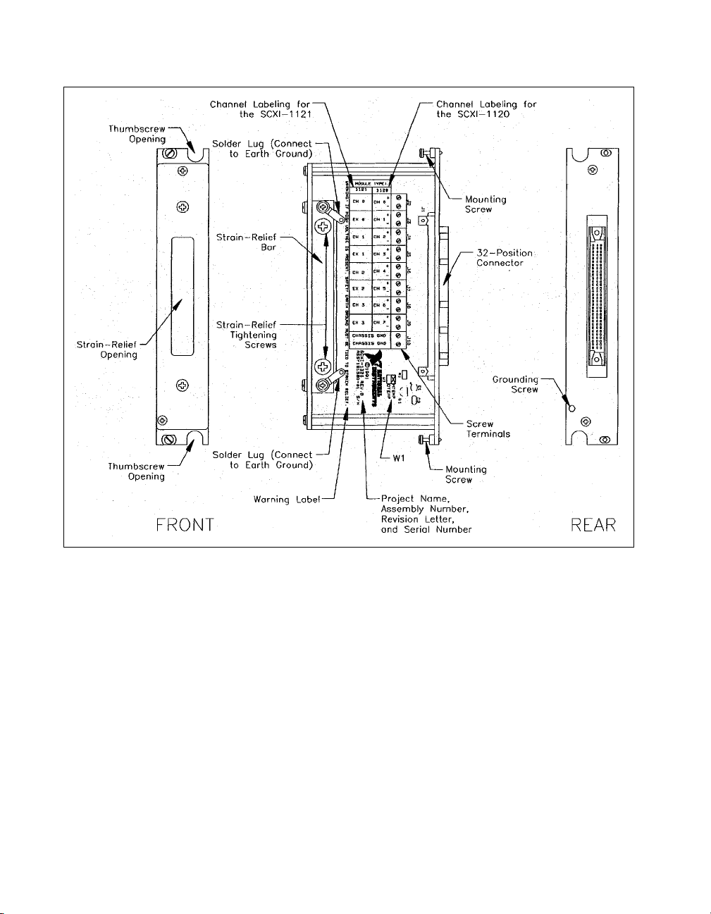
Chapter 2 Configuration and Installation
Figure 2-11. SCXI-1320 Parts Locator Diagram
SCXI-1121 User Manual 2-34 www.natinst.com
Page 51

Chapter 2 Configuration and Installation
Figure 2-12. SCXI-1328 Parts Locator Diagram
© National Instruments Corporation 2-35 SCXI-1121 User Manual
Page 52

Chapter 2 Configuration and Installation
Figure 2-13. SCXI-1321 Parts Locator Diagram
Terminal Block Installation
To connect the terminal block to the SCXI-1121 front connector, perform
the following steps:
1. Connect the SCXI-1121 front connector to its mating connector on the
terminal block.
2. Make sure that the SCXI-1121 top and bottom thumbscrews do not
obstruct the rear panel of the terminal block.
3. Tighten the top and bottom screws on the back of the terminal block to
hold it securely in place.
SCXI-1121 User Manual 2-36 www.natinst.com
Page 53

Rear Signal Connector
Note
If you are using the SCXI-1121 with a National Instruments data acquisition board
and cable assembly , you do not need to read the remainder of this chapter . If you are using
the SCXI-1180 feedthrough panel, the SCXI-1343 rear screw terminal adapter, or the
SCXI-1351 one-slot cable extender with the SCXI-1121, you should read this section.
Figure 2-14 shows the pin assignments for the SCXI-1121 rear signal
connector.
Chapter 2 Configuration and Installation
AOGND
MCH0+
MCH1+
MCH2+
MCH3+
MCH4+
OUTREF
SERDATIN
DAQD*/A
SLOT0SEL*
DIG GND
SERCLK
RSVD
12
34
56
78
910
11 12
13 14
15 16
17 18
19 20
21 22
23 24
25 26
27 28
29 30
31 32
33 34
35 36
37 38
39 40
41 42
43 44
45 46
47 48
49 50
AOGND
MCH0–
MCH1–
MCH2–
MCH3–
MCH4–
DIG GND
SERDATOUT
SCANCLK
Figure 2-14.
© National Instruments Corporation 2-37 SCXI-1121 User Manual
SCXI-1121 Rear Signal Connector Pin Assignment
Page 54

Chapter 2 Configuration and Installation
Rear Signal Connector Signal Descriptions
Pin Signal Name Description
1-2 AOGND Analog Output Ground—These pins are connected to the analog
reference when jumper W33 is in position AB-R0.
3-12 MCH0± through
MCH4±
Analog Output Channels 0 through 4—Connects to the data
acquisition board differential analog input channels.
19 OUTREF Output Reference—This pin serves as the reference node for the
analog channels output in the Pseudodifferential Reference mode.
It should be connected to the analog input sense of the NRSE data
acquisition board.
24, 33 DIG GND Digital Ground—These pins supply the reference for data
acquisition board digital signals and are tied to the module digital
ground.
25 SERDATIN Serial Data In—This signal taps into the SCXIbus MOSI line to
provide serial input data to a module or Slot 0.
26 SERDATOUT Serial Data Out—This signal taps into the SCXIbus MISO line to
accept serial output data from a module.
27 DAQD*/A Data Acquisition Board Data/Address Line—This signal taps into
the SCXIbus D*/A line to indicate to the module whether the
incoming serial stream is data or address information.
29 SLOT0SEL* Slot 0 Select—This signal taps into the SCXIbus INTR* line to
indicate whether the information on MOSI is being sent to a
module or Slot 0.
36 SCANCLK Scan Clock—This indicates to the SCXI-1121 that a sample has
been taken by the data acquisition board and causes the SCXI-1121
to change channels. See the Timing Requirements and
Communication Protocol section later in this chapter for more
detailed information on timing.
37 SERCLK Serial Clock—This signal taps into the SCXIbus SPICLK line to
clock the data on the MOSI and MISO lines. See the Timing
Requirements and Communication Protocol section later in this
chapter for more detailed information on timing.
43 RSVD Reserved.
All other pins are not connected.
SCXI-1121 User Manual 2-38 www.natinst.com
Page 55

Chapter 2 Configuration and Installation
The signals on the rear signal connector can be classified as analog output
signals, digital I/O signals, or timing I/O signals. Signal connection
guidelines for each of these groups are given in the following section.
Analog Output Signal Connections
Pins 1 through 12 and pin 19 of the rear signal connector are analog output
signal pins. Pins 1 and 2 are AOGND signal pins. AOGND is an analog
output common signal that is routed through jumper W33 to the analog
reference on the SCXI-1121. You can use these pins for a general analog
power ground tie point to the SCXI-1121 if necessary. In particular, when
using differential input data acquisition boards such as the MIO-16 series,
it is preferable to leave jumper W33 in its factory setting or in position
AB-R1 to avoid ground loops. With data acquisition boards that are
configured for referenced single-ended (RSE) measurements, W33 should
be in position AB-R0 to connect the SCXI-1121 ground to the data
acquisition analog ground. Pin 19 is the OUTREF pin this pin is connected
internally to the analog reference when jumper W33 is in position AB-R2.
Pins 3 through 12 are the analog output channels of the SCXI-1121. Pins 3
and 4 or MCH0± are a multiplexed output of all four input channels and the
temperature sensor output. Pins 5 through 10 or MCH1± through MCH3±
are a parallel connection of input channels 1 through 3 to the rear signal
connector. Pins 11 and 12 or MCH4± are a direct connection of the
temperature sensor. Notice that the temperature sensor is located on the
terminal block. For further details on configuring the temperature sensor
output, refer to the SCXI-1320, SCXI-1328, and SCXI-1321
Terminal Blocks section earlier in this chapter.
Warning
The SCXI-1121 analog outputs are not overv oltage-protected. Applying external
voltages to these outputs can damage the SCXI-1121. National Instruments is not liable for
any damages resulting from such signal connections.
Note
The SCXI-1121 analog outputs are short-circuit protected.
© National Instruments Corporation 2-39 SCXI-1121 User Manual
Page 56

Chapter 2 Configuration and Installation
Digital I/O Signal Connections
Pins 24 through 27, 29, 33, 36, 37, and 43 constitute the digital I/O lines of
the rear signal connector. They are divided into three categories—the
digital input signals, the digital output signals, and the digital timing
signals.
The digital input signals are pins 24, 25, 27, 29, 33, and 37. The data
acquisition board uses these pins to configure an SCXI module that is under
data acquisition board control. Each digital line emulates the SCXIbus
communication signals as follows:
• Pin 25 is SERDATIN and is equivalent to the SCXIbus MOSI serial
data input line.
• Pin 27 is DAQD*/A and is equivalent to the SCXIbus D*/A line. It
indicates to the module whether the incoming serial stream on
SERDATIN is data (DAQD*/A = 0), or address (DAQD*/A = 1)
information.
• Pin 29 is SLO T0SEL* and is equi va lent to the SCXIbus INTR* line. It
indicates whether the data on the SERDATIN line is being sent to
Slot 0 (SLOT0SEL* = 0) or to a module (SLOT0SEL* = 1).
• Pins 24 and 33 are the digital ground references for the data acquisition
board digital signals and are tied to the module digital ground.
• P in 37 is SERCLK and is equiv alent to the SCXIb us SPICLK line and
is used to clock the serial data on the SERDATIN line into the module
registers.
The digital output signal is pin 26.
• Pin 26 is SERDATOUT and is equivalent to SCXIbus MISO when
jumper W38 is in position 1.
The digital input and output signals of the SCXI-1121 match the digital I/O
lines of the MIO-16 board. When used with an SCXI-1341, SCXI-1342, or
SCXI-1344 cable assembly, the SCXI-1121 signals match the digital lines
of the Lab-NB/Lab-PC/Lab-PC+/Lab-LC boards and the PC-LPM-16
board, respectively. Table 2-16 lists the equivalences. For more
information, consult Appendix E, SCXI-1121 Cabling.
SCXI-1121 User Manual 2-40 www.natinst.com
Page 57

Chapter 2 Configuration and Installation
Table 2-16. SCXIbus to SCXI-1121 Rear Signal Connector to Data Acquisition Board Pin Equivalences
SCXI-1121
SCXIbus Line
Rear Signal
Connector
MIO-16
Lab-NB/Lab-PC
Lab-PC+/Lab-LC
PC-LPM-16
MOSI SERDATIN ADIO0 PB4 DOUT4
D*/A DAQD*/A ADIO1 PB5 DOUT5
INTR* SLOT0SEL* ADIO2 PB6 DOUT6
SPICLK SERCLK EXTSTROBE* PB7 DOUT7
MISO SERDATOUT BDIO0 PC1 DIN6
The digital timing signals are pins 36 and 43.
• Pin 36 is used as a clock by the SCXI-1121 to increment the
MUXCOUNTER after each conversion by the data acquisition board
during scanning. This signal is referred to as SCANCLK. See
Chapter 3, Theory of Operation, for a description of MUXCOUNTER.
• Pin 43 is a reserved digital input.
The following specifications and ratings apply to the digital I/O lines.
Absolute maximum voltage
Input rating 5.5 V with respect to DIG GND
Digital input specifications (referenced to DIG GND):
V
input logic high voltage 2 V minimum
IH
V
input logic low voltage 0.8 V maximum
IL
I
input current leakage ±1 µA maximum
I
Digital output specifications (referenced to DIG GND):
V
output logic high voltage 3.7 V minimum at 4 mA maximum
OH
V
output logic low voltage 0.4 V maximum at 4 mA maximum
OL
© National Instruments Corporation 2-41 SCXI-1121 User Manual
Page 58

Chapter 2 Configuration and Installation
Timing Requirements and Communication Protocol
Timing Signal
The data acquisition timing signal is SCANCLK.
SCANCLK is used to increment MUXCOUNTER on its rising edge.
Figure2-15 shows the timing requirements of the SCANCLK signal. These
requirements will ensure that SCANCLK is properly transmitted over
TRIG0.
SCANCLK
T
T
low
high
T
low
T
high
Time low before rising edge 400 nsec minimum
Time high before falling edge 250 nsec minimum
Figure 2-15.
SCANCLK Timing Requirements
For output selection time specifications, refer to AppendixA,
Specifications.
Communication Signals
This section describes the methods for communicating on the Serial
Peripheral Interface (SPI) bus and their timing requirements. The
communication signals are SERDATIN, DAQD*/A, SLOT0SEL*,
SERDATOUT, and SERCLK. Furthermore, SS* is produced by Slot 0
according to data acquisition board programming, and SS* timing
relationships will also be discussed. For information on the Slot 0
Slot-Select Register, consult Chapter 4, Register Descriptions.
The data acquisition board determines to which slot it will talk by writing
a slot-select number to Slot 0. In the case of an SCXI-1001 chassis, this
write also determines to which chassis the data acquisition board will talk.
Writing a slot-select number is also used in programming the Slot 0
hardscan circuitry. See Chapter 5, Programming, for information on
programming the Slot 0 hardscan circuitry.
The following sections detail the procedure for selecting a slot in a
particular chassis. Figure2-16 illustrates the timing of this procedure with
the example case of selecting Slot 11 in Chassis 9. Notice that the
factory-default chassis address for the SCXI-1000 is address 0. For
information on changing the address of your chassis, consult the
SCXI-1000/1001 User Manual. An SCXI-1000 chassis will respond to any
chassis number.
SCXI-1121 User Manual 2-42 www.natinst.com
Page 59
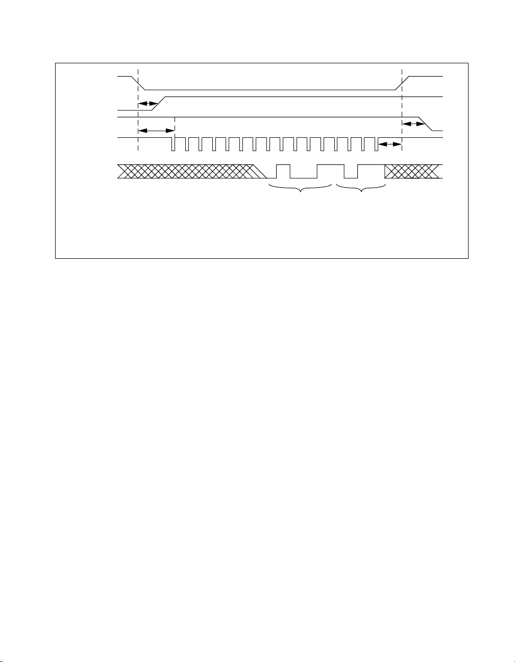
SLOT0SEL*
SS*X
Chassis Y
SS*11
Chassis 9
SERCLK
SERDATIN
T
T
ss_dis
clk_wait
Chapter 2 Configuration and Installation
T
slot0sel*_wait
0100 110 11
Chassis ID = 9 Slot 11
T
ss_en
T
ss _ dis
T
clk _ wait
T
slot0sel* _ wait
T
ss _ en
SLOT0SEL* low to SS* disabled 200 nsec maximum
SLOT0SEL* low to first rising edge on SERCLK 75 nsec minimum
Last rising edge on SERCLK to SLOT0SEL* high 250 nsec minimum
SLOT0SEL* high to SS* enabled 350 nsec maximum
Figure 2-16. Slot-Select Timing Diagram
To write the 16 -bit slot-select number to Slot 0, follow these steps:
1. Initial conditions:
SERDATIN = don't care
DAQD*/A = don't care
SLOT0SEL* = 1
SERCLK = 1
2. Clear SLOT0SEL* to 0. This will deassert all SS* lines to all modules
in all chassis.
3. For each bit, starting with the most significant bit, perform the
following action:
a. SERDATIN = bit to be sent. These bits are the data that is being
written to the Slot-Select Register.
b. SERCLK = 0
c. SERCLK = 1. This rising edge clocks the data.
4. Set SLOT0SEL* to 1. This will assert the SS* line of the module
whose slot number was written to Slot 0. If multiple chassis are being
used, only the appropriate slot in the chassis whose address
corresponds to the written chassis number will be selected. When no
communication is taking place between the data acquisition board and
any modules, it is recommended that 0 be written to the Slot-Select
Register to ensure that no accidental writes occur.
© National Instruments Corporation 2-43 SCXI-1121 User Manual
Page 60

Chapter 2 Configuration and Installation
Figure 2-17 shows the timing requirements on the SERCLK and
SERDATIN signals. You must observe these timing requirements for all
communications. T
SERCLK
SERDATIN
SERDATOUT
T
delay
is a specification of the SCXI-1121.
delay
T
T
low
T
setup
high
T
hold
T
T
T
T
T
low
high
setup
hold
delay
Minimum low time 65 nsec minimum
Minimum high time 400 nsec minimum
SERDATIN setup time 200 nsec minimum
SERDATIN hold time 200 nsec minimum
SERDATOUT delay 350 nsec maximum
Figure 2-17. Serial Data Timing Diagram
After the Slot-Select line to an SCXI-1121 has been asserted, you can write
to its Configuration Register and read from its Module ID Register by
following the protocols given below. The contents of the Module ID
Register are reinitialized by deasserting Slot-Select. After the 32 bits of
data are read from the Module ID Register, further data will be zeros until
reinitialization occurs.
To write to the Configuration Register, follow these steps:
1. Initial conditions:
SS* asserted low
SERDATIN = don't care
DAQD*/A = 0 (indicates data will be written to Configuration
Register)
SLOT0SEL* = 1
SERCLK = 1 (and has not transitioned since SS* went low)
2. For each bit to be written:
Establish the desired SERDATIN level corresponding to this bit.
SERCLK = 0
SERCLK = 1. Clock the data.
SCXI-1121 User Manual 2-44 www.natinst.com
Page 61

Chapter 2 Configuration and Installation
3. Pull SLOT0SEL* low to deassert the SS* line and establish conditions
for writing a new slot-select number to the Slot 0 Slot-Select Register.
4. If you are not selecting another slot, you should write zero to the Slot
0 Slot-Select Register.
Figure 2-18 illustrates a write to the SCXI-1121 Configuration Register of
the binary pattern:
10000011 00001111
SLOT0SEL*
SS*
SERCLK
SERDATIN
Figure 2-18. Configuration Register Write Timing Diagram
01 00001100001111
To read from the Module ID Register, follow these steps:
1. Initial conditions:
SS* asserted low
SERDATIN = don't care
DAQD*/A = 1. Make sure DAQD*/A does not go low or erroneous
data will be written to the Configuration Register.
SLOT0SEL* = 1
SERCLK = 1 (and has not changed since SS* went low)
2. For each bit to be read:
SERCLK = 0
SERCLK = 1. Clock the data.
Read the level of the SERDATOUT line.
3. Pull SLOT0SEL* low to deassert the SS* line and establish conditions
for writing a new slot- select number to the Slot 0 Slot-Select Register.
4. If you are not selecting another slot, you should write zero to the Slot 0
Slot-Select Register.
© National Instruments Corporation 2-45 SCXI-1121 User Manual
Page 62

Chapter 2 Configuration and Installation
Figure 2-19 illustrates a read of the SCXI-1121 Module ID Register.
SLOT0SEL*
SS*
SERCLK
SERDATOUT
T
delay
000000 00000000000000000000000001
byte 0 = 2 byte 3 = 0byte 2 = 0byte 1 = 0
For further details on programming these signals, refer to Chapter 5,
Programming.
T
delay
SS* high to SERDATOUT high 350 nsec maximum
Figure 2-19. SCXI-1121 Module ID Register Timing Diagram
SCXI-1121 User Manual 2-46 www.natinst.com
Page 63

Theory of Operation
This chapter contains a functional overview of the SCXI-1121 module and
explains the operation of each functional unit making up the SCXI-1121.
Functional Overview
The block diagram in Figure 3-1 illustrates the key functional components
of the SCXI-1121.
3
SCXIbus
Isolated Section
+
–
+
–
Front Connector
+
–
+
+
–
•
•
•
•
+
+
–
Nonisolated
Section
Input channel 0
Excitation 0
Input channel 3
Excitation 3
Temperature sensor
Figure 3-1.
Digital
Interface
and
Control
•
•
•
•
SCXI-1121 Block Diagram
Timing
and
Analog
Output
Stage
Rear Signal Connector
© National Instruments Corporation 3-1 SCXI-1121 User Manual
Page 64

Chapter 3 Theory of Operation
The major components of the SCXI-1121 are as follows:
• SCXIbus connector
• Digital interface
• Digital control circuitry
• Timing and analog circuitry
The SCXI-1121 consists of four isolated amplifier channels with gains of
1, 2, 5, 10, 20, 50, 100, 200, 500, 1,000, and 2,000, and four isolated
excitation channels with voltage or current excitation. The SCXI-1121 also
has a digital section for automatic control of channel scanning, for
temperature selection, and for MUXCOUNTER clock selection.
The theory of operation for each of these components is explained in the
rest of this chapter.
SCXI-1121 User Manual 3-2 www.natinst.com
Page 65

SCXIbus Connector
Chapter 3 Theory of Operation
Figure 3-2 shows the pin assignments for the SCXIbus connector.
GUARD
GUARD
GUARD
AB0+
GUARD
GUARD
GUARD
GUARD
GUARD
GUARD
RESET*
MISO
V–
V–
CHSGND
CHSGND
V+
V+
+5 V
SPICLK
TRIG0
SS*
A1
B1
A2
B2
A3
B3
A4
B4
A5
B5
A6
B6
A7
B7
A8
B8
A9
B9
A10
B10
A11
B11
A12
B12
A13
B13
A14
B14
A15
B15
A16
B16
A17
B17
A18
B18
A19
B19
A20
B20
A21
B21
A22
B22
A23
B23
A24
B24
D1
C1
D2
C2
D3
C3
D4
C4
D5
C5
D6
C6
D7
C7
D8
C8
D9
C9
D10
C10
D11
C11
D12
C12
D13
C13
D14
C14
D15
C15
D16
C16
D17
C17
D18
C18
D19
C19
D20
C20
D21
C21
D22
C22
D23
C23
D24
C24
GUARD
GUARD
GUARD
AB0–
GUARD
GUARD
GUARD
GUARD
GUARD
GUARD
CHSGND
CHSGND
CHSGND
CHSGND
CHSGND
RSVD
INTR*
D*/A
V–
V–
CHSGND
CHSGND
V+
V+
+5 V
MOSI
SCANCON
Figure 3-2.
SCXIbus Connector Pin Assignment
© National Instruments Corporation 3-3 SCXI-1121 User Manual
Page 66

Chapter 3 Theory of Operation
SCXIbus Connector Signal Descriptions
Pin Signal Name Description
A1, B1, C1, D1, A2,
D2,A3, B3, C3, D3, A4,
D4, A5, B5, C5, D5, A6, D6
B2 AB0+ Analog Bus 0+ —Positive analog bus 0 line. Used
C2 AB0– Analog Bus 0– —Negative analog b us 0 line. Used
C13-C17, A21, B21, C21,
D21
C18 RSVD Reserved.
A19 RESET* Reset—When pulled low, reinitializes the module
B19 MISO Master-In Slave-Out—Transmits data from the
C19 D*/A Data/Address—Indicates to the module whether
D19 INTR* Interrupt—Active low. Causes data that is on
GUARD Guard—Shields and guards the analog bus lines
from noise.
to multiplex several modules to one analog signal.
to multiplex several modules to one analog signal.
CHSGND Chassis Ground—Digital and analog ground
reference.
to its power-up state. Totem pole. Input.
module to the SCXIbus. Open collector. I/O.
address information or data information is being
sent to the module on MOSI. Open collector. I/O.
MOSI to be written to the Slot-Select Register in
Slot 0. Open collector. Output.
A20, B20, C20, D20 V– Negative Analog Supply— –18.5 to –25 V.
A22, B22, C22, D22 V+ Positive Analog Supply— +18.5 to +25 V.
A23, D23 +5 V +5 VDC Source—Digital power supply.
B23 SPICLK Serial Peripheral Interface (SPI) Clock—Clocks
the serial data on the MOSI and MISO lines. Open
collector. I/O.
C23 MOSI Master-Out Slave-In—Transmits data from the
SCXIbus to the module. Open collector. I/O.
SCXI-1121 User Manual 3-4 www.natinst.com
Page 67

Chapter 3 Theory of Operation
Pin Signal Name Description
A24 TRIG0 TRIG0—General-purpose trigger line used by the
SCXI-1121 to send SCANCLK to other modules
or receive SCANCLK from other modules. Open
collector. I/O.
B24 SS* Slot Select—When low, enables module
communications over the SCXIbus. Totem pole.
Input.
C24 SCANCON Scanning Control—Combination output enable
and reload signal for scanning operations. Totem
pole. Input.
All other pins are not connected.
MOSI, MISO, SPICLK, and SS* form a synchronous communication link
that conforms with SPI using an idle-high clock and second-edge data
latching. D*/A, INTR*, and RESET* are additional control signals.
When the module is being used in an SCXI-1000 or SCXI-1001 chassis, the
data acquisition board, via the module rear signal connector, must tap into
the open-collector backplane signal lines as a master to write to the module.
The signal connections from the rear signal connector to the backplane are
shown in Table 3-1.
Table 3-1. SCXIbus Equivalents for the Rear Signal Connector
Rear Signal
Connector Signal
SCXIbus Equivalent
SERDATIN MOSI
DAQD*/A D*/A
SLOT0SEL* INTR* Jumper W44 must be set to position 1
SERCLK SPICLK
SERDATOUT MISO Jumper W38 must be set to position 1
The SCXI-1121 module converts the data acquisition board signals to
open-collector signals on the backplane of the SCXI chassis. In order for
the data acquisition board to talk to a slot, the board must first assert the SS*
for that slot. This is done by asserting INTR* low, writing a 16-bit number
over MOSI corresponding to the desired slot (and chassis if an SCXI-1001
© National Instruments Corporation 3-5 SCXI-1121 User Manual
Page 68
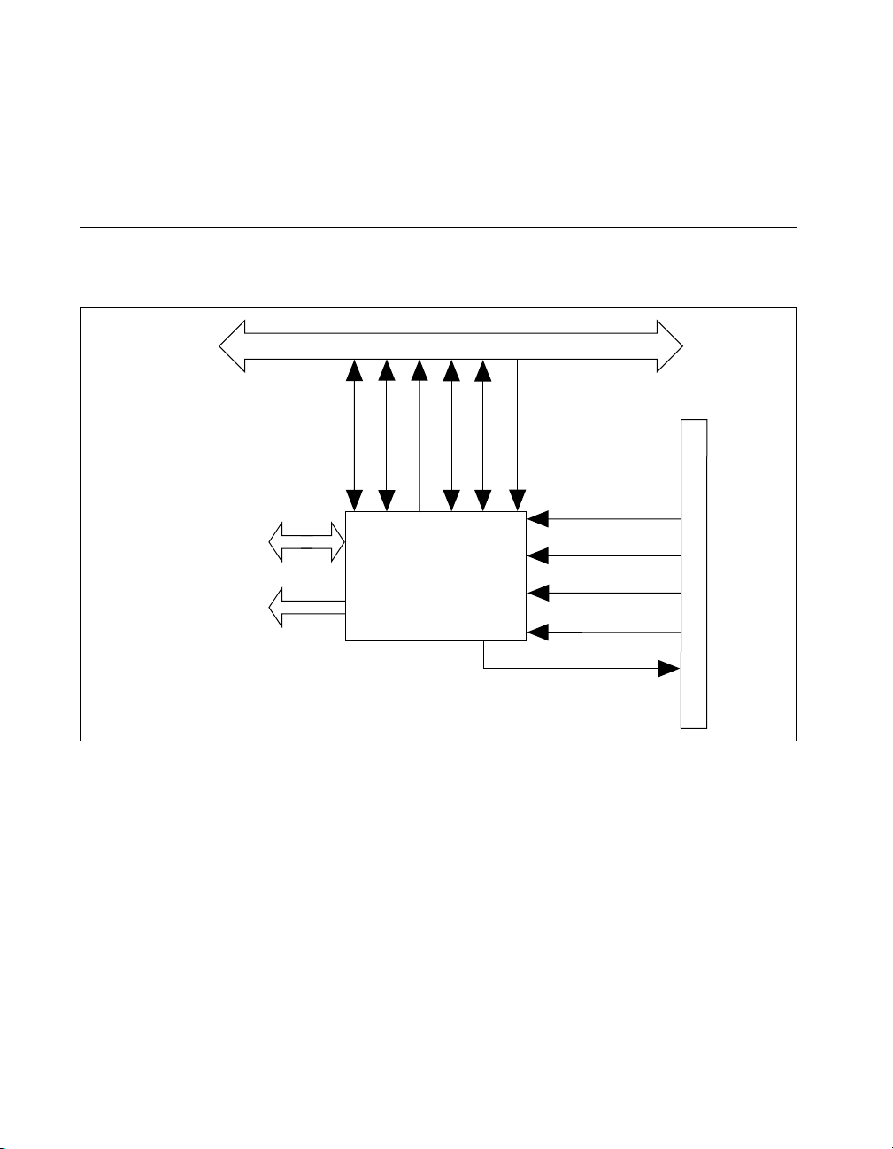
Chapter 3 Theory of Operation
chassis is being used), and then releasing INTR* high. At this point, SS* of
the desired slot is asserted low and the data acquisition board can
communicate with the module in that slot according to the SPI protocol.
Digital Interface
Figure 3-3 shows a diagram of the SCXI-1121 and SCXIbus digital
interface circuitry.
Buffered Serial
Data
Buffered Digital
Signal Controls
MISO
SCXIbus
INTR*
SPICLK
Digital
Interface
D*/A
MOSI
SS*
SERDATIN
DAQD*/A
SLOT0SEL*
SERCLK
Rear Signal Connector
SERDATOUT
Figure 3-3.
Digital Interface Circuitry Block Diagram
The digital interface circuitry is divided into a data acquisition section
and an SCXIbus section. The SCXI-1121 connects to the SCXIbus via a
4 × 24 metral receptacle and to the data acquisition board via a 50-pin
ribbon-cable header. The digital interface circuitry buffers the digital
signals from the data acquisition board and from the SCXIbus and sends
signals back and forth between the data acquisition board and the SCXIbus.
SCXI-1121 User Manual 3-6 www.natinst.com
Page 69

Digital Control Circuitry
Figure 3-4 diagrams the SCXI-1121 digital control.
Chapter 3 Theory of Operation
Serial Data Out
Input Channel
Select
Module ID Register
Buffered
Configuration
Register
Output
Stage
Control
Figure 3-4.
SCANCLK
Path
Control
Hardware
Scan
Control
SCXI-1121 Digital Control
Serial Data In
Buffered Digital
Control Signals
The digital control section consists of the Configuration Register and the
Module ID Register.
The Configuration Register is a two-byte, serial-in parallel-out shift
register. Data is received on the MOSI line from either Slot 0 or the data
acquisition board when SS* is enabled and D*/A indicates data transfer
(D*/A low). The Configuration Register provides temperature channel
selection and channel selection, and configures the SCXI-1121 for
scanning options. All the control bits are fed into a latch before being
routed to the rest of the module. The channel-select bits are taken directly
from the shift register. Complete descriptions of the register bits are given
in Chapter 4, Register Descriptions. Writes to the Configuration Register
require the following steps:
1. SS* goes low, enabling communication with the board.
2. D*/A goes low, indicating that the information sent on the MOSI line
is data.
© National Instruments Corporation 3-7 SCXI-1121 User Manual
Page 70

Chapter 3 Theory of Operation
3. The serial data is available on MOSI and SPICLK clocks it into the
register.
4. SS* goes high and D*/A goes high, indicating an end of
communication. This action latches the Configuration Register bits.
When the SCXIbus is reset, all bits in the Configuration Register are
cleared.
The Module ID Register connects to MISO on the SCXIbus. The Module
ID Register is an 8-bit parallel/serial-in serial-out shift register and an SPI
communication adapter. The contents of the Module ID Register are written
onto MISO during the first four bytes of transfer after SS* has been asserted
low. Zeros are written to MISO thereafter until SS* is released and
reasserted. The SCXI-1121 module ID is hex 00000002.
Analog and Timing Circuitry
The SCXIbus provides analog power (±18.5 VDC) that is regulated on the
SCXI-1121 to ±15 VDC, a guard, an analog bus (AB0±), and a chassis
ground (CHSGND). AB0± buses the SCXI-1121 output to other modules
or receives outputs from other modules via the SCXIbus. Refer to the
Calibration section later in this chapter for more information. The guard
guards the analog bus, and can be connected via jumper W33 to the analog
ground reference or can be left floating (a connection can be made by
another board).
The data acquisition board analog input and timing is the interface between
the SCXI-1121 output and the data acquisition board. This is fully
described in the following section.
Analog Input Channels
Figure 3-5 is a diagram of the analog input block.
SCXI-1121 User Manual 3-8 www.natinst.com
Page 71
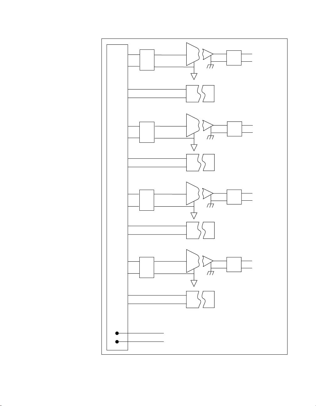
Chapter 3 Theory of Operation
Input Channel 0
+
–
LPF
+
I
LPF
To Output
+
–
Stage
+
–
EX0
Input Channel 1
+
–
LPF
+
–
+
EX1
LPF
I
To Output
+
–
Stage
Input Channel 2
+
–
LPF
+
–
+
EX2
LPF
I
To Output
+
–
Stage
Input Channel 3
+
–
LPF
+
LPF
To Output
+
–
Stage
I
+
–
EX3
MTEMP
DTEMP
Figure 3-5. Analog Input Block Diagram
© National Instruments Corporation 3-9 SCXI-1121 User Manual
Page 72

Chapter 3 Theory of Operation
The analog input consists of four isolated single-ended noninverting
amplifiers. In addition, lowpass filtering is available at the inputs. You can
jumper select one of two bandwidths, 10 kHz or 4 Hz. The amplifier gain
is divided into two stages, a first stage providing gains of 1, 10, 50, and 100,
and a second stage providing gains of 1, 2, 5, 10, and 20. Also, the module
has an internal completion network that can be used with half-bridge or
quarter-bridge networks. Each channel is configurable to a diff erent
bandwidth, gain, or completion network operation.
Use the following formula to determine the overall gain of a gi ven amplifier
input channel:
where G
G
is the overall gain and G
total
total
G
×=
1stG2nd
and G
1st
are the first and
2nd
second-stage gains. It is important to note that the choice of gain in each
stage will affect the amplifier ba ndwidth. To determine the bandwidth of a
given gain stage use the following formula:
BW
GBWP
-----------------=
G
where BW is a given amplifier stage bandwidth, GBWP is the gain
bandwidth product (typically 800 kHz), and G is the gain at this stage. This
BW might be of concern at high first-stage gains such as 50 and 100. In this
case the first-stage amplifier has a BW equal to 16 kHz and 8 kHz,
respectively. Because of this decrease in the amplifier bandwidth, the
channel overall bandwidth decreases, but noise immunity improv es. If this
bandwidth limitation is unacceptable, you should spread the gains over
both stages, thus increasing the BW of each amplifier stage. In most cases
this will introduce a negligible effect on the channel bandwidth. For
example, to achiev e a gain of 100, use G
1,000 use G
= 50 and G
1st
2nd
= 20.
All the amplifier input channels are overvoltage-protected to 240 V
= 10 and G
1st
= 10 for a gain of
2nd
rms
with
power on or off.
The isolated amplifiers fulfill two purposes on the SCXI-1121 module.
They convert a small signal riding on a high common-mode voltage into a
single-ended signal with respect to the SCXI-1121 chassis ground. With
this conversion, the input analog signal can be extracted from a high
common-mode voltage or noise before being sampled and conv erted by the
data acquisition board. The isolated amplifier also amplifies and conditions
an input signal, which results in an increase in measurement resolution and
accuracy .
SCXI-1121 User Manual 3-10 www.natinst.com
Page 73

After isolation, further filtering is available to increase the noise immunity
of the amplifier channel. It is important to note that the overall amplifier
bandwidth is determined by both filtering stages, so to achieve the required
bandwidth, both filtering sections should be set the same, as indicated in
Chapter 2, Configuration and Installation.
Excitation Output Channels
In addition to the four input channels, the SCXI-1121 contains four fully
isolated excitation channels, each corresponding to an input channel. For
instance, input channel 0 corresponds to excitation channel 0. Each
excitation channel consists of a voltage/current source with overvoltage
protection and current limiting. Two levels of excitation are available for
each mode of operation. In the voltage mode you can set the level to
3.333V or 10 V in the current mode you can set the level to 150 µA or
450µA. You can choose one configuration out of the four available. To
configure the excitation channels refer to Chapter 2, Configuration and
Installation. The excitation channels are isolated from each other and are
independently configurable for voltage or current excitation.
Calibration
Chapter 3 Theory of Operation
Calibration Equipment Requirements
For best measurement results, calibrate the SCXI-1121 so that its offset is
adjusted to 0 ± 3 mV RTO and 0 ± 6 µV RTI and its excitation output is
adjusted to ±0.04%. According to standard practice, the equipment used to
calibrate the SCXI-1121 should be 10 times as accurate as the SCXI-1121,
that is, have 0.004% rated accuracy. Practically speaking, calibration
equipment with four times the accuracy of the item under calibration is
generally considered acceptable. Four times the SCXI-1121 accuracy is
0.016%. To calibrate the SCXI-1121 you need the following equipment:
• For the excitation channels, you need a voltmeter with the following
specifications:
– Accuracy:±0.004% standard
±0.016% sufficient
– Range: 0 to +5 V for 3.333 V and greater than +10 V for 10 V
– Resolution:5 1/2 digits
© National Instruments Corporation 3-11 SCXI-1121 User Manual
Page 74

Chapter 3 Theory of Operation
• You also need a 120 Ω 1/4 W precision resistor with tempco less than
or equal to 5 ppm, or an ammeter with the following specifications:
– Accuracy: ±0.004% standard
±0.016% sufficient
– Range: 0.5 mA
– Resolution: 6 1/2 digits
• I f you use the resistor to calibrate the current e xcitation, you also need
an ohmmeter with four-wire measurement and the following
specifications:
– Accuracy: ±0.004% standard
±0.016% sufficient
– Range: 200 Ω
– Resolution: 5 1/2 digits
A multiranging 5 1/2-digit digital multimeter can provide you with most of
the necessary functions described previously. We will refer to the
measuring instrument as a digital multimeter (DMM).
Each channel on the SCXI-1121 has two potentiometers dedicated for
calibration. For the amplifier channels, one potentiometer is used to null the
output offset; the other is used to null the input offset. On the excitation
channels, one potentiometer is used to adjust the voltage reference, while
the other is used to adjust the current source.
Offset Null Adjust
Follow these steps to null the offset of the amplifier channels:
1. Short the inputs of the DMM together and then connect them to chassis
ground.
2. Record the measurement indicated by the DMM display. This is the
DMM inherent offset and should be subtracted from subsequent
measurements.
3. Short the channel inputs of interest together and then to chassis
ground.
4. Set the amplifier gain to 1.
5. Connect the amplifier output to the DMM. Make sure that the DMM
can achieve the accuracy and resolution you need.
6. Adjust the output potentiometer of the channel of interest until the
output is 0 ± 3 mV.
7. Set the amplifier gain to 1,000.
SCXI-1121 User Manual 3-12 www.natinst.com
Page 75

Chapter 3 Theory of Operation
8. Adjust the input potentiometer of the channel of interest until the
output is 0 ± 6 mV.
9. Go to the next channel.
T o av oid erroneous results when nulling the amplifier, follow these steps in
the order indicated.
Excitation Adjust
When calibrating the excitation channels, you should always start with the
voltage excitation and then proceed to the current excitation, because the
voltage excitation reference is used as a voltage reference for the current
excitation. The following procedure will show you how to recalibrate your
module excitation channel to the factory-calibration setting.
1. Connect a 120 Ω precision resistor to the output of your excitation
channel. Before connecting this resistor, measure it with a four-wire
ohmmeter and record the exact value you have measured.
2. Set up the excitation channel of interest to 3.333 V excitation level.
3. Connect your DMM leads to the excitation output as close as possible
to the resistor body.
4. Adjust the excitation voltage potentiometer until you read
3.333 V ± 0.04%.
5. Set up your channel for 150 µA excitation level.
6. Adjust the excitation current potentiometer until you read
(150 µA x R120) V ± 0.04%, where R
precision resistor.
7. Go to the next channel.
is the measured value of the
120
If you are using an ammeter to calibrate the current excitation level, you do
not need a low-tempco resistor a simple 120 Ω, 1%, 1/4 W, 100 ppm,
metal-film resistor will do, and you do not need to measure the resistor.
After following the previous procedure through step 4, follow these steps:
1. Remove the resistor from the excitation channel.
2. Set up your channel for 150 µA excitation level.
3. Connect the ammeter leads to the excitation channel output.
4. Adjust the excitation current potentiometer until you read
150 µA ± 0.04%.
5. Go to the next channel.
© National Instruments Corporation 3-13 SCXI-1121 User Manual
Page 76

Chapter 3 Theory of Operation
Table 3-2. Calibration Potentiometer Reference Designators
This procedure calibrates the 10 V and 450 µA levels at the same time but
the accuracy achieved is limited to ±0.2%. To achieve better accuracies at
these levels, follow the procedure indicated above but set the excitation
levels to 10 V and to 450 µA instead of 3.333 V and 150 µA. If you do so,
the lower excitation levels of this channel will then be calibrated to ±0.2%
instead of to 0.04%. In the factory, the module is calibrated for 3.333 V and
150 µA.
You can seal the potentiometers after calibration with antisabotage lacquer
to avoid tampering with the calibration.
Table 3-2 lists the potentiometer reference designators that correspond to
each channel.
Input Channel
Number
Amplifier Channel Excitation Channel
Input Null Output Null Voltage Mode Current Mode
0 R2 R3 R10 R7
1 R16 R4 R20 R17
2 R26 R5 R30 R27
3 R36 R6 R40 R37
The resistor used to calibrate the current level must be a precision type with
a tempco of 5 ppm or less. Y ou should measure and record the resistor value
before each calibration procedure. The DMM you are using should provide
you with the required resolution and accuracy to achieve the calibration
levels indicated in the paragraphs above. Annual or semi-annual calibration
is recommended to maintain the accuracy level.
SCXI-1121 User Manual 3-14 www.natinst.com
Page 77
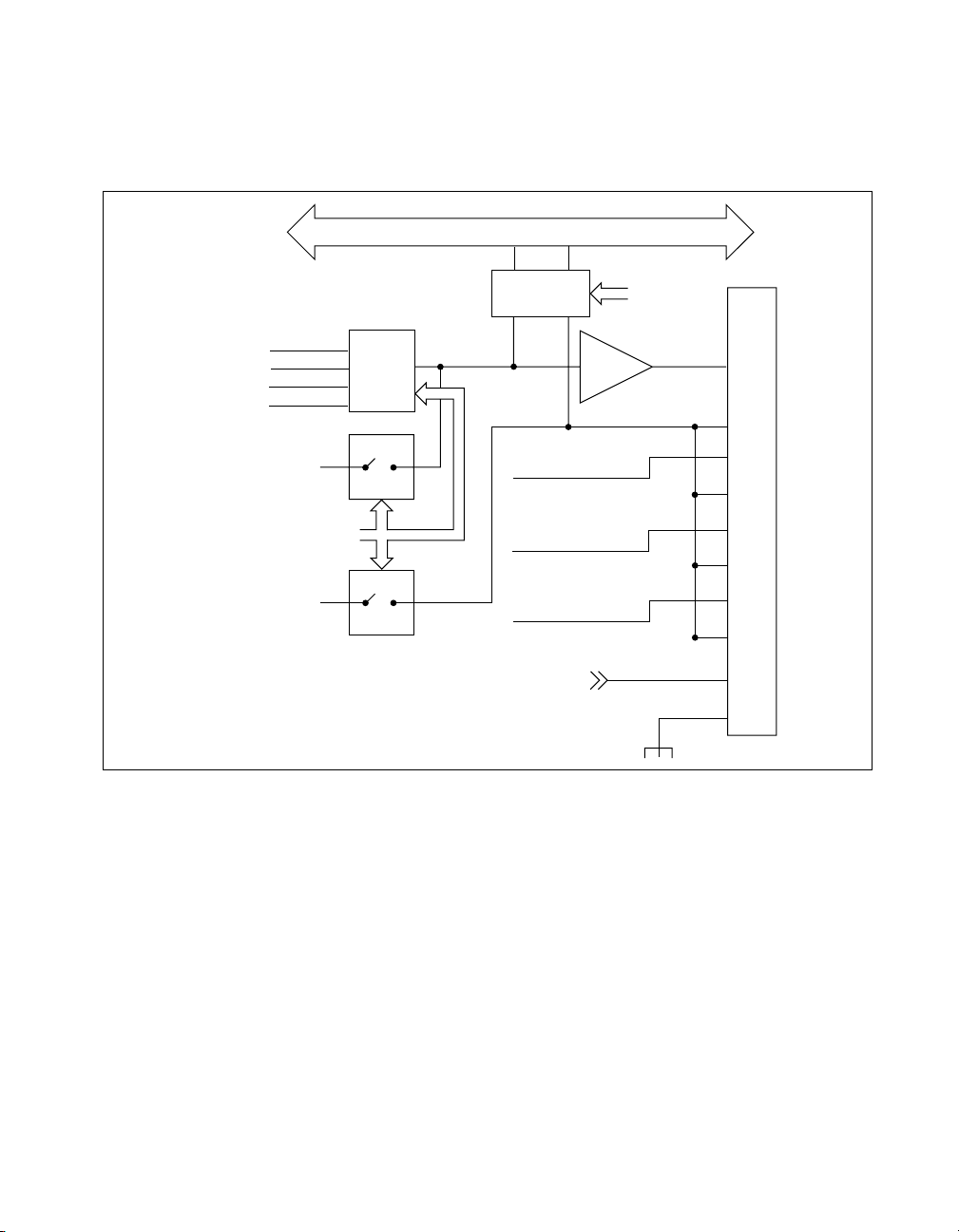
Analog Output Circuitry
Figure 3-6 shows the SCXI-1121 analog output circuitry.
Chapter 3 Theory of Operation
SCXIbus
Channel 0
Channel 1
Channel 2
Channel 3
MTEMP
Output Stage and
Hardware Scan Control
Analog
Reference
Output
Mux
AB0
Switch
Channel 1
From
Channel 2
From
Channel 3
DTEMP
Figure 3-6.
Output
Stage
Control
Buffer
MCH1+From
MCH2+
MCH3+
MCH0+
MCH0–
MCH1–
MCH2–
MCH3–
MCH4+
MCH4–
Analog Output Circuitry
Rear Signal Connector
The SCXI-1121 output circuitry consists of a buffered-output multiplexer
and channel-select hardware. The channel-select hardware consists of a
two-bit counter, MUXCOUNTER. This counter is needed when the board
is operating in the Multiplexed-Output Mode. The counter output is sent to
the multiplexer address pins to determine which of the four channels is to
be connected to MCH0. In the Single-Channel Read mode, the
MUXCOUNTER is loaded with the desired channel number. In the
Scanning mode, the counter is loaded with the first channel to be read.
During the scan, the counter is clocked by SCANCLK from the data
acquisition board, or TRIG0 from the SCXIbus, depending on the state of
the CLKSELECT bit in the Configuration Register. During scanning
operations, the MUXCOUNTER is reloaded with the channel value stored
© National Instruments Corporation 3-15 SCXI-1121 User Manual
Page 78

Chapter 3 Theory of Operation
in the Configuration Register when SCANCON is high (inacti ve) and will
count upwards on each rising clock edge when SCANCON is low (acti ve).
In the Parallel-Output Mode, the MUXCOUNTER is disabled and its
output indicates binary 00 hence, amplifier channel 0 is selected at the
output multiplexer and is connected to MCH0. The three other channels are
hardwired to MCH1 through MCH3 on the rear signal connector.
The output multiplexer multiplexes all four amplifier outputs and the
temperature sensor reading provided on the MTEMP line. To read the
temperature sensor when it is multiplexed with the other input channels, set
the RTEMP bit of the Configuration Register high. This measurement is
only software controlled. For hardware control of the temperature sensor
reading, connect the temperature sensor to MCH4+. Notice that MCH4–,
the DTS reference, is hardwired to the chassis ground. The multiplexer
output connects to the MCH0± and is connected to the data acquisition
board analog channel input. In the case of the MIO data acquisition boards,
MCH0± on the rear signal connector corresponds to ACH0 and ACH8.
Furthermore, you can bus the multiplexed output of the SCXI-1121 via
switches to AB0± on the SCXIbus and on to other modules. When you use
multiple modules, you can bus the output of the module via AB0 to the
module that is connected to the data acquisition board. In this case, the AB0
switches of all the modules are closed, whereas the output multiplexer of
all the modules but the one being read are disabled. Refer to Chapters 2
and 5 for further details on how to configure and program multiple
modules.
In addition to the Multiplexed-Output mode described in the previous
paragraph, you can operate the SCXI-1121 in Parallel-Output mode. In this
mode, you need no software—other than software used with your data
acquisition board—to control the scanning of the four channels or to
perform a single read. To access the temperature sensor in this mode,
configure the temperature sensor in the DTS mode. At power up or at reset,
amplifier channel 0 is selected on the output multiplexer, and hence
connects to MCH0. The other four channels (three amplifier channels and
one temperature channel) are hardwired to the rear signal connector . Notice
that even when you select the Multiplexed-Output mode, the SCXI-1121
drives the rear signal connector pins 5 through 12. The SCXI-1121 outputs
on the rear signal connector are short-circuit protected.
Refer to the following Scanning Modes section for further details on how
to scan the SCXI-1121 channels.
SCXI-1121 User Manual 3-16 www.natinst.com
Page 79

Scanning Modes
There are four basic types of scanning modes possible with the
SCXI-1121—single-module parallel scanning, single-module multiplexed
scanning, multiple-module multiplexed scanning, and multiple-chassis
scanning (possible only with the SCXI-1001 chassis). For additional
information, consult Chapter 2, Configuration and Installation, Chapter 5,
Programming, your data acquisition board manual, and your SCXI chassis
user manual. If you need further information, contact National Instruments.
Single-Module Parallel Scanning
Single-Module parallel scanning is the simplest scanning mode. Directly
cable the SCXI-1121 to the data acquisition board as shown in Figure 3-7.
In this configuration, each analog signal has its own channel. Timing
signals are not necessary for this type of scanning because the module
provides all channels to the data acquisition board at all times. You can
implement single-module parallel scanning with any data acquisition board
that is appropriately cabled to the SCXI-1121.
Chapter 3 Theory of Operation
Data Acquisition BoardSCXI-1121
Cable Assembly
Four Isolated
Floating
Single-Ended
Inputs
CH0
CH1
CH2
CH3
MCH0
MCH1
MCH2
MCH3
Figure 3-7.
Analog Input 0
Analog Input 1
Analog Input 2
Analog Input 3
Single-Module Parallel Scanning
Multiplexed Scanning
Only the MIO-16 data acquisition boards support multiplexed scanning on
the SCXI-1121. During multiplexed scanning, a module sends the
SCANCLK signal to Slot 0 over the TRIG0 backplane line, and Slot 0
sends unique SCANCON signals to each module. Each module uses its
signal to reload MUXCOUNTER and to determine when the SCXI-1121
output is enabled. Slot 0 contains a module list first-in-first-out (FIFO)
memory chip, similar to the Channel/Gain FIFO on an MIO-16 board,
except that instead of having a channel number and gain setting for each
entry, the Slot 0 FIFO contains a slot number and a sample count for each
© National Instruments Corporation 3-17 SCXI-1121 User Manual
Page 80

Chapter 3 Theory of Operation
SCXI-1000 or SCXI-1001 Chassis
entry. The list in Slot 0 will determine which module is being accessed and
for how many samples. It is important that you make sure that the lists on
the data acquisition board and Slot 0 are compatible so that the samples are
acquired as intended. See your SCXI chassis manual for more information.
Single-Module Multiplexed Scanning
Single-Module Multiplexed Scanning (Direct)
This is the simplest multiplexed scanning mode. Directly cable the
SCXI-1121 to the data acquisition board as shown in Figure 3-8. The
module sends SCANCLK onto TRIG0, and Slot 0 sends SCANCON back
to the module. SCANCON will be low at all times during the scan except
during changes from one Slot 0 scan list entry to the next, when
SCANCON pulses high to make the MUXCOUNTER reload its starting
channel. Notice that although you are using only a single module, you can
put many entries with different counts in the Slot 0 FIFO, so that some
channels are read more often than others. You cannot change the start
channel in the module Configuration Register during a scan.
SLOT 0
SCANCON X
TRIG0
Four Isolated
Floating
Single-Ended
Inputs
SLOT X
SCXI-1121
Figure 3-8.
Data Acquisition Board
Cable
SCANCLK
MCH0
Single-Module Multiplexed Scanning (Direct)
Assembly
Timing Output
Analog Input
Single-Module Multiplexed Scanning (Indirect)
In this mode, the SCXI-1121 is not directly cabled to the data acquisition
board. Instead, you connect another module to the data acquisition board,
and the analog output of the SCXI-1121 is sent over Analog Bus 0, through
the intermediate module, and then to the data acquisition board. The
SCXI-1121 receives its MUXCOUNTER clock from TRIG0, which is sent
by the intermediate module, as illustrated in Figure 3-9. Slot 0 operation is
the same for direct connection scanning.
SCXI-1121 User Manual 3-18 www.natinst.com
Page 81

SCANCON X
SLOT 0
Chapter 3 Theory of Operation
SCXI-1000 or SCXI-1001 Chassis
TRIG0
Data Acquisition Board
Cable
Assembly
Timing Output
Analog Input
SCXI-1121
SLOT X
SCANCLK
MCH0
Other
Module
Analog Bus 0
Figure 3-9. Single-Module Multiplexed Scanning (Indirect)
Multiple-Module Multiplexed Scanning
In this mode, all the modules tie into Analog Bus 0, and SCANCON
enables the output of their amplifiers. The module that is directly cabled to
the data acquisition board sends SCANCLK onto TRIG0 for the other
modules and Slot 0, as illustrated in Figure 3-10. The scan list in Slot 0 is
programmed with the sequence of modules and the number of samples per
entry.
SCXI-1000 or SCXI-1001 Chassis
SCANCON X
Data Acquisition Board
Timing
Output
Analog
Input
Cable Assembly
SCANCON A
SLOT 0
SCANCON B
SLOT A
TRIG0
SCXI Module
SLOT B
SCXI ModuleSCXI Module
Analog Bus 0
SLOT X
SCANCLK
MCH0
Figure 3-10. Multiple-Module Multiplexed Scanning
© National Instruments Corporation 3-19 SCXI-1121 User Manual
Page 82
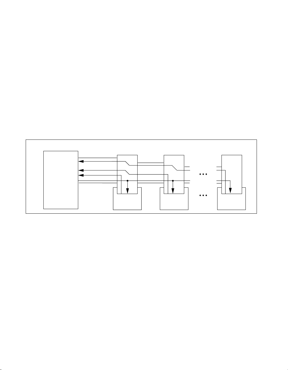
Chapter 3 Theory of Operation
Multiple-Chassis Scanning
In this mode, you attach each SCXI-1001 chassis to a daisy chain of cable
assemblies and multichassis adapter boards, as illustrated in Figure 3-11.
You program each chassis separately, and each chassis occupies a
dedicated channel of the data acquisition board. Within each chassis,
scanning operations act as if the other chassis are not being used, with one
exception. You must program the Slot 0 scan list in each chassis with
dummy entries of Slot 13 to fill the samples when the data acquisition board
will be sampling another chassis or data acquisition board channel. This
will keep the chassis synchronized. Notice that you can only perform
multiple-chassis scanning with the SCXI-1001 chassis and MIO-16 data
acquisition boards. See Chapter 5, Programming, for more information on
multiple-chassis scanning. See Appendix E, SCXI-1121 Cabling, for more
information on the necessary cable accessories for multichassis scanning.
Data Acquisition Board
Input Ch. N
Input Ch. 1
Input Ch. 0
Timing Output
Cable
Assembly
Multichassis
Adapter
Figure 3-11.
Cable
Assembly
Multichassis
Adapter
Cable
Assemblies
Chassis 2Chassis 1
Chassis
Multiple-Chassis Scanning
Multichassis
Adapter
Chassis N
SCXI-1121 User Manual 3-20 www.natinst.com
Page 83

Register Descriptions
This chapter describes in detail the SCXI-1121 Module ID Register, the
Configuration Register, the Slot 0 registers, and multiplexer addressing.
Note
If you plan to use a programming software package such as NI-DAQ, LabWindows,
or LabVIEW with your SCXI-1121 board, you do not need to read this chapter.
Register Description
Register Description Format
The register description chapter discusses each of the SCXI-1121 registers
and the Slot 0 registers. A detailed bit description of each register is given.
The individual register description gives the type, word size, and bit map
of the register, followed by a description of each bit.
The register bit map shows a diagram of the register with the MSB shown
on the left (bit 15 for a 16-bit register, bit 7 for an 8-bit register), and the
LSB shown on the right (bit 0). A rectangle is used to represent each bit.
Each bit is labeled with a name inside its rectangle. An asterisk (*) after the
bit name indicates that the bit is inverted (negative logic). The Module ID
register has a unique format described in the Module ID Register section.
4
In many of the registers, several bits are labeled with an X, indicating don’t
care bits. When you write to a register you may set or clear these bits
without effect.
SCXI-1121 Registers
The SCXI-1121 has two registers. The Module ID Register is a four-byte,
read-only register that contains the Module ID number of the SCXI-1121.
The Configuration Register is a 16-bit, write-only register that controls the
functions and characteristics of the SCXI-1121.
© National Instruments Corporation 4-1 SCXI-1121 User Manual
Page 84

Chapter 4 Register Descriptions
Module ID Register
The Module ID Register contains the 4-byte module ID code for the SCXI-1121. This code
number will be read as the first four b ytes on the MISO line whenev er the module is accessed.
The bytes will appear least significant byte first. Within each byte, data is sent out most
significant bit first. Additional data transfers will result in all zeros being sent on the MISO
line. The Module ID Register is reinitialized to its original value each time the SCXI-1121 is
deselected by the SS* signal on the backplane.
Type: Read-only
Word Size: 4-byte
Bit Map:
Byte 0
76543210
00000010
Byte 1
76543210
00000000
Byte 2
76543210
00000000
Byte 3
76543210
00000000
SCXI-1121 User Manual 4-2 www.natinst.com
Page 85

Chapter 4 Register Descriptions
Configuration Register
The Configuration Register contains 16 bits that control the functions of the SCXI-1121.
When SS* is asserted (low) and D*/A indicates data (low), the register will shift in the data
present on the MOSI line, bit 15 first, and then latch it when the SCXI-1121 is deselected by
the SS* signal on the backplane. The Configuration Register initializes to all zeros when the
SCXI chassis is reset or first turned on.
Type: Write-only
Word Size: 16-bit
Bit Map:
15 14 13 12 11 10 9 8
CLKOUTEN CLKSELECT SCAL X X X CHAN1 CHAN0
76 5 4 3 2 1 0
X X RTEMP RSVD SCANCLKEN SCANCONEN AB0EN FOUTEN*
Bit Name Description
15 CLKOUTEN Scanclock Output Enable—This bit determines whether
the SCANCLK signal from the rear signal connector is
sent out, in inverted form, to the TRIG0 backplane signal.
If CLKOUTEN is set to 1, SCANCLK* is transmitted on
TRIG0. If CLKOUTEN is cleared to 0, SCANCLK* is not
transmitted on TRIG0.
14 CLKSELECT Scanclock Select—This bit determines whether the
SCXI-1121 uses SCANCLK or the inverted form of
TRIG0 to clock the MUXCOUNTER for the purpose of
scanning through the analog channels. If CLKSELECT is
cleared to 0, SCANCLK is used to clock MUXCOUNTER.
If CLKSELECT is set to 1, TRIG0* is used as the source
to clock MUXCOUNTER.
13 SCAL Shunt Calibrate—This bit determines whether the shunt
calibration switches on the SCXI-1321 are closed or open.
If SCAL is cleared to 0, the switches are open. If SCAL is
set to 1, the shunt calibration switches on the SCXI-1321
are closed and an R
is placed in parallel with the
SCAL
bridge between EX+ and CH+ on all four channels.
12-10, 7-6 X Don’t care bits.
© National Instruments Corporation 4-3 SCXI-1121 User Manual
Page 86

Chapter 4 Register Descriptions
9-8 CHAN<1..0> Channel Select—These bits determine the channel number
5 RTEMP Read Temperature—This bit determines whether the
4 RSVD Reserved—This bit should always be written to zero.
3 SCANCLKEN Scan Clock Enable—This bit determines whether
(zero to three) that is loaded into the MUXCOUNTER to
determine the analog channel to be read during a single
read, or the starting channel on the module for a scanned
data acquisition. CHAN1 is the MSB.
selected channel output or the MTEMP signal is driven
onto the MCH0± pins of the rear signal connector. If
RTEMP is cleared to zero, the selected channel output is
used as the module output. If RTEMP is set to one, the
MTEMP signal is used as the module output. The module
output will only be driven when FOUTEN* is cleared to 0,
or SCANCON is active (low) while SCANCONEN* is
cleared.
MUXCOUNTER will increment on each clock signal
(the clock source is determined by CLKSELECT), or keep
its loaded value. If SCANCLKEN is set to one,
MUXCOUNTER will be clocked during scans. If
SCANCLKEN is cleared to zero, MUXCOUNTER will
not be clocked.
2 SCANCONEN Scan Control Enable—This bit, whe n high, enables the
SCANCON signal.
1 AB0EN Analog Bus 0 Enable—This bit determines whether
Analog Bus 0 on the SCXIbus drives MCH0 on the rear
signal connector. If AB0EN is cleared to zero, Analog
Bus 0 does not drive MCH0. If AB0EN is set to one,
Analog Bus 0 + drives MCH0+ through a buffer and a
Analog Bus 0 – is connected to MCH0–.
SCXI-1121 User Manual 4-4 www.natinst.com
Page 87

0 FOUTEN* Forced Output Enable—This bit determines whether the
Slot 0 Register Descriptions
Slot 0 has three registers. The Slot-Select Register is a 16-bit, write-only
register that determines with which slot the data acquisition board will
speak when SLOT0SEL* is released high. In the case of the SCXI-1001
chassis, the Slot-Select Register also determines in which chassis the
desired slot is. The FIFO Register is a 16-bit, write-only register used for
storing the Slot 0 scan list that determines the chassis scan sequence. The
Hardscan Control Register (HSCR) is an 8-bit, write-only register used for
setting up the timing circuitry in Slot 0. The Slot-Select Register is written
to by using the SLOT0SEL* line. The HSCR and the FIFO Register are
written to as if they were registers located on modules in Slots 13 and 14.
It is recommended that you maintain software copies of the Slot-Select
Register, HSCRs, and all the Slot 0 scan lists that correspond to the writes
to FIFO Registers.
Chapter 4 Register Descriptions
module will drive the MCH0± pins on the rear signal
connector with either the selected channel output or the
MTEMP signal, depending on the state of RTEMP. If
FOUTEN* is cleared to zero, the MCH0± pins will be
driven through a buffer by the selected channel output or
the MTEMP line. If FOUTEN* is set to one, the MCH0±
pins will not be driven by the selected channel output or
MTEMP, unless SCANCON is active (low) and the
SCANCONEN bit is cleared. If the selected channel
output or MTEMP is driving the output buffer, it will d rive
Analog Bus 0 if AB0EN is set. If nothing is driving the
output buffer, the SCXI-1121 output will saturate.
If you are using multiple chassis, it is important to understand the
architectural differences of the Slot-Select Register as compared to the
HSCR and the FIFO Register. Although each chassis has its own physical
Slot-Select Register, all are written to at the same time. The jumper settings
in Slot 0 of a chassis determine with which chassis number Slot 0 is
identified. From the software perspective, only one Slot-Select Register
exists in a system composed of multiple chassis. The HSCR and FIFO
Register, on the other hand, are unique to each chassis and you must
program them separately.
© National Instruments Corporation 4-5 SCXI-1121 User Manual
Page 88

Chapter 4 Register Descriptions
Slot-Select Register
The Slot-Select Register contains 16 bits that determine which module in which chassis will
be enabled for communication when the SLOT0SEL* line is set to one. An SCXI-1000
chassis will select the appropriate module in its chassis, regardless of the chassis number
written. The Slot-Select Register will shift in the data present on the MOSI line, bit 16 first,
when SLOT0SEL* is cleared to zero.
Type: Write-only
Word Size: 16-b it
Bit Map:
15 14 13 12 11 10 9 8
XXXXXXXCHS4
76543210
CHS3 CHS2 CHS1 CHS0 SL3 SL2 SL1 SL0
Bit Name Description
15-9 X Don’t care bits.
8-4 CHS<4..0> Chassis Bit 4 through 0—These bits determine which
chassis is selected. On the SCXI-1000 chassis, these bits
are don’t cares.
3-0 SL<3..0> Slot Bit 3 through 0—These bits determine which slot in
the selected chassis is selected.
SCXI-1121 User Manual 4-6 www.natinst.com
Page 89

Chapter 4 Register Descriptions
Hardscan Control Register (HSCR)
The HSCR contains eight bits that control the setup and operation of the hardscan timing
circuitry of Slot 0. To write to the HSCR, follow the procedure given in the Register Writes
section of Chapter 5, Programming, using 13 as the slot number, and writing eight bits to the
HSCR. The register will shift in the data present on the MOSI line, bit seven first, when
Slot 13 is selected by the Slot-Select Register.
Type: Write-only
Word Size: 8-bit
Bit Map:
765432 1 0
RSVD FRT RD ONCE HSRS* LOAD* SCANCONEN CLKEN
Bit Name Description
7 RSVD Reserved.
6 FRT Forced Retransmit—This bit, when clear, causes the scan
list in the FIFO to be reinitialized to the first entry, thus
allowing the scan list to be reprogrammed in two steps
instead of having to rewrite the entire list. When this bit is
set, it has no effect.
5 RD Read—This bit, when clear, prevents the FIFO from being
read. When set, the FIFO is being read except at the end of
a scan list entry during scanning, when reading is briefly
disabled to advance to the next scan list entry.
4 ONCE Once—When set, this bit will cause the Hardscan circuitry
to shut down at the end of the scan list circuitry during a
data acquisition. When clear, the circuitry will wrap
around and continue with the first scan list entry after the
entry is finished.
3 HSRS* Hardscan Reset—When clear, this bit causes all the
hardware scanning circuitry, including the FIFO, to be
reset to the power up state. When set, this bit has no effect.
2 LOAD* Load—T his bit, when clear, forces a loading of the Slot 0
sample counter with the output of the FIFO. When set, this
bit has no effect.
© National Instruments Corporation 4-7 SCXI-1121 User Manual
Page 90

Chapter 4 Register Descriptions
1 SCANCONEN Scan Control Enable—When set, this bit enable s the
0 CLKEN Clock Enable—When set, this bit enables TRIG0 as a
SCANCON lines. When clear, all SCANCON lines are
disabled (high).
clock for the hardscan circuitry. When clear, TRIG0 is
disabled.
SCXI-1121 User Manual 4-8 www.natinst.com
Page 91

Chapter 4 Register Descriptions
FIFO Register
The FIFO Register is used to add entries to the Slot 0 FIFO. The FIFO contains the Slot 0 scan
list. Each entry contains a slot number to be accessed, and a count number to determine the
number of samples to be taken from that slot. To write to the FIFO Register, follow the
procedure given in the Register Writes section of Chapter 5, Programming, using 14 as the
slot number, and writing 16 bits to the FIFO Register . The register will shift in the data present
on the MOSI line, bit 15 first, when Slot 14 is selected by the Slot-Select Register. The Slot 0
scan list is created by consecutive writes to the FIFO Register. Each write creates a new entry
at the end of the scan list. The maximum number of entries is 256. To clear the FIFO of all
entries, clear the HSRS* bit in the HSCR.
Type: Write-only
Word Size: 16-b it
Bit Map:
15 14 13 12 11 10 9 8
X X X X X MOD3 MOD2 MOD1
76543210
MOD0 CNT6 CNT5 CNT4 CNT3 CNT2 CNT1 CNT0
Bit Name Description
15-11 X Don’t care bits—Unused.
10-7 MOD<3..0>Module Number—The value of these bits plus
on determines the number of the slot to be accessed fo r this
scan entry. For example, to access Slot 6, MOD<3..0>
would be 0101.
6-0 CNT<6..0> Count—The value of th ese bits plus one determines ho w
many samples will be taken before the next scan list entry
becomes active. A value of zero corresponds to one sample
and a value of 127 corresponds to 128 samples.
© National Instruments Corporation 4-9 SCXI-1121 User Manual
Page 92

Programming
This chapter contains a functional programming description of the
SCXI-1121 and Slot 0.
Note
If you plan to use a programming software package such as NI-DAQ, LabWindows,
or LabVIEW with your SCXI-1121 board, you do not need to read this chapter.
Programming Considerations
Programming the SCXI-1121 involves writing to the Configuration
Register. Programming Slot 0 involves writing to the HSCR and FIFO
Register. Programming the data acquisition boards involves writes to their
registers. See your data acquisition board user manual for more
information. The programming instructions list the sequence of steps to
take. The instructions are language independent that is, they instruct you to
write a value to a given register without presenting the actual code.
Notation
For the bit patterns to be written, the following symbols are used:
5
0 Binary zero
1 Binary one
X Don't care, either zero or one may be written
C One of two bits used to specify the channel to be loaded into the
MUXCOUNTER. This value will either be the channel to be read for
single reads, or a starting channel for scanned measurements.
The 16-bit patterns are presented MSB first, left to right.
© National Instruments Corporation 5-1 SCXI-1121 User Manual
Page 93

Chapter 5 Programming
Register Writes
This section describes how to write to the Configuration Register, HSCR,
and FIFO Register including the procedure for writing to the Slot-Select
Register to select the appropriate slot. For timing specifics, refer to the
Timing Requirements and Communication Protocol section in Chapter2,
Configuration and Installation. The rear signal connector pin equivalences
to the different National Instruments data acquisition boards are given in
Table5-1. See also AppendixE, SCXI-1121 Cabling. The Configuration
Register, the FIFO Register, and the HSCR are write-only registers.
The different bits in these registers often control independent pieces of
circuitry. There are times when you may want to set or clear a specific bit
or bits without affecting the remaining bits. However, a write to one of these
registers will affect all bits simultaneously. You cannot read the registers to
determine which bits have been set or cleared in the past therefore, you
should maintain a software copy of these registers. You can then read the
software copy to determine the status of the register. To change the state of
a single bit without disturbing the remaining bits, set or clear the bit in the
software copy and write the software copy to the register.
Table 5-1.
SCXI-1121
SCXIbus
Line
MOSI SERDATIN ADIO0 PB4 DOUT4
D*/A DAQD*/A ADIO1 PB5 DOUT5
INTR* SLOT0SEL* ADIO2 PB6 DOUT6
SPICLK SERCLK EXTSTROBE* PB7 DOUT7
MISO SERDATOUT BDIO0 PC1 DIN6
Rear Signal
Connector
SCXI-1121 Rear Signal Connector Pin Equivalences
MIO-16 Lab Board PC-LPM-16
Register Selection and Write Procedure
1. Select the slot of the module to be written to (or Slot 13 or 14). Initial
conditions:
SERDATIN = X
DAQD*/A = X
SLOT0SEL* = 1
SERCLK = 1
2. Clear SLOT0SEL* to 0. This will deassert all SS* lines to all modules
in all chassis.
SCXI-1121 User Manual 5-2 www.natinst.com
Page 94

Chapter 5 Programming
3. For each bit, starting with the MSB first (bit 15):
a. SERDATIN = bit to be sent. These bits are the data that is being
written to the Slot-Select Register.
b. Clear SERCLK to 0.
c. Set SERCLK to 1. This rising edge clocks the data. (If you are
using an MIO-16 board, writing to the EXTSTROBE* register
will pulse EXTSTROBE* low and then high, accomplishing
steps 3b and 3c.)
4. Set SLOT0SEL* to 1. This will assert the SS* line of the module
whose slot number was written to Slot 0. If you are using multiple
chassis, the appropriate slot in the chassis whose address corresponds
to the written chassis number will be selected automatically. When no
communications are taking place between the data acquisition board
and any modules, write zero to the Slot-Select Register to ensure that
no accidental writes occur.
5. If you are writing to a Configuration Register, clear DAQD*/A to 0
(this indicates data will be written to the Configuration Register). If
you are writing to the HSCR or FIFO Register, leave DAQD*/A high.
6. For each bit to be written to the Configuration Register:
a. Establish the desired SERDATIN level corresponding to this bit.
b. Clear SERCLK to 0.
c. Set SERCLK to 1 (clock the data). (If you are using an MIO-16
board, writing to the EXTSTROBE* register will pulse
EXTSTROBE* low and then high, accomplishing steps 6b
and 6c.)
7. Pull SLOT0SEL* low to deassert the SS* line, latch the data into the
Configuration Register and establish conditions for writing a new slot
select number to the Slot 0 Slot-Select Register.
8. If you are not selecting another slot, write zero to the Slot 0 Slot-Select
Register. If you are selecting another slot, start at step 3.
For a timing illustration of a Configuration Register write, see Figure 2-18,
Configuration Register Write Timing Diagram, which shows the proper
write to configure an SCXI-1121 that is directly cabled to an MIO-16 for
multiple-module multiplexed scanning with a start channel of 3.
Initialization
The SCXI-1121 powers up with its Configuration register cleared to all
zeros. You can force this state by an active low signal on the RESET* pin
of the backplane connector. In the reset state, CH0 through CH3 are routed
© National Instruments Corporation 5-3 SCXI-1121 User Manual
Page 95

Chapter 5 Programming
to MCH0 through MCH3 on the rear signal connector. The module is
disconnected from Analog Bus 0 and disabled from scanning.
Single-Channel Measurements
This section describes how to program the SCXI-1121, either alone or in
conjunction with other modules, to make single-channel, or nonscanned,
measurements.
Direct Measurements
Parallel Output
In order to perform a parallel output measurement, you must cable the
SCXI-1121 rear signal connector to a data acquisition board with each
output connected to a different data acquisition board channel. See
Chapter 2, Configuration and Installation, for more information. For
information on how to make the voltage measurement with your data
acquisition board, consult your data acquisition board user manual.
Remember to account for the gains of both the SCXI-1121 and the data
acquisition board when calculating the actual voltage present at the input of
the SCXI-1121.
T o measure one of the four differential input channels to the SCXI-1121, or
the DTEMP line if the module has been configured appropriately , perform
the following steps:
1. Write the binary pattern
Configuration Register. Notice that this can be the RESET state.
2. Measure the voltage with the data acquisition board.
000XXX00 XX000000 to the SCXI-1121
Multiplexed Output
In order to perform a direct multiplexed output measurement, you must
cable the SCXI-1121 rear signal connector to a data acquisition board.
See Chapter 2, Configura tion and Installation, for more information. For
information on how to make the voltage measurement with your data
acquisition board, consult your data acquisition board user manual.
Remember to account for the gains of both the SCXI-1121 and the data
acquisition board when calculating the actual voltage present at the input
of the SCXI-1121.
SCXI-1121 User Manual 5-4 www.natinst.com
Page 96

Chapter 5 Programming
To measure one of the four differential input channels to the SCXI-1121,
perform the following steps:
1. Write the binary pattern
000XXXCC XX000000 to the SCXI-1121
Configuration Register.
2. Measure the voltage with the data acquisition board.
To shunt calibrate one of the four differential input channels, perform the
following steps:
1. Write the binary pattern
001XXXCC XX00000 to the SCXI-1121
Configuration Register. Insert a delay of at least 1 sec if you have set
the 4 Hz filter , or at least 1 msec if you ha v e set the 10 kHz f ilter. This
delay permits the SCXI-1121 amplifier to settle.
2. Measure the voltage with the data acquisition board.
To measure the voltage on the MTEMP line, perform the following steps:
1. Write the binary pattern
000XXXXX XX100000 to the SCXI-1121
Configuration Register.
2. Measure the voltage with the data acquisition board.
Indirect Measurements
Indirect measurements involve one module sending a signal to Analog
Bus 0, where it is picked up by another module and transmitted to the data
acquisition board.
Measurements from Other Modules
To perform measurements from other modules, you must cable the
SCXI-1121 rear signal connector to a data acquisition board. See
Chapter 2, Configuration and Installation, for more information. To make
a measurement from another module, perform the following steps:
1. Perform any necessary programming to ensure that no modules are
driving Analog Bus 0. For an SCXI-1121, clearing AB0EN in the
Configuration Register will ensure that its output is not driving AB0.
2. Write the binary pattern
Configuration Register . This step disables the SCXI-1121 from driving
Analog Bus 0 and allows Analog Bus 0 to drive MCH0 through the
output buffer.
3. Program the other module to drive Analog Bus 0 with the signal to be
measured.
4. Measure the voltage with the data acquisition board.
© National Instruments Corporation 5-5 SCXI-1121 User Manual
000XXXXX XX100011 to the SCXI-1121
Page 97

Chapter 5 Programming
Measurements from the SCXI-1121 via Another Module
To perform measurements via another module, you must cable the other
module rear signal connector to a data acquisition board. The other module
must also be able to transfer Analog Bus 0 to the data acquisition board. See
Chapter 2, Configuration and Installation, for more information.
To measure one of the four differential input channels to the SCXI-1121,
perform the following steps:
1. Perform any necessary programming to ensure that no modules are
driving Analog Bus 0. For an SCXI-1121, clearing AB0EN in the
Configuration Register will ensure that its output is not driving AB0.
2. Program the other module not to drive Analog Bus 0, but to send
Analog Bus 0 to the data acquisition board.
3. Write the binary pattern
Configuration Register.
4. Measure the voltage with the data acquisition board.
T o perform a shunt calibration on one of the four differential input channels
of the SCXI-1121, perform the following steps:
1. Perform any necessary programming to ensure that no modules are
driving Analog Bus 0. For an SCXI-1121, clearing AB0EN in the
Configuration Register will ensure that its output is not driving AB0.
2. Program the other module not to drive Analog Bus 0, but to send
Analog Bus 0 to the data acquisition board.
3. Write the binary pattern
Configuration Register.
4. Insert a delay equal to 1 sec if you have set the 4 Hz filter , or 1 msec if
you have set the 10 kHz filter. This delay permits the SCXI-1121
amplifier to settle.
5. Measure the voltage with the data acquisition board.
000XXXCC XX000010 to the SCXI-1121
001XXXCC XX000010 to the SCXI-1121
To measure the voltage on the MTEMP line, perform the following steps:
1. Perform any necessary programming to ensure that no modules are
driving Analog Bus 0. For an SCXI-1121, clearing AB0EN in the
Configuration Register will ensure that its output is not driving AB0.
2. Program the other module not to drive Analog Bus 0, but to send
Analog Bus 0 to the data acquisition board.
3. Write the binary pattern
000XXXXX XX100010 to the SCXI-1121
Configuration Register.
4. Measure the voltage with the data acquisition board.
SCXI-1121 User Manual 5-6 www.natinst.com
Page 98

Scanning Measurements
Programming for scanned data acquisition involves programming your
data acquisition board, modules, and Slot 0. In general, the steps to be taken
are as follows:
1. Perform all data acquisition board programming to the point of
enabling the data acquisition.
2. Perform all module programming.
3. Program the Slot 0 hardscan circuitry.
4. Enable the data acquisition, trigger it either through software or
hardware, and service the data acquisition.
The MIO and Lab-PC+ boards can do all types of scanning. Lab-NB,
Lab-PC, Lab-PC+, Lab-LC, and PC-LPM-16 boards support only
single-module parallel scanning, and do not support any of the multiplexed
scanning modes. Notice that single-module parallel scanning is typically
done without any module or Slot 0 programming only programming the
data acquisition board is necessary.
1. Data Acquisition Board Setup Programming
The programming steps for your data acquisition board are given in your
data acquisition board user manual. You should follow the instructions in
the following sections:
• AT-MIO-16 User Manual
– Multiple A/D Conversions with Continuous Channel Scanning
– Multiple A/D Conversions with Interval Channel Scanning
• AT-MIO-16D User Manual
– Multiple A/D Conversions with Continuous Channel Scanning
– Multiple A/D Conversions with Interval Channel Scanning
• AT-MIO-16F-5 User Manual
– Posttrigger Data Acquisition with Continuous Channel Scanning
– Posttrigger Data Acquisition with Interval Channel Scanning
Chapter 5 Programming
(Round Robin)
(Pseudosimultaneous)
(Round Robin)
(Pseudosimultaneous)
© National Instruments Corporation 5-7 SCXI-1121 User Manual
Page 99

Chapter 5 Programming
• AT-MIO-16X User Manual
– Continuous Channel Scanning Data Acquisition
– Interval Channel Scanning Data Acquisition
• AT-MIO-64F-5 User Manual
– Continuous Channel Scanning Data Acquisition
– Interval Channel Scanning Data Acquisition
• Lab-LC User Manual
– Programming Multiple A/D Conversions with Channel Scanning
• Lab-NB User Manual
– Programming Multiple A/D Conversions with Channel Scanning
• Lab-PC User Manual
– Programming Multiple A/D Conversions with Channel Scanning
• Lab-PC+ User Manual
– Programming Multiple A/D Conversions with Channel Scanning
– Programming Multiple A/D Conversions with Interval Scanning
– Programming Multiple A/D Conversions in Single-Channel
Interval Acquisition Mode
• MC-MIO-16 User Manual
– Multiple A/D Conversions with Continuous Channel Scanning
(Round Robin)
– Multiple A/D Conversions with Interval Channel Scanning
(Pseudosimultaneous)
• NB-MIO-16 User Manual
– Programming Multiple A/D Conversions with Channel Scanning
• NB-MIO-16X User Manual
– Multiple A/D Conversions with Continuous Channel Scanning
(Round Robin)
– Multiple A/D Conversions with Interval Channel Scanning
(Pseudosimultaneous)
• PC-LPM-16 User Manual
– Programming Multiple A/D Conversions with Channel Scanning
SCXI-1121 User Manual 5-8 www.natinst.com
Page 100

Chapter 5 Programming
Follow the instructions in these sections through the part labeled as follows:
• Clear the A/D Circuitry and Reset the Mux Counter in the MIO board
user manual (except for the AT -MIO-16X and the AT -MIO-64F-5). Do
not continue to the part called Enable the Scanning Data Acquisition
Operation. You will do this after you program the modules and Slot 0.
• Program the Sample Counter (if you are doing continuous channel
scanning) or Program the Scan-Interval Counter (if you are doing
interval channel scanning) in the A T-MIO-16X or A T-MIO-64F-5 user
manual. Do not continue to the part labeled Enable a Scanning Data
Acquisition Operation or Enable an Interval Scanning Data
Acquisition Operation. Y ou will do this after you program the modules
and Slot 0.
Note For multiplexed scanning with an MIO board, it is important that you follow the
instructions in the channel-scanning sections, not the single-channel sections. Although
you may be using only one MIO board channel, the channel scanning programming will
ensure that the MIO board outputs SCANCLK, which is needed by the SCXI-1120 and
Slot 0.
• Clear the A/D Circuitry in the Lab-LC User Manual. Do not continue
to the part called Program the Sample-Interval Counter. You will do
this after you program the modules and Slot 0.
• Clear the A/D Circuitry in the Lab-PC User Manual, the Lab-PC+
User Manual, and the PC-LPM-16 User Manual. Do not continue to
the part called Start and Service the Data Acquisition Operation. You
will do this after you program the modules and Slot 0.
• Clear the A/D Circuitry in the Lab-NB User Manual. Do not continue
to the part called Program the Sample-Interval Counter (Counter A0).
You will do this after you program the modules and Slot 0.
Counter 1 and SCANDIV
All MIO boards can operate their data acquisition board scan lists in two
ways—they can acquire one sample per data acquisition board scan list
entry or they can acquire N samples per data acquisition board scan list
entry, where N is a number from 2 to 65,535 that is programmed in
Counter 1. This second method of operation is especially useful when the
data acquisition board scan list length is limited to 16 entries, as it is on all
MIO boards except the AT-MIO-16F-5, which can have up to 512 entries.
Because you can multiplex many SCXI-1121s in one chassis to one MIO
board channel, often the simplest way to program the MIO board is to use
only one data acquisition board scan list entry, and make N the total number
of samples to be taken on all modules in one scan. Check your MIO board
user manual for limitations in the data acquisition board scan list format.
© National Instruments Corporation 5-9 SCXI-1121 User Manual
 Loading...