

Page 1

DAQ
SCB-68 68-Pin Shielded Connector Block User Manual
SCB-68 Shielded Connector Block User Manual
December 2002 Edition
Part Number 320745B-01
Page 2

Support
Worldwide Technical Support and Product Information
ni.com
National Instruments Corporate Headquarters
11500 North Mopac Expressway Austin, Texas 78759-3504 USA Tel: 512 683 0100
Worldwide Offices
Australia 03 9879 5166, Austria 0662 45 79 90 0, Belgium 02 757 00 20, Brazil 55 11 3262 3599,
Canada (Calgary) 403 274 9391, Canada (Montreal) 514 288 5722, Canada (Ottawa) 613 233 5949,
Canada (Québec) 514 694 8521, Canada (Toronto) 905 785 0085, China 86 21 6555 7838,
Czech Republic 02 2423 5774, Denmark 45 76 26 00, Finland 09 725 725 11, France 01 48 14 24 24,
Germany 089 741 31 30, Greece 01 42 96 427, Hong Kong 2645 3186, India 91 80 4190000,
Israel 03 6393737, Italy 02 413091, Japan 03 5472 2970, Korea 02 3451 3400, Malaysia 603 9596711,
Mexico 001 800 010 0793, Netherlands 0348 433466, New Zealand 09 914 0488, Norway 32 27 73 00,
Poland 22 3390 150, Portugal 210 311 210, Russia 095 238 7139, Singapore 65 6 226 5886,
Slovenia 3 425 4200, South Africa 11 805 8197, Spain 91 640 0085, Sweden 08 587 895 00,
Switzerland 056 200 51 51, Taiwan 02 2528 7227, United Kingdom 01635 523545
For further support information, refer to the Technical Support and Professional Services appendix. To comment
on the documentation, send email to techpubs@ni.com.
© 1994–2002 National Instruments Corporation. All rights reserved.
Page 3

Important Information
Warranty
The SCB-68 is warranted against defects in materials and workmanship for a period of one year from the date of shipment, as evidenced by
receipts or other documentation. National Instruments will, at its option, repair or replace equipment that proves to be defective during the
warranty period. This warranty includes parts and labor.
The media on which you receive National Instruments software are warranted not to fail to execute programming instructions, due to defects
in materials and workmanship, for a period of 90 days from date of shipment, as evidenced by receipts or other documentation. National
Instruments will, at its option, repair or replace software media that do not execute programming instructions if National Instruments receives
notice of such defects during the warranty period. National Instruments does not warrant that the operation of the software shall be
uninterrupted or error free.
A Return Material Authorization (RMA) number must be obtained from the factory and clearly marked on the outside of the package before
any equipment will be accepted for warranty work. National Instruments will pay the shipping costs of returning to the owner parts which are
covered by warranty.
National Instruments believes that the information in this document is accurate. The document has been carefully reviewed for technical
accuracy. In the event that technical or typographical errors exist, National Instruments reserves the right to make changes to subsequent
editions of this document without prior notice to holders of this edition. The reader should consult National Instruments if errors are suspected.
In no event shall National Instruments be liable for any damages arising out of or related to this document or the information contained in it.
XCEPT AS SPECIFIED HEREIN, NATIONAL INSTRUMENTS MAKES NO WARRANTIES, EXPRESS OR IMPLIED, AND SPECIFICALLY DISCLAIMS ANY WAR RANTY OF
E
MERCHANTABILITY OR FITNESS FOR A PARTICULAR PURPOSE . CUSTOMER’S RIGHT TO RECOVER DAMAGES CAUSED BY FAULT OR NEGLIGENCE ON THE PART OF
N
ATIONAL INSTRUMENTS SHALL BE LIMITED TO THE AMOUNT THERETOFORE PAID BY THE CUSTOMER. NATIONAL INSTRUMENTS WILL NOT BE LIABLE FOR
DAMAGES RESULTING FROM LOSS OF DATA, PROFITS, USE OF PRODUCTS, OR INCIDENTAL OR CONSEQUENTIAL DAMAGES, EVEN IF ADVISED OF THE PO SSIBILITY
THEREOF. This limitation of the liability of National Instruments will apply regardless of the form of action, whether in contract or tort, including
negligence. Any action against National Instruments must be brought within one year after the cause of action accrues. National Instruments
shall not be liable for any delay in performance due to causes beyond its reasonable control. The warranty provided herein does not cover
damages, defects, malfunctions, or service failures caused by owner’s failure to follow the National Instruments installation, operation, or
maintenance instructions; owner’s modification of the product; owner’s abuse, misuse, or negligent acts; and power failure or surges, fire,
flood, accident, actions of third parties, or other events outside reasonable control.
Copyright
Under the copyright laws, this publication may not be reproduced or transmitted in any form, electronic or mechanical, including photocopying,
recording, storing in an information retrieval system, or translating, in whole or in part, without the prior written consent of National
Instruments Corporation.
Trademarks
DAQCard™, National Instruments™, NI™, and ni.com™ are trademarks of National Instruments Corporation.
Product and company names mentioned herein are trademarks or trade names of their respective companies.
Patents
For patents covering National Instruments products, refer to the appropriate location: Help»Patents in your software, the patents.txt file
on your CD, or
ni.com/patents.
WARNING REGARDING USE OF NATIONAL INSTRUMENTS PRODUCTS
(1) NATIONAL INSTRUMENTS PRODUCTS ARE NOT DESIGNED WITH COMPONENTS AND TESTING FOR A LEVEL OF
RELIABILITY SUITABLE FOR USE IN OR IN CONNECTION WITH SURGICAL IMPLANTS OR AS CRITICAL COMPONENTS IN
ANY LIFE SUPPORT SYSTEMS WHOSE FAILURE TO PERFORM CAN REASONABLY BE EXPECTED TO CAUSE SIGNIFICANT
INJURY TO A HUMAN.
(2) IN ANY APPLICATION, INCLUDING THE ABOVE, RELIABILITY OF OPERATION OF THE SOFTWARE PRODUCTS CAN BE
IMPAIRED BY ADVERSE FACTORS, INCLUDING BUT NOT LIMITED TO FLUCTUATIONS IN ELECTRICAL POWER SUPPLY,
COMPUTER HARDWARE MALFUNCTIONS, COMPUTER OPERATING SYSTEM SOFTWARE FITNESS, FITNESS OF COMPILERS
AND DEVELOPMENT SOFTWARE USED TO DEVELOP AN APPLICATION, INSTALLATION ERRORS, SOFTWARE AND
HARDWARE COMPATIBILITY PROBLEMS, MALFUNCTIONS OR FAILURES OF ELECTRONIC MONITORING OR CONTROL
DEVICES, TRANSIENT FAILURES OF ELECTRONIC SYSTEMS (HARDWARE AND/OR SOFTWARE), UNANTICIPATED USES OR
MISUSES, OR ERRORS ON THE PART OF THE USER OR APPLICATIONS DESIGNER (ADVERSE FACTORS SUCH AS THESE ARE
HEREAFTER COLLECTIVELY TERMED “SYSTEM FAILURES”). ANY APPLICATION WHERE A SYSTEM FAILURE WOULD
CREATE A RISK OF HARM TO PROPERTY OR PERSONS (INCLUDING THE RISK OF BODILY INJURY AND DEATH) SHOULD
NOT BE RELIANT SOLELY UPON ONE FORM OF ELECTRONIC SYSTEM DUE TO THE RISK OF SYSTEM FAILURE. TO AVOID
DAMAGE, INJURY, OR DEATH, THE USER OR APPLICATION DESIGNER MUST TAKE REASONABLY PRUDENT STEPS TO
PROTECT AGAINST SYSTEM FAILURES, INCLUDING BUT NOT LIMITED TO BACK-UP OR SHUT DOWN MECHANISMS.
BECAUSE EACH END-USER SYSTEM IS CUSTOMIZED AND DIFFERS FROM NATIONAL INSTRUMENTS' TESTING
PLATFORMS AND BECAUSE A USER OR APPLICATION DESIGNER MAY USE NATIONAL INSTRUMENTS PRODUCTS IN
COMBINATION WITH OTHER PRODUCTS IN A MANNER NOT EVALUATED OR CONTEMPLATED BY NATIONAL
INSTRUMENTS, THE USER OR APPLICATION DESIGNER IS ULTIMATELY RESPONSIBLE FOR VERIFYING AND VALIDATING
THE SUITABILITY OF NATIONAL INSTRUMENTS PRODUCTS WHENEVER NATIONAL INSTRUMENTS PRODUCTS ARE
INCORPORATED IN A SYSTEM OR APPLICATION, INCLUDING, WITHOUT LIMITATION, THE APPROPRIATE DESIGN,
PROCESS AND SAFETY LEVEL OF SUCH SYSTEM OR APPLICATION.
Page 4

Compliance
FFCC/Canada Radio Frequency Interference Compliance
Determining FCC Class
The Federal Communications Commission (FCC) has rules to protect wireless communications from interference. The FCC
places digital electronics into two classes. These classes are known as Class A (for use in industrial-commercial locations only)
or Class B (for use in residential or commercial locations). Depending on where it is operated, this product could be subject to
restrictions in the FCC rules. (In Canada, the Department of Communications (DOC), of Industry Canada, regulates wireless
interference in much the same way.)
Digital electronics emit weak signals during normal operation that can affect radio, television, or other wireless products. By
examining the product you purchased, you can determine the FCC Class and therefore which of the two FCC/DOC Warnings
apply in the following sections. (Some products may not be labeled at all for FCC; if so, the reader should then assume these are
Class A devices.)
FCC Class A products only display a simple warning statement of one paragraph in length regarding interference and undesired
operation. Most of our products are FCC Class A. The FCC rules have restrictions regarding the locations where FCC Class A
products can be operated.
FCC Class B products display either a FCC ID code, starting with the letters EXN,
or the FCC Class B compliance mark that appears as shown here on the right.
Consult the FCC Web site at
FCC/DOC Warnings
This equipment generates and uses radio frequency energy and, if not installed and used in strict accordance with the instructions
in this manual and the CE Marking Declaration of Conformity*, may cause interference to radio and television reception.
Classification requirements are the same for the Federal Communications Commission (FCC) and the Canadian Department
of Communications (DOC).
Changes or modifications not expressly approved by National Instruments could void the user’s authority to operate the
equipment under the FCC Rules.
http://www.fcc.gov for more information.
Class A
Federal Communications Commission
This equipment has been tested and found to comply with the limits for a Class A digital device, pursuant to part 15 of the FCC
Rules. These limits are designed to provide reasonable protection against harmful interference when the equipment is operated
in a commercial environment. This equipment generates, uses, and can radiate radio frequency energy and, if not installed and
used in accordance with the instruction manual, may cause harmful interference to radio communications. Operation of this
equipment in a residential area is likely to cause harmful interference in which case the user will be required to correct
the interference at his own expense.
Canadian Department of Communications
This Class A digital apparatus meets all requirements of the Canadian Interference-Causing Equipment Regulations.
Cet appareil numérique de la classe A respecte toutes les exigences du Règlement sur le matériel brouilleur du Canada.
Class B
Federal Communications Commission
This equipment has been tested and found to comply with the limits for a Class B digital device, pursuant to part 15 of the
FCC Rules. These limits are designed to provide reasonable protection against harmful interference in a residential installation.
This equipment generates, uses, and can radiate radio frequency energy and, if not installed and used in accordance with the
instructions, may cause harmful interference to radio communications. However, there is no guarantee that interference will not
occur in a particular installation. If this equipment does cause harmful interference to radio or television reception, which can
be determined by turning the equipment off and on, the user is encouraged to try to correct the interference by one or more of
the following measures:
• Reorient or relocate the receiving antenna.
• Increase the separation between the equipment and receiver.
• Connect the equipment into an outlet on a circuit different from that to which the receiver is connected.
• Consult the dealer or an experienced radio/TV technician for help.
Page 5

Canadian Department of Communications
This Class B digital apparatus meets all requirements of the Canadian Interference-Causing Equipment Regulations.
Cet appareil numérique de la classe B respecte toutes les exigences du Règlement sur le matériel brouilleur du Canada.
Compliance to EU Directives
Readers in the European Union (EU) must refer to the Manufacturer’s Declaration of Conformity (DoC) for information*
pertaining to the CE Marking compliance scheme. The Manufacturer includes a DoC for most every hardware product except
for those bought for OEMs, if also available from an original manufacturer that also markets in the EU, or where compliance is
not required as for electrically benign apparatus or cables.
To obtain the DoC for this product, click Declaration of Conformity at
by product family. Select the appropriate product family, followed by your product, and a link to the DoC appears in Adobe
Acrobat format. Click the Acrobat icon to download or read the DoC.
* The CE Marking Declaration of Conformity will contain important supplementary information and instructions for the user
or installer.
ni.com/hardref.nsf/. This Web site lists the DoCs
Page 6

Contents
About This Manual
Conventions ...................................................................................................................xi
NI Documentation..........................................................................................................xii
Chapter 1
Introduction
What You Need to Get Started ...................................................................................... 1-1
Quick Reference Label .................................................................................................. 1-2
Installing Cables ............................................................................................................1-5
Using 68-Pin Cables ........................................................................................1-5
Using 100-Pin Cables ......................................................................................1-6
Configuring the SCB-68 ................................................................................................1-11
Safety Information ......................................................................................................... 1-11
Chapter 2
Parts Locator and Wiring Guide
Switch Configuration.....................................................................................................2-3
Chapter 3
Connecting Signals
Connecting Analog Input Signals .................................................................................. 3-1
Input Modes.....................................................................................................3-1
Nonreferenced or Floating Signal Sources......................................................3-3
Differential Inputs ............................................................................. 3-3
Single-Ended Inputs..........................................................................3-3
Ground-Referenced Signal Sources ................................................................3-4
Differential Inputs ............................................................................. 3-4
Single-Ended Inputs..........................................................................3-4
Differential Connection Considerations (DIFF Input Mode)..........................3-5
Differential Connections for Ground-Referenced Signal Sources.... 3-6
Differential Connections for Nonreferenced
or Floating Signal Sources .............................................................3-7
Using Bias Resistors...........................................................3-7
© National Instruments Corporation vii SCB-68 Shielded Connector Block User Manual
Page 7

Contents
Single-Ended Connection Considerations ...................................................... 3-8
Single-Ended Connections for Floating Signal Sources
(RSE Input Mode).......................................................................... 3-9
Single-Ended Connections for Grounded Signal Sources
(NRSE Input Mode)....................................................................... 3-9
Connecting Analog Output Signals ............................................................................... 3-10
Connecting Digital Signals............................................................................................ 3-11
Connecting Timing Signals ........................................................................................... 3-12
Noise Considerations..................................................................................................... 3-13
Chapter 4
Using Thermocouples
Switch Settings and Temperature Sensor Configuration............................................... 4-2
Special Considerations .................................................................................................. 4-3
Chapter 5
Adding Components for Special Functions
Channel Pad Configurations.......................................................................................... 5-2
Conditioning Analog Input Channels ............................................................. 5-2
Conditioning Analog Output Channels........................................................... 5-3
Conditioning PFI0/TRIG1 .............................................................................. 5-4
Accuracy and Resolution Considerations...................................................................... 5-5
Open Thermocouple Detection...................................................................................... 5-5
Differential Open Thermocouple Detection ................................................... 5-6
Single-Ended Open Thermocouple Detection ................................................ 5-6
Sources of Error .............................................................................................. 5-6
Lowpass Filtering .......................................................................................................... 5-7
Theory of Operation........................................................................................ 5-7
One-Pole Lowpass RC Filter .......................................................................... 5-10
Selecting Components..................................................................................... 5-11
Adding Components ....................................................................................... 5-11
Single-Ended Lowpass Filter............................................................ 5-12
Differential Lowpass Filter............................................................... 5-12
Analog Output and Digital Input Lowpass Filtering ........................ 5-12
Lowpass Filtering Applications ...................................................................... 5-13
Noise Filtering .................................................................................. 5-13
Antialiasing Filtering ........................................................................ 5-13
Special Consideration for Analog Input Channels.......................................... 5-14
Special Consideration for Analog Output Signals .......................................... 5-14
Special Consideration for Digital Trigger Input Signals ................................ 5-15
Measuring a 4 to 20 mA Current................................................................................... 5-16
Theory of Operation........................................................................................ 5-16
SCB-68 Shielded Connector Block User Manual viii ni.com
Page 8

Selecting a Resistor .........................................................................................5-17
Adding Components........................................................................................5-18
Attenuating Voltage....................................................................................................... 5-18
Theory of Operation ........................................................................................5-19
Selecting Components .....................................................................................5-20
Adding Components........................................................................................5-20
Special Considerations for Analog Input ........................................................5-22
Special Considerations for Analog Output......................................................5-23
Special Considerations for Digital Inputs........................................................5-24
Appendix A
Specifications
Appendix B
Contents
Single-Ended Inputs..........................................................................5-18
Differential Inputs ............................................................................. 5-18
Accuracy Considerations ..................................................................5-20
Single-Ended Input Attenuators........................................................ 5-20
Differential Input Attenuators...........................................................5-21
Analog Output and Digital Input Attenuators...................................5-22
Quick Reference Labels
Appendix C
Fuse and Power
Appendix D
SCB-68 Circuit Diagrams
Appendix E
Soldering and Desoldering on the SCB-68
Appendix F
Technical Support and Professional Services
Glossary
Index
© National Instruments Corporation ix SCB-68 Shielded Connector Block User Manual
Page 9
About This Manual
This manual describes the SCB-68 and explains how to use the connector
block with National Instruments data acquisition (DAQ) devices.
Conventions
The following conventions appear in this manual:
<> Angle brackets that contain numbers separated by an ellipsis represent a
range of values associated with a bit or signal name—for example,
DIO<3..0>.
» The » symbol leads you through nested menu items and dialog box options
to a final action. The sequence File»Page Setup»Options directs you to
pull down the File menu, select the Page Setup item, and select Options
from the last dialog box.
This icon denotes a note, which alerts you to important information.
This icon denotes a caution, which advises you of precautions to take to
avoid injury, data loss, or a system crash. When this symbol is marked on
the device, refer to the Safety Information of Chapter 1, Introduction, for
precautions to take.
bold Bold text denotes items that you must select or click on in the software,
such as menu items and dialog box options. Bold text also denotes
parameter names.
italic Italic text denotes variables, emphasis, a cross reference, or an introduction
to a key concept. This font also denotes text that is a placeholder for a word
or value that you must supply.
monospace Text in this font denotes text or characters that you should enter from the
keyboard, sections of code, programming examples, and syntax examples.
This font is also used for the proper names of disk drives, paths, directories,
programs, subprograms, subroutines, device names, functions, operations,
variables, filenames and extensions, and code excerpts.
© National Instruments Corporation xi SCB-68 Shielded Connector Block User Manual
Page 10

About This Manual
NI Documentation
For more information about using the SCB-68 with DAQ devices, refer to
the following resources:
• DAQ device user manuals, at
• NI Developer Zone, at ni.com/zone
ni.com/manuals
SCB-68 Shielded Connector Block User Manual xii ni.com
Page 11

Introduction
The SCB-68 is a shielded I/O connector block with 68 screw terminals for
easy signal connection to a National Instruments 68- or 100-pin DAQ
device. The SCB-68 features a general breadboard area for custom circuitry
and sockets for interchanging electrical components. These sockets or
component pads allow RC filtering, 4 to 20 mA current sensing, open
thermocouple detection, and voltage attenuation. The open component
pads allow signal conditioning to be easily added to the analog input (AI)
signals and to the DAC0OUT, DAC1OUT, and PFI0/TRIG1 signals of a
68-pin or 100-pin DAQ device.
What You Need to Get Started
To set up and use the SCB-68, you need the following items:
❑ SCB-68 68-pin shielded connector block
❑ One of the devices listed in Table 1-1
1
❑ One of the device-compatible cables listed in Table 1-1
❑ The device user manual or user guide, which you can access at
ni.com/manuals
❑ Phillips number 1 and number 2 screwdrivers
❑ 0.125 in. flathead screwdriver
❑ Long-nose pliers
❑ Wire cutters
❑ Wire insulation strippers
❑ Quick reference label for the DAQ device you are using
© National Instruments Corporation 1-1 SCB-68 Shielded Connector Block User Manual
Page 12

Chapter 1 Introduction
❑ The following items, if you are adding components (optional):
– Soldering iron and solder
– Resistors
– Capacitors
Quick Reference Label
A quick reference label for E Series devices is included in this kit. Quick
reference labels for some other devices ship with the DAQ device itself.
These labels show the switch configurations and define the screw terminal
pinouts for compatible DAQ devices. You can put the label on the inside of
the SCB-68 cover for easy reference if you are using one of these devices.
Refer to Appendix B, Quick Reference Labels, for the switch
configurations and screw terminal pinouts that are included on each quick
reference label.
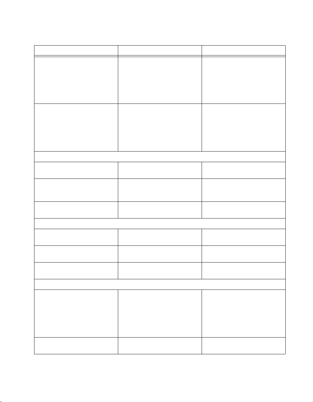
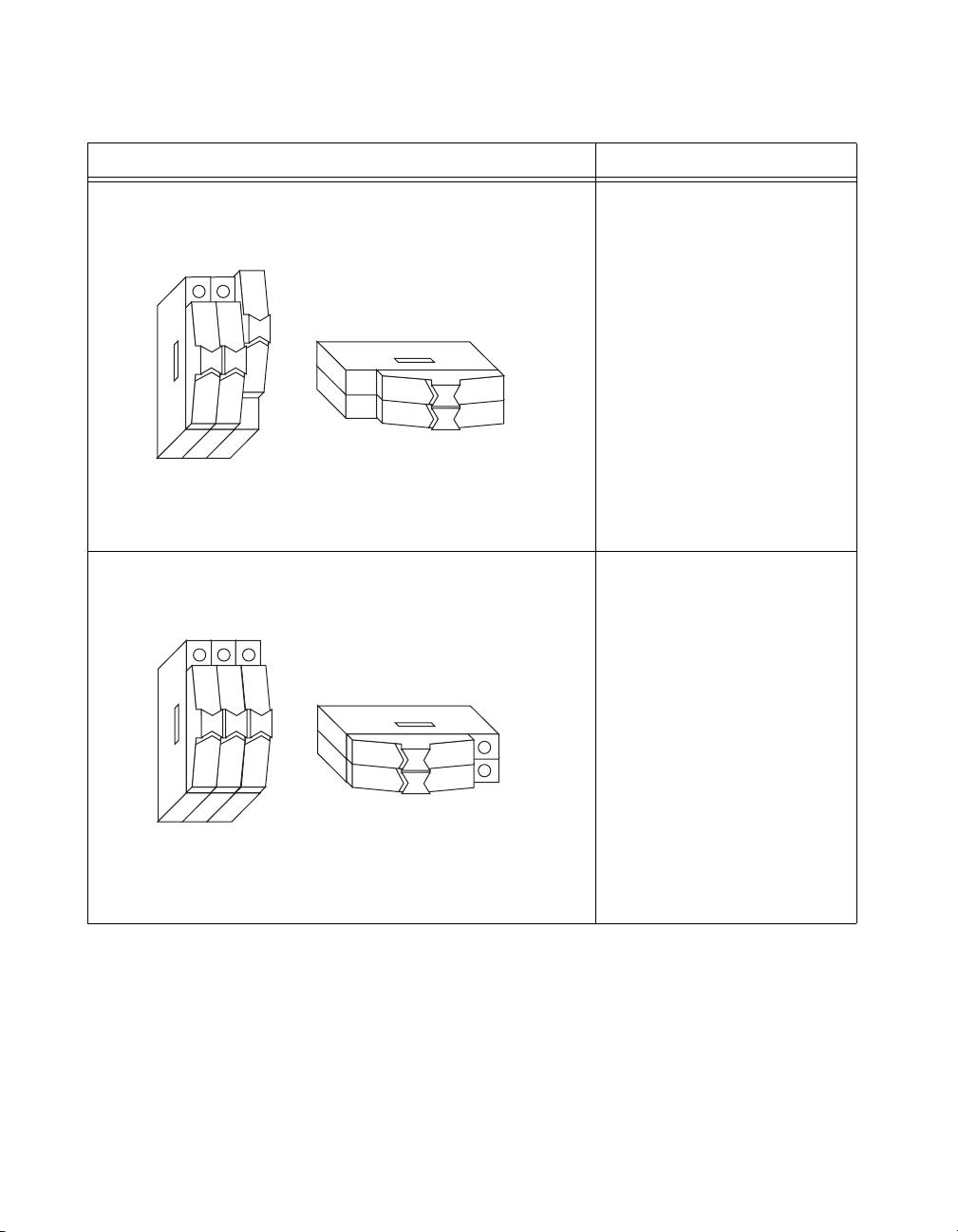
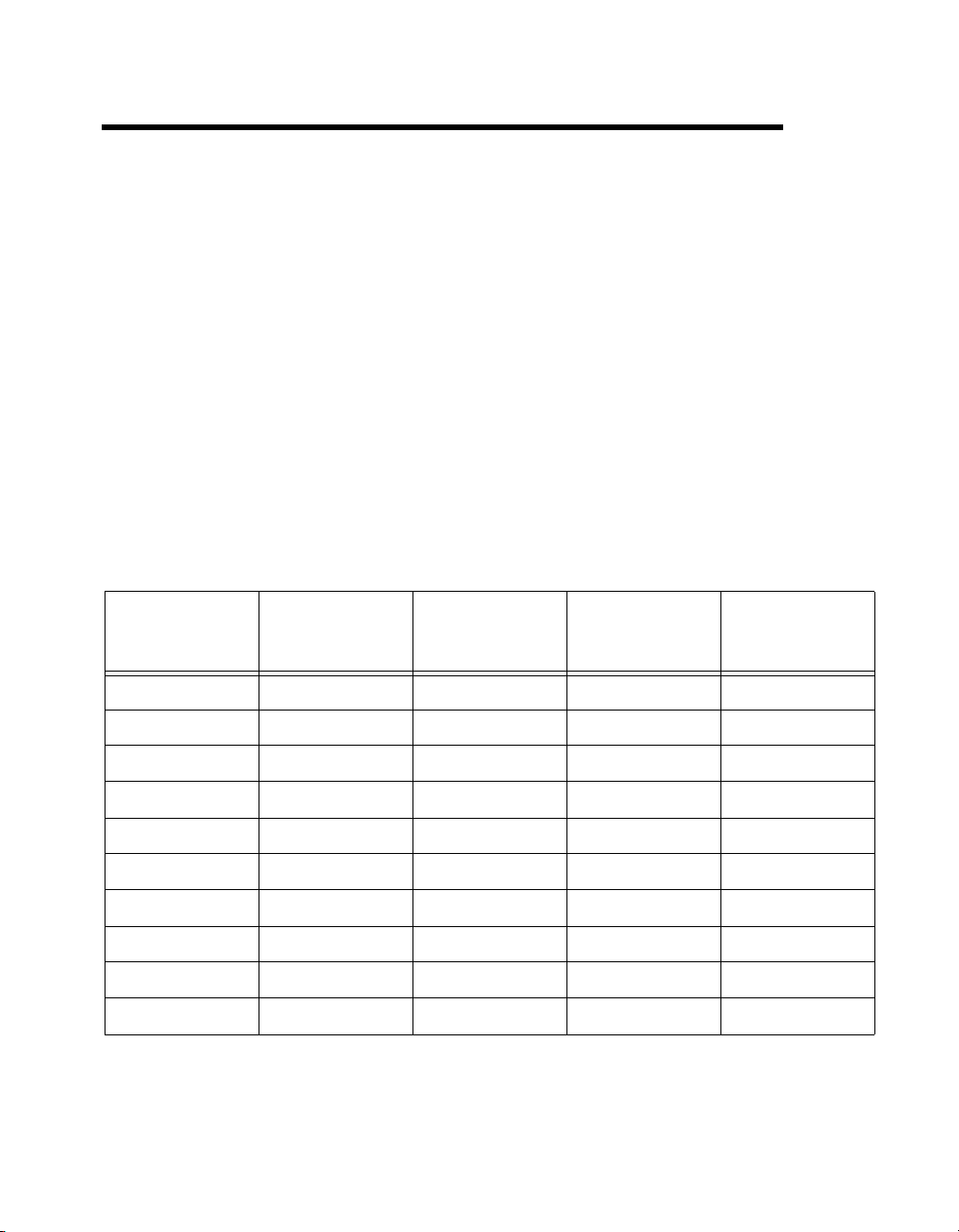
Table 1-1 shows cabling options and features for DAQ devices that are
compatible with the SCB-68. Figure 1-1 shows where to apply the quick
reference label to the inside cover of the SCB-68.
Table 1-1. Device-Specific Hardware Configuration
Device Cable Assembly Features
E Series Devices
68-Pin Devices (except DAQCards) SH68-68-EP,
SH68-68-R1-EP,
R6868
100-Pin Devices SH1006868 Direct feedthrough only
SCB-68 Shielded Connector Block User Manual 1-2 ni.com
Direct feedthrough only
Thermocouple measurements
Open thermocouple detection
Current input
Filtering
Voltage dividers
AC coupling
Thermocouple measurements
Open thermocouple detection
Current input
Filtering
Voltage dividers
AC coupling
Page 13
Device Cable Assembly Features
NI 6024E for PCMCIA
(DAQCard-6024E),
NI 6036E for PCMCIA
(DAQCard-6036E),
NI 6062E for PCMCIA
(DAQCard-6062E)
Table 1-1. Device-Specific Hardware Configuration (Continued)
SCH68-68-EP,
RC68-68
Direct feedthrough only
Thermocouple measurements
Open thermocouple detection
Current input
Filtering
Voltage dividers
AC coupling
Chapter 1 Introduction
NI 6012E for PCMCIA
(DAQCard-AI-16XE-50),
NI 6041E for PCMCIA
(DAQCard-AI-16E-4)
NI 670X
for PCI/PXI/CompactPCI
NI 671X/673X
for PCI/PXI/CompactPCI
NI 6715 for PCMCIA
(DAQCard-6715)
NI 6533
for ISA/PCI/PXI/CompactPCI
NI 6533 for PCMCIA
(DAQCard-6533),
NI 6534
for PCI/PXI/CompactPCI
NI 7030/6030E
for PCI/PXI/CompactPCI,
NI 7030/6040E
for PCI/PXI/CompactPCI
NI 7030/6533
for PCI/PXI/CompactPCI
PSHR68-68,
PR68-68F
Analog Output (AO) Devices
SH68-68-D1
R6868
SH68-68-EP
SH68-68-R1-EP
R6868
SHC68-68-EP
RC6868
Digital I/O (DIO) Devices
SH68-68-D1
R6868
PSHR68-68-D1,
PR6868F
SH68-68-D1
R6868
Real-Time (RT) Devices
SH68-68-EP
SH68-68R1-EP,
R6868
SH68-68-D1
R6868
Direct feedthrough only
Thermocouple measurements
Open thermocouple detection
Current input
Filtering
Voltage dividers
AC coupling
Direct feedthrough only
RC filtering
Direct feedthrough only
RC filtering
Direct feedthrough only
RC filtering
Direct feedthrough only
Direct feedthrough only
Direct feedthrough only
Direct feedthrough only
Thermocouple measurements
Open thermocouple detection
Current input
Filtering
Voltage dividers
AC coupling
Direct feedthrough only
© National Instruments Corporation 1-3 SCB-68 Shielded Connector Block User Manual
Page 14
Chapter 1 Introduction
Device Cable Assembly Features
Table 1-1. Device-Specific Hardware Configuration (Continued)
S Series Devices
NI 6110/6111 for PCI SH68-68-EP
NI 6115/6120
for PCI/PXI/CompactPCI
NI 6601/6602
for PCI/PXI/CompactPCI
NI 250X
for PXI/CompactPCI
NI 4350 for PCMCIA
(DAQCard-4350),
NI 4350 for USB
NI 4351
for PCI/PXI/CompactPCI
NI 445X for PCI SHC50-68 Direct feedthrough only
SH68-68R1-EP,
R6868
SH68-68-EP
SH68-68R1-EP,
R6868
Timing I/O (TIO) Devices
SH68-68-D1,
R6868
Other Devices
SH68-68 Direct feedthrough only
SH68-68 Not recommended for use with the
SH68-68 Not recommended for use with the
Direct feedthrough only
Direct feedthrough only
Direct feedthrough only
SCB-68
To maximize the available features,
NI recommends using this DAQ
device with the CB-68T, TBX-68,
or TBX-68T terminal blocks.
SCB-68
To maximize the available features,
NI recommends using this DAQ
device with the CB-68T, TBX-68,
or TBX-68T terminal blocks.
NI 455X for PCI SHC50-68 Direct feedthrough only
NI 5411
for PCI/PXI/CompactPCI
NI 5431
for PCI/PXI/CompactPCI
SCB-68 Shielded Connector Block User Manual 1-4 ni.com
SHC50-68 Direct feedthrough only
SHC50-68 Direct feedthrough only
Page 15
Chapter 1 Introduction
1
2
3
10
9
1 Quick Reference Label
2 Cover
3 68-Pin Connector
Installing Cables
The following sections describe how to cable one or more SCB-68
connector blocks to a DAQ device using 68-pin or 100-pin cables.
Note For the I/O connector pinout of the DAQ device, refer to the device user manual at
ni.com/manuals or to the quick reference label provided with the DAQ device.
Using 68-Pin Cables
Table 1-1 lists the 68-pin cable assemblies that can connect the SCB-68 to
a 68-pin DAQ device. Each end of these 68-pin cables has a 68-pin I/O
connector that you can connect to the SCB-68 and to the 68-pin DAQ
device. In this configuration, the I/O connector pinout on the DAQ device
determines the I/O connector pinout on the SCB-68.
Screws
8
7
4 Lock Washers
5 Shielding Screws
6 68-Pin I/O Connector
7Base
Figure 1-1. SCB-68 Parts Locator Diagram
5
6
8 Strain-Relief Bars
9 Strain-Relief Screws
10 Circuit Card Assembly
4
© National Instruments Corporation 1-5 SCB-68 Shielded Connector Block User Manual
Page 16
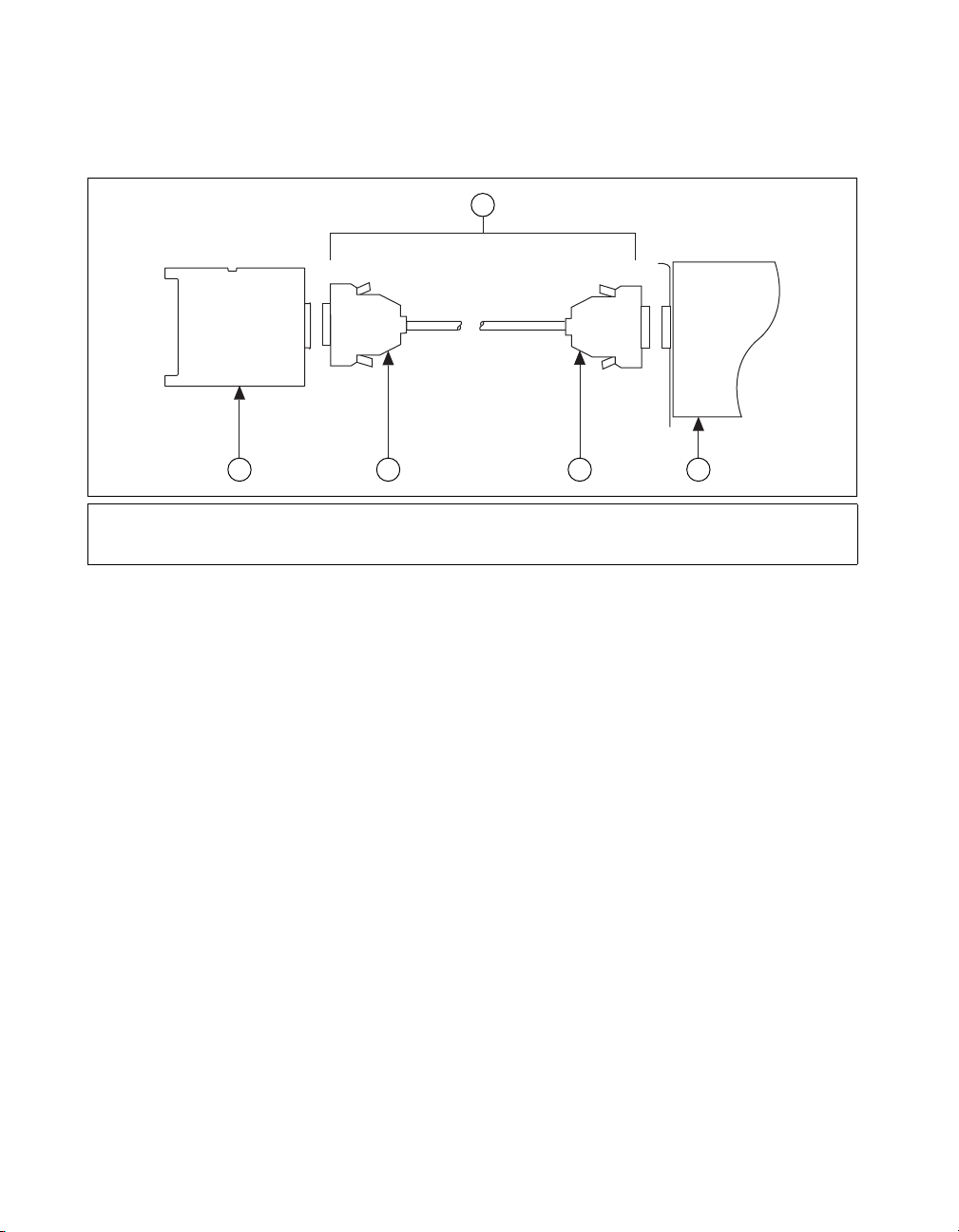
Chapter 1 Introduction
Figure 1-2 shows how to use a 68-pin cable to connect the SCB-68 to a
68-pin DAQ device.
1
5 4
1 68-Pin Cable Assembly
268-Pin DAQ Device
3 68-Pin I/O Connector
Using 100-Pin Cables
You can use the SH1006868 cable assembly to connect two SCB-68
connector blocks to a 100-pin DAQ device. The SH1006868 is Y-shaped,
with a 100-pin male connector on one end and two 68-pin female
connectors on the opposite end. The DAQ device connects to the 100-pin
cable connector, and an SCB-68 can connect to each 68-pin cable
connector. Figure 1-3 shows how use the SH1006868 to cable a 100-pin
DAQ device to two SCB-68 devices.
23
4 68-Pin I/O Connector
5 SCB-68 Connector Block
Figure 1-2. Connecting a 68-Pin DAQ Device to an SCB-68
SCB-68 Shielded Connector Block User Manual 1-6 ni.com
Page 17
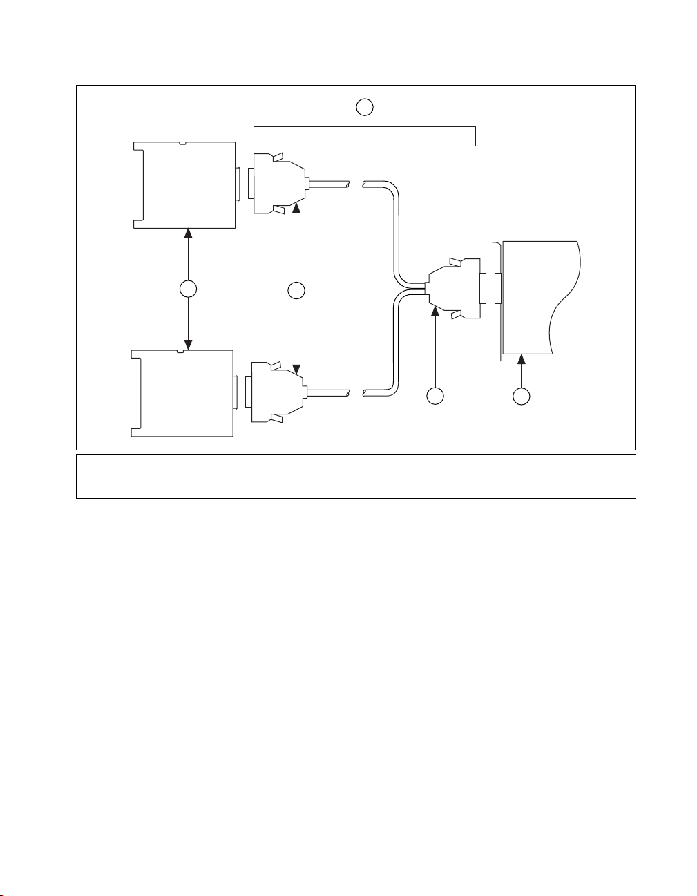
Chapter 1 Introduction
3
1
1 SCB-68 Connector Blocks
2 68-Pin I/O Connectors
3 SH1006868 Cable Assembly
When you attach two SCB-68 devices to the SH1006868 cable, one of the
SCB-68 connector blocks has a full 68-pin I/O connector pinout, and the
other SCB-68 connector block has an extended AI or extended digital
pinout. Each 68-pin end of the SH1006868 cable has a label that indicates
which I/O connector pinout is associated with that 68-pin I/O connector.
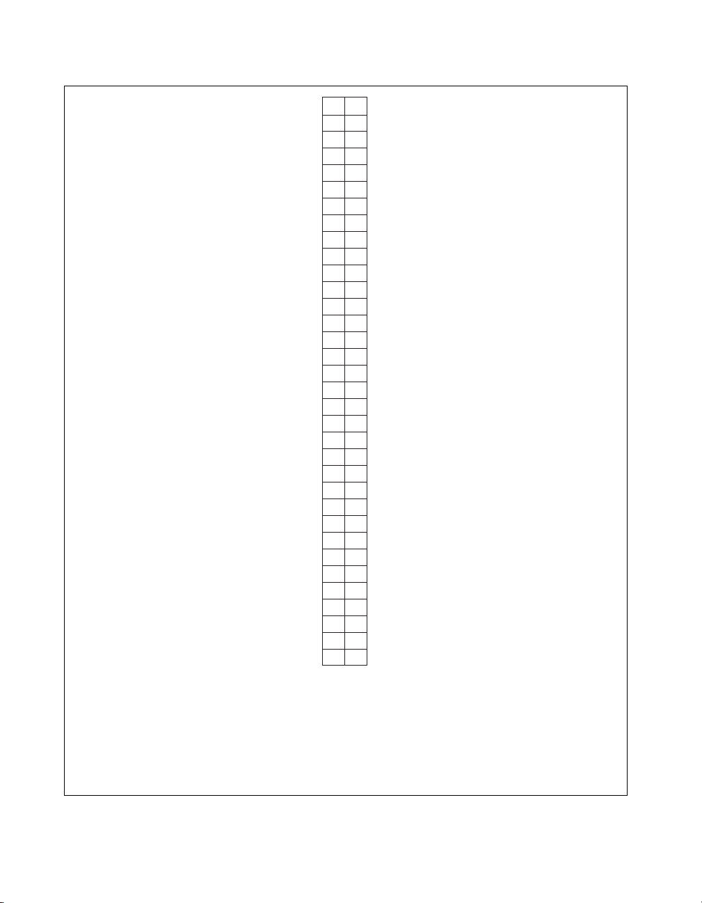
Figure 1-4 shows the pin assignments for the I/O connector on a 68-pin
E Series device. This connector is available when you use the SH68-68-EP
or R6868 cable assemblies with an E Series DAQ device. It is also one of
two 68-pin connectors available when you use the SH1006868 cable
assembly with a 100-pin E Series DAQ device.
2
5
4 100-Pin DAQ Device
5 100-Pin I/O Connector
4
Figure 1-3. Connecting a 100-Pin DAQ Device to Two SCB-68 Connector Blocks
© National Instruments Corporation 1-7 SCB-68 Shielded Connector Block User Manual
Page 18
Chapter 1 Introduction
ACH8
ACH1
AIGND
ACH10
ACH3
AIGND
ACH4
AIGND
ACH13
ACH6
AIGND
ACH15
DAC0OUT
DAC1OUT
EXTREF
DIO4
DGND
DIO1
DIO6
DGND
+5V
DGND
DGND
PFI0/TRIG1
PFI1/TRIG2
DGND
+5V
DGND
PFI5/UPDATE*
PFI6/WFTRIG
DGND
PFI9/GPCTR0_GATE
GPCTR0_OUT
FREQ_OUT
1
1
3
34 68
33 67
32 66
31 65
30 64
29 63
28 62
27 61
26 60
25 59
24 58
23 57
22 56
21 55
20 54
19 53
18 52
17 51
16 50
15 49
14 48
13 47
12 46
11 45
10 44
943
842
741
640
539
438
337
236
135
ACH0
AIGND
ACH9
ACH2
AIGND
ACH11
AISENSE
ACH12
ACH5
AIGND
ACH14
ACH7
AIGND
AOGND
AOGND
2
2
DGND
DIO0
DIO5
DGND
DIO2
DIO7
DIO3
SCANCLK
EXTSTROBE*
DGND
PFI2/CONVERT*
PFI3/GPCTR1_SOURCE
PFI4/GPCTR1_GATE
GPCTR1_OUT
DGND
PFI7/STARTSCAN
PFI8/GPCTR0_SOURCE
DGND
DGND
1
No connect on the DAQCard-AI-16E-4, DAQCard-AI-16XE-50, NI PCI-6023E, NI PCI-6032E,
NI PCI-6033E, and NI PCI-6034E
2
No connect on the DAQCard-AI-16E-4 and DAQCard-AI-16XE-50
3
No connect on the DAQCard-AI-16E-4, DAQCard-AI-16XE-50, DAQCard-6024E, NI PCI-6023E,
NI PCI-6024E, NI PXI-6030E, NI PXI-6031E, NI PCI-6032E, NI PCI-6033E, NI PCI-6034E,
NI PCI-6035E, NI PCI-6036E, PCI-MIO-16XE-10, and PCI-MIO-16XE-50
Figure 1-4. SCB-68 E Series I/O Connector Pinout (Full)
SCB-68 Shielded Connector Block User Manual 1-8 ni.com
Page 19
Chapter 1 Introduction
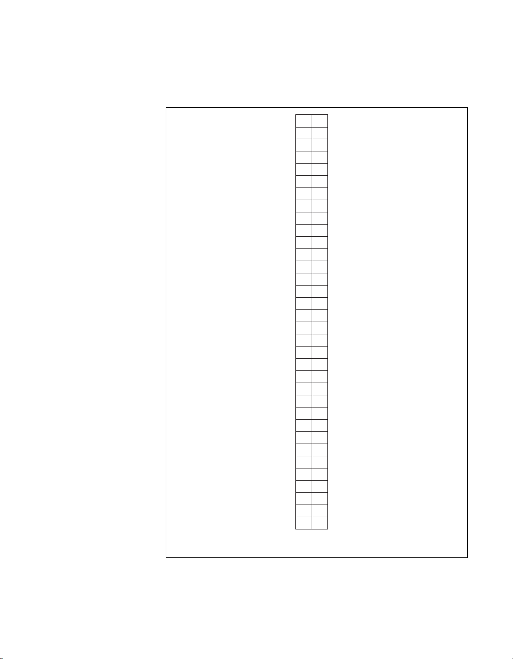
Figure 1-5 shows the pin assignments for the extended AI connector. This
pinout shows the other 68-pin connector when you use the SH1006868
cable assembly with an NI 6031E, NI 6033E, or NI 6071E.
ACH24
ACH17
ACH18
ACH27
ACH20
ACH21
ACH30
ACH23
ACH32
ACH41
ACH34
ACH35
AIGND
ACH44
ACH37
ACH38
ACH47
ACH48
ACH49
ACH58
ACH51
ACH52
ACH61
ACH54
ACH55
NC
NC
NC
NC
NC
NC
NC
NC
NC
34 68
33 67
32 66
31 65
30 64
29 63
28 62
27 61
26 60
25 59
24 58
23 57
22 56
21 55
20 54
19 53
18 52
17 51
16 50
15 49
14 48
13 47
12 46
11 45
10 44
943
842
741
640
539
438
337
236
135
ACH16
ACH25
ACH26
ACH19
ACH28
ACH29
ACH22
ACH31
ACH40
ACH33
ACH42
ACH43
AISENSE2
ACH36
ACH45
ACH46
ACH39
ACH56
ACH57
ACH50
ACH59
ACH60
ACH53
ACH62
ACH63
NC
NC
NC
NC
NC
NC
NC
NC
NC
NC = No Connect
Figure 1-5. SCB-68 E Series I/O Connector Pinout (Extended AI)
© National Instruments Corporation 1-9 SCB-68 Shielded Connector Block User Manual
Page 20
Chapter 1 Introduction
Figure 1-6 shows the pin assignments for the extended digital connector.
This pinout shows the other 68-pin connector when you use the
SH1006868 cable assembly with an NI 6025E or the NI 6021E
(AT-MIO-16DE-10) for ISA.
34 68
GND
PC6
PC5
GND
PC3
PC2
GND
PC0
PB7
GND
PB5
PB4
GND
GND
PB1
PB0
GND
PA6
PA5
GND
PA3
PA2
GND
PA0
+5V
NC
NC
NC
NC
NC
NC
NC
NC
NC
33 67
32 66
31 65
30 64
29 63
28 62
27 61
26 60
25 59
24 58
23 57
22 56
21 55
20 54
19 53
18 52
17 51
16 50
15 49
14 48
13 47
12 46
11 45
10 44
943
842
741
640
539
438
337
236
135
PC7
GND
GND
PC4
GND
GND
PC1
GND
GND
PB6
GND
GND
PB3
PB2
GND
GND
PA7
GND
GND
PA4
GND
GND
PA1
GND
GND
NC
NC
NC
NC
NC
NC
NC
NC
NC
NC = No Connect
Figure 1-6. SCB-68 E Series I/O Connector Pinout (Extended Digital)
SCB-68 Shielded Connector Block User Manual 1-10 ni.com
Page 21

Configuring the SCB-68
For instructions about using Measurement & Automation Explorer (MAX)
to configure the SCB-68 as an accessory for a DAQ device, complete the
following steps:
1. Navigate to MAX by selecting Start»Programs»National
Instruments»Measurement&Automation.
2. Select Help»Help Topics»NI-DAQ in MAX.
3. Select DAQ Devices»Configuring DAQ Devices»Configuring
DAQ Devices»Accessory in the Measurement & Automation Explorer
Help for MAX.
Safety Information
The following section contains important safety information that you must
follow when installing and using the SCB-68.
Do not operate the SCB-68 in a manner not specified in this document.
Misuse of the SCB-68 can result in a hazard. You can compromise the
safety protection built into the SCB-68 if the device is damaged in any way.
If the SCB-68 is damaged, return it to NI for repair.
Chapter 1 Introduction
Do not substitute parts or modify the SCB-68 except as described in this
document. Use the SCB-68 only with the chassis, modules, accessories,
and cables specified in the installation instructions. You must have all
covers and filler panels installed during operation of the SCB-68.
Do not operate the SCB-68 in an explosive atmosphere or where there may
be flammable gases or fumes. Operate the SCB-68 only at or below the
pollution degree stated in Appendix A, Specifications.
Pollution is foreign matter in a solid, liquid, or gaseous state that can reduce
dielectric strength or surface resistivity. The following is a description of
pollution degrees:
• Pollution Degree 1 means no pollution or only dry, nonconductive
pollution occurs. The pollution has no influence.
• Pollution Degree 2 means that only nonconductive pollution occurs in
most cases. Occasionally, however, a temporary conductivity caused
by condensation must be expected.
© National Instruments Corporation 1-11 SCB-68 Shielded Connector Block User Manual
Page 22

Chapter 1 Introduction
• Pollution Degree 3 means that conductive pollution occurs, or dry,
nonconductive pollution occurs that becomes conductive due to
condensation.
Clean the SCB-68 with a soft nonmetallic brush. Make sure that the
SCB-68 is completely dry and free from contaminants before returning it
to service.
You must insulate signal connections for the maximum voltage for which
the SCB-68 is rated. Do not exceed the maximum ratings for the SCB-68.
Remove power from signal lines before connecting them to or
disconnecting them from the SCB-68.
Operate the SCB-68 only at or below the installation category stated in
Appendix A, Specifications.
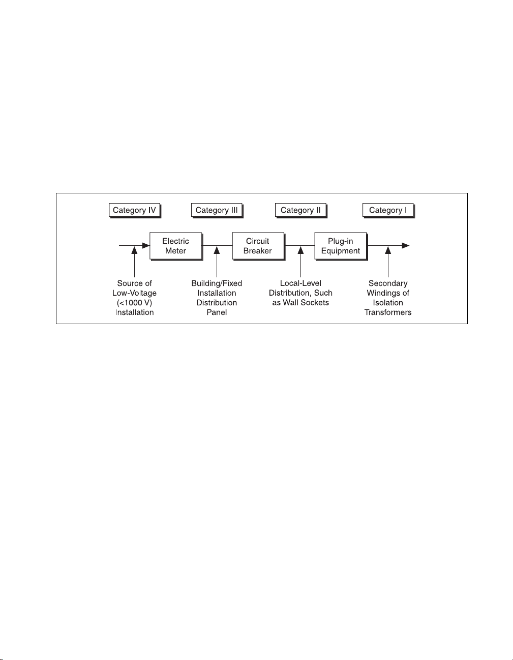
The following is a description of installation categories:
• Installation Category I is for measurements performed on circuits not
directly connected to MAINS
1
. This category is a signal level such as
voltages on a printed wire board (PWB) on the secondary of an
isolation transformer.
Examples of Installation Category I are measurements on circuits not
derived from MAINS and specially protected (internal)
MAINS-derived circuits.
• Installation Category II is for measurements performed on circuits
directly connected to the low-voltage installation. This category refers
to local-level distribution such as that provided by a standard wall
outlet.
Examples of Installation Category II are measurements on household
appliances, portable tools, and similar equipment.
• Installation Category III is for measurements performed in the building
installation. This category is a distribution level referring to hardwired
equipment that does not rely on standard building insulation.
Examples of Installation Category III include measurements on
distribution circuits and circuit breakers. Other examples of
Installation Category III are wiring including cables, bus-bars,
junction boxes, switches, socket outlets in the building/fixed
1
MAINS is defined as the electricity supply system to which the equipment concerned is designed to be connected either for
powering the equipment or for measurement purposes.
SCB-68 Shielded Connector Block User Manual 1-12 ni.com
Page 23
Chapter 1 Introduction
installation, and equipment for industrial use, such as stationary
motors with a permanent connection to the building/fixed installation.
• Installation Category IV is for measurements performed at the source
of the low-voltage (<1,000 V) installation.
Examples of Installation Category IV are electric meters, and
measurements on primary overcurrent protection devices and
ripple-control units.
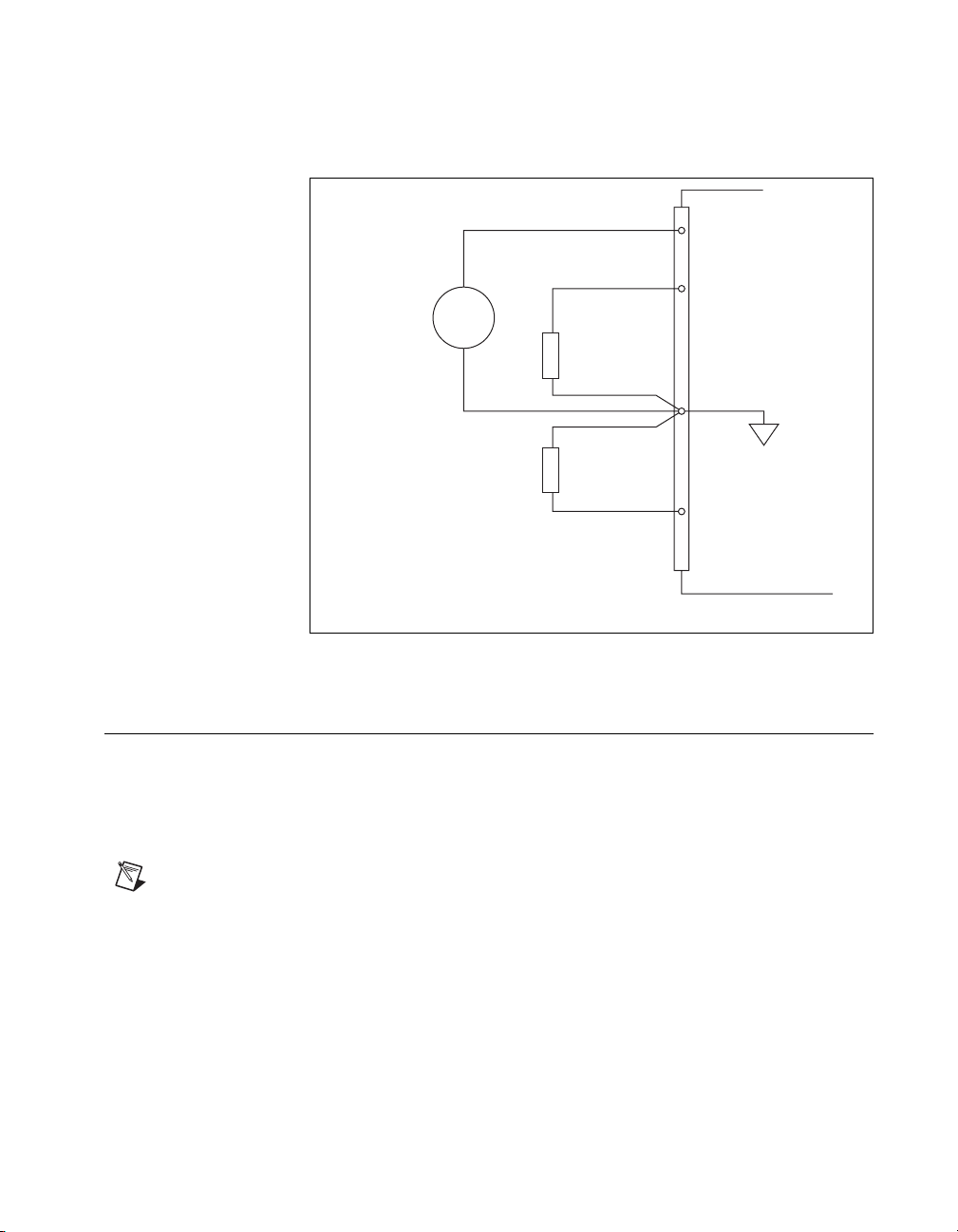
Below is a diagram of a sample installation.
© National Instruments Corporation 1-13 SCB-68 Shielded Connector Block User Manual
Page 24
Parts Locator and Wiring Guide
This chapter explains how to connect signals to the SCB-68.
The following cautions contain important safety information concerning
hazardous voltages and terminal blocks.
Cautions Keep away from live circuits. Do not remove equipment covers or shields unless
you are trained to do so. If signal wires are connected to the SCB-68, dangerous voltages
may exist even when the equipment is powered off. To avoid dangerous electrical shock,
do not perform procedures involving cover or shield removal unless you are qualified to do
so. Before you remove the cover, disconnect the AC power or any live circuits from the
SCB-68.
The chassis GND terminals are for grounding high-impedance sources such as floating
sources (1 mA maximum). Do not use these terminals as safety earth grounds.
Do not connect high voltages to the SCB-68 even with an attenuator circuit. Never connect
voltages ≥42 V
or connection.
. NI is not liable for any damage or injuries resulting from improper use
rms
2
© National Instruments Corporation 2-1 SCB-68 Shielded Connector Block User Manual
Page 25
Chapter 2 Parts Locator and Wiring Guide
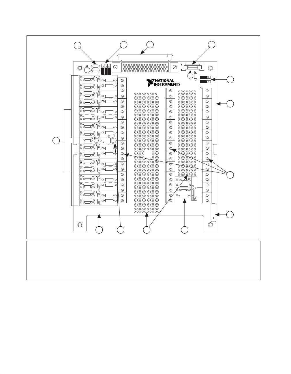
13
1
C6
R20
R21
C4
R22(A)
RC12(B)
RC4(E)
R23(C)
RC13(D)
R24(A)
RC14(B)
RC5(E)
R25(C)
RC15(D)
R26(A)
RC16(B)
RC6(E)
R27(C)
RC17(D)
R28(A)
RC18(B)
RC7(E)
R29(C)
C5
RC19(D)
R38
R30(A)
RC20(B)
RC8(E)
R31(C)
RC21(D)
R32(A)
RC22(B)
RC9(E)
R33(C)
RC23(D)
R34(A)
RC24(B)
RC10(E)
R35(C)
RC25(D)
R36(A)
RC26(B)
RC11(E)
R37(C)
RC27(D)
SCB-68
COPYRIGHT 1993
©
2
33
S4 S3
R4(F)
R5(G)
R6(F)
R7(G)
R8(F)
R9(G)
R10(F)
R11(G)
C3
R12(F)
R13(G)
R14(F)
R15(G)
R16(F)
R17(G)
R18(F)
R19(G)
34
68
34
67
33
66
32
65
31
64
30
63
29
62
28
61
27
60
26
59
25
58
24
57
23
S5
3 4
1
J1
3
C2
C1
12
46
13
47
14
48
15
49
16
50
17
51
18
52
19
53
20
54
21
55
22
RC2
R2
RC3
R3
RC1
R10
56
XF1
S1
S2
5
ASSY182470-01 REV.B
1
35
2
36
6
3
37
4
38
5
39
6
40
7
41
8
42
9
43
7
10
44
11
45
S/N
8
1 Pads R20 and R21
2 Switches S3, S4, and S5
3 68-Pin I/O Connector
4 Fuse (0.8 A)
5 Switches S1 and S2
6 Assembly Number and Revision Letter
7 Screw Terminals
101112
8 Serial Number
9 RC Filters and Attenuators for DAC0,
DAC1, and TRIG1
10 Breadboard Area
11 Temperature Sensor
12 Product Name
13 Pads for AI Conditioning
9
Figure 2-1. SCB-68 Printed Circuit Diagram
SCB-68 Shielded Connector Block User Manual 2-2 ni.com
Page 26

Chapter 2 Parts Locator and Wiring Guide
To connect signals to the SCB-68, complete the following steps while
referring to Figure 1-1, SCB-68 Parts Locator Diagram, and to Figure 2-1.
1. Disconnect the 68-pin cable from the SCB-68, if it is connected.
2. Remove the shielding screws on either side of the top cover with a
Phillips-head number 1 screwdriver. You can now open the box.
3. Configure the switches and other options relative to the types of signals
you are using.
4. Loosen the strain-relief screws with a Phillips-head number 2
screwdriver. Slide the signal wires through the front panel strain-relief
opening. You can also remove the top strain-relief bar if you are
connecting many signals. Add insulation or padding if necessary.
5. Connect the wires to the screw terminals by stripping off 0.25 in. of the
insulation, inserting the wires into the green terminals, and tightening
the screws.
6. Reinstall the strain-relief bar (if you removed it) and tighten the
strain-relief screws.
7. Close the top cover.
8. Reinsert the shielding screws to ensure proper shielding.
You can now connect the SCB-68 to the 68-pin I/O connector.
Switch Configuration
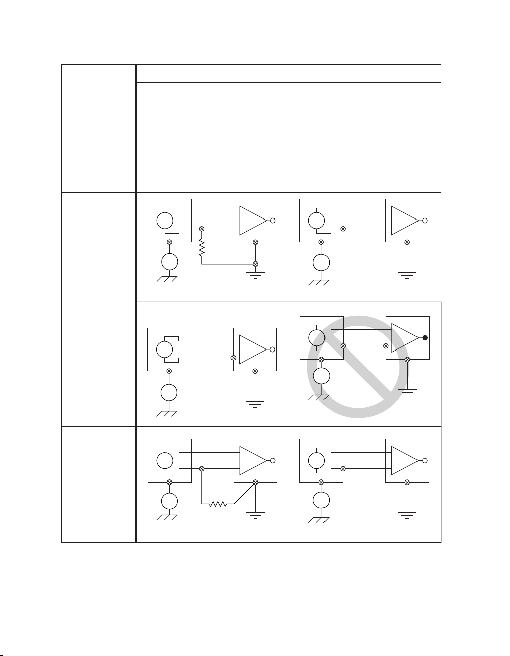
The SCB-68 has five switches that must be properly configured to use the
SCB-68 with the DAQ device. Table 2-1 illustrates the available switch
configurations and the affected signals for each switch setting. Refer to
Table 2-1 to determine the switch setting that applies to your application,
and then refer to the following sections for more information on specific
types of signals.
© National Instruments Corporation 2-3 SCB-68 Shielded Connector Block User Manual
Page 27
Chapter 2 Parts Locator and Wiring Guide
Table 2-1. Switch Configurations and Affected Signals
Switch Setting Applicable Signals
Temperature Sensor
S5 S4 S3
Signal Conditioning
Circuitry Power (Off)
S1
S2
Direct feedthrough, with temperature sensor disabled and
accessory power disabled
Temperature Sensor
S5 S4 S3
Signal Conditioning
Circuitry Power (On)
S1
S2
Analog input, analog output,
digital I/O, and timing I/O
Analog input
and analog output
1
Temperature sensor disabled, and accessory power enabled
2
Note: This configuration is the factory-default configuration.
SCB-68 Shielded Connector Block User Manual 2-4 ni.com
Page 28
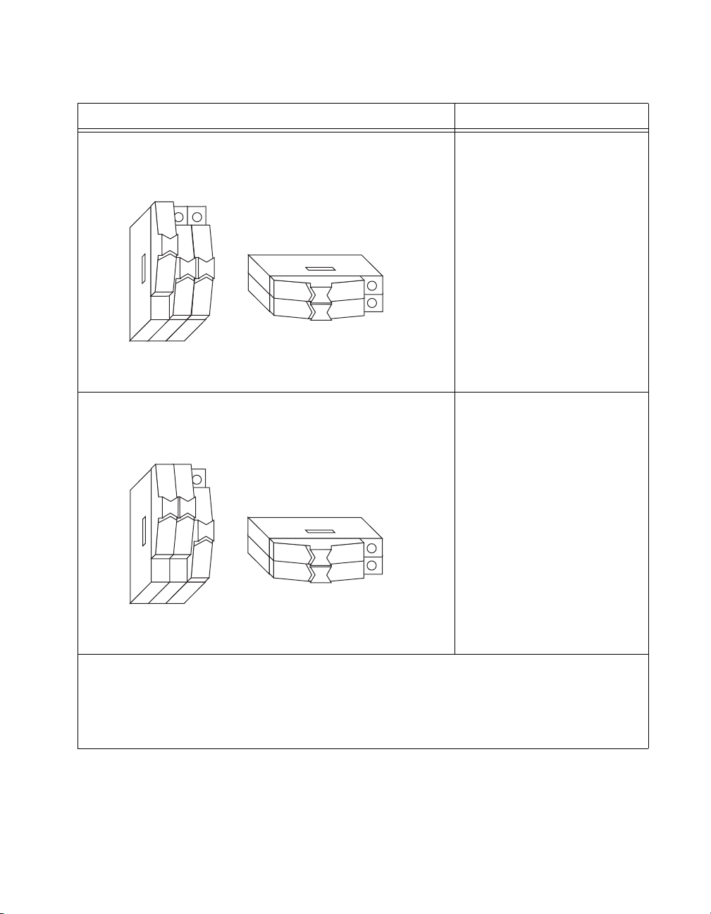
Table 2-1. Switch Configurations and Affected Signals (Continued)
Temperature Sensor
S5 S4 S3
Chapter 2 Parts Locator and Wiring Guide
Switch Setting Applicable Signals
Signal Conditioning
Circuitry Power (On)
S1
S2
Single-ended analog input
3
Single-ended temperature sensor, with accessory power enabled
Temperature Sensor
S5 S4 S3
Signal Conditioning
Circuitry Power (On)
S1
S2
Differential temperature sensor, with accessory power enabled
1
When accessory power is enabled, I/O pin 8 is fused and is intended to be connected to +5V. This setting is not
recommended for use with the NI 653X, NI 670X, or NI 660X. Refer to the device user manual at
determine if the device supplies +5 V to I/O pin 8.
2
Only applies to the signal conditioning circuitry.
3
Except NI 61XX devices. Refer to the device user manual at ni.com/manuals to determine if the device supports
single-ended inputs.
2
Differential analog input
2
ni.com/manuals to
© National Instruments Corporation 2-5 SCB-68 Shielded Connector Block User Manual
Page 29

Connecting Signals
This chapter describes the types of signal sources that you use when
configuring the channels and making signal connections to the SCB-68,
describes input modes, and discusses noise considerations to help you
acquire accurate signals.
Connecting Analog Input Signals
The following sections describe how to connect signal sources for
single-ended or differential (DIFF) input mode. On most devices, you can
software-configure the DAQ device channels for two types of single-ended
connections—nonreferenced single-ended (NRSE) input mode and
referenced single-ended (RSE) mode. RSE input mode is used for floating
signal sources. In this case, the DAQ device provides the reference
ground point for the external signal. NRSE input mode is used for
ground-referenced signal sources. In this case, the external signal supplies
its own reference ground point, and the DAQ device should not supply one.
Note Some devices might only support one of the possible input modes.
3
Input Modes
You can configure the DAQ device for one of three input modes—NRSE,
RSE, or DIFF. The following sections discuss the use of single-ended and
differential measurements and considerations for measuring both floating
and ground-referenced signal sources. On devices that support both
single-ended and DIFF input modes, using DIFF input mode commits two
channels, ACH<i> and ACH<i+8>, to each signal. Figure 3-1 summarizes
the recommended input modes for both types of signal sources.
© National Instruments Corporation 3-1 SCB-68 Shielded Connector Block User Manual
Page 30
Chapter 3 Connecting Signals
Signal Source Type
Input
Differential
(DIFF)
Single-Ended —
Ground
Referenced
(RSE)
Floating Signal Source
(Not Connected to Building Ground)
Examples:
• Ungrounded thermocouples
• Signal conditioning with
Isolated outputs
• Battery devices
Common-
Mode
Voltage
Refer to the
+
V
–
ACH(+)
1
ACH(–)
R
+
–
Using Bias Resistors
+
–
AIGND
section for information on bias resistors.
Common-
Mode
Voltage
+
V
–
ACH
1
AIGND
+
–
+
–
Grounded Signal Source
Examples:
• Plug-in instruments with
nonisolated outputs
ACH(+)
1
ACH(–)
Common-
Mode
Voltage
+
V
–
+
–
NOT RECOMMENDED
ACH
1
+ V
–
g
Common-
Mode
Voltage
+
V
–
+
–
Ground-loop losses, Vg, are added to
measured signal.
+
–
AIGND
+
–
AIGND
ACH
+
V
1
–
AISENSE
+
–
+
V
–
ACH
1
AISENSE
+
–
Single-Ended —
Nonreferenced
(NRSE)
Common-
Mode
Voltage
Refer to the
+
–
Using Bias Resistors
R
AIGND
Common-
Mode
Voltage
+
–
AIGND
section for information on bias resistors.
Figure 3-1. Summary of AI Connections
SCB-68 Shielded Connector Block User Manual 3-2 ni.com
Page 31

Nonreferenced or Floating Signal Sources
A floating signal source is a signal source that is not connected in any way
to the building ground system, but has an isolated ground-reference point.
Instruments or devices with isolated outputs are considered floating signal
sources, and they have high-impedance paths to ground. Some examples of
floating signal sources are outputs for thermocouples, transformers,
battery-powered devices, optical isolators, and isolation amplifiers. The
ground reference of a floating source must be tied to the ground of the DAQ
device to establish a local or onboard reference for the signal. Otherwise,
the measured input signal varies as the source floats outside the
common-mode input range.
Differential Inputs
When measuring differential floating sources, you must configure the
device for DIFF input mode. To provide a return path for the
instrumentation amplifier bias currents, differential floating sources must
have a 10 to 100 kΩ resistor connected to AIGND on one input if they are
DC coupled or on both inputs if sources are AC coupled. You can install
bias resistors in positions B and D of the SCB-68, as shown in Figure 5-1,
Analog Input Channel Configuration Diagram for ACH<i> and
ACH<i+8>.
Chapter 3 Connecting Signals
Single-Ended Inputs
When measuring single-ended floating signal sources, you must configure
the DAQ device to supply a ground reference by configuring the DAQ
device for RSE input mode. In this mode, the negative input of the
instrumentation amplifier on the DAQ device is tied to the analog ground.
To use the SCB-68 with single-ended inputs, where ACH<i> and
ACH<i+8> are used as two single-ended channels, configure the SCB-68
in its factory-default configuration. In the factory-default configuration,
jumpers on the SCB-68 are in the two series positions, F and G, as shown
in Figure 5-1, Analog Input Channel Configuration Diagram for ACH<i>
and ACH<i+8>. In this configuration, you should connect all signal
grounds to AIGND.
Note Some versions of the SCB-68 use hardwired 0 Ω resistors as the factory-default
jumpers. In such cases, to move these jumpers to and from the factory-default positions,
you must solder and desolder on the SCB-68 circuit card assembly. When soldering, refer
to Appendix E, Soldering and Desoldering on the SCB-68.
© National Instruments Corporation 3-3 SCB-68 Shielded Connector Block User Manual
Page 32

Chapter 3 Connecting Signals
Ground-Referenced Signal Sources
A grounded signal source is connected in some way to the building system
ground; therefore, the signal source is already connected to a common
ground point with respect to the DAQ device (assuming that the host
computer is plugged into the same power system). Nonisolated outputs of
instruments and devices that plug into the building power system fall into
this category.
The difference in ground potential between two instruments connected to
the same building power system is typically between 1 and 100 V, but the
difference can be much greater if the power distribution circuits are
improperly connected. If a grounded signal source is incorrectly measured,
this difference may appear as a measurement error. The connection
instructions for grounded signal sources are designed to eliminate this
ground potential difference from the measured signal.
Differential Inputs
If the DAQ device is configured for DIFF input mode, where ACH<i> and
ACH<i+8> are used as a single differential channel pair, ground-referenced
signal sources connected to the SCB-68 need no special components. You
can leave the inputs of the SCB-68 in the factory configuration with the
jumpers in the two series positions, F and G. Refer to Figure 5-1, Analog
Input Channel Configuration Diagram for ACH<i> and ACH<i+8>, for a
diagram of this configuration.
Note Some versions of the SCB-68 use hardwired 0 Ω resistors as the factory-default
jumpers. In such cases, to move these jumpers to and from the factory-default positions,
you must solder and desolder on the SCB-68 circuit card assembly. When soldering, refer
to Appendix E, Soldering and Desoldering on the SCB-68.
Single-Ended Inputs
When you measure ground-referenced single-ended signals, the external
signal supplies its own reference ground point, and the DAQ device should
not supply one. Therefore, you should configure the DAQ device for NRSE
input mode. In this input mode, connect all the signal grounds to AISENSE
pin, which connects to the negative input of the instrumentation amplifier
on the DAQ device. RSE input mode is not recommended for grounded
signal sources.
To leave the SCB-68 inputs in the factory configuration with jumpers in the
series position (F or G, depending on the channel), do not use the open
positions that connect the input to AIGND, A, and C (refer to Figure 5-1,
SCB-68 Shielded Connector Block User Manual 3-4 ni.com
Page 33

Chapter 3 Connecting Signals
Analog Input Channel Configuration Diagram for ACH<i> and
ACH<i+8>). Any signal conditioning circuitry requiring a ground
reference should be built in the custom breadboard area using AISENSE as
the ground reference instead of building the circuitry in the open
component positions. Referencing the signal to AIGND can cause
inaccurate measurements resulting from an incorrect ground reference.
Note Some versions of the SCB-68 use hardwired 0 Ω resistors as the factory-default
jumpers. In such cases, to move these jumpers to and from the factory-default positions,
you must solder and desolder on the SCB-68 circuit card assembly. When soldering, refer
to Appendix E, Soldering and Desoldering on the SCB-68.
Differential Connection Considerations (DIFF Input Mode)
A differential connection is one in which the DAQ device AI signal has its
own reference signal, or signal return path. These connections are available
when the selected channel is configured in DIFF input mode. The input
signal is tied to the positive input of the instrumentation amplifier, and its
reference signal, or return, is tied to the negative input of the
instrumentation amplifier. On DAQ devices that support both single-ended
and DIFF input modes, using DIFF input mode commits two channels,
ACH<i> and ACH<i+8>, to each signal.
You should use differential input connections for any channel that meets
any of the following conditions:
• The input signal is low-level (less than 1 V).
• The leads connecting the signal to the DAQ device are longer than
10 ft (3 m).
• The input signal requires a separate ground-reference point or return
signal.
• The signal leads travel through noisy environments.
Differential signal connections reduce noise pickup and increase
common-mode noise rejection. Differential signal connections also
allow input signals to float within the common-mode limits of the
instrumentation amplifier.
© National Instruments Corporation 3-5 SCB-68 Shielded Connector Block User Manual
Page 34

Chapter 3 Connecting Signals
Ground-
Referenced
Signal
Source
+
V
s
–
Differential Connections for Ground-Referenced Signal Sources
Figure 3-2 shows how to connect a ground-referenced signal source to a
channel on the DAQ device configured in DIFF input mode.
ACH+ or ACH<i>
Instrumentation
Amplifier
+
ACH– or ACH<
i
+8>
PGIA
–
V
m
+
Measured
Voltage
–
Common-
Mode
Noise and
Ground
Potential
+
V
cm
–
I/O Connector
AISENSE*
AIGND
Measurement Device Configured in DIFF Input Mode
*AISENSE is not present on all devices.
Figure 3-2. Differential Input Connections for Ground-Referenced Signals
With this connection type, the instrumentation amplifier rejects both the
common-mode noise in the signal and the ground potential difference
between the signal source and the DAQ device ground, shown as V
cm
in
Figure 3-2.
SCB-68 Shielded Connector Block User Manual 3-6 ni.com
Page 35

Floating
Signal
Source
V
s
+
–
Bias
Resistor
(see text)
Chapter 3 Connecting Signals
Differential Connections for Nonreferenced or Floating Signal Sources
Figure 3-3 shows how to connect a floating signal source to a channel on
the DAQ device configured in DIFF input mode.
ACH+ or ACH<i>
Instrumentation
Amplifier
+
ACH– or ACH<
AISENSE*
i
+8>
PGIA
–
V
m
+
Measured
Voltage
–
AIGND
I/O Connector
Measurement Device Configured in DIFF Input Mode
*AISENSE is not present on all devices.
Figure 3-3. Differential Input Connections for Nonreferenced Signals
Using Bias Resistors
Figure 3-3 shows a bias resistor connected between ACH– or ACH<i+8>,
and AIGND. This resistor provides a return path for the ±200 pA bias
current. A value of 10 kΩ to 100 kΩ is usually sufficient. If you do not use
the resistor and the source is truly floating, the source is not likely to remain
within the common-mode signal range of the PGIA, and the PGIA
saturates, causing erroneous readings. You must reference the source to the
respective channel ground.
© National Instruments Corporation 3-7 SCB-68 Shielded Connector Block User Manual
Page 36

Chapter 3 Connecting Signals
Common-mode rejection might be improved by using another bias resistor
between ACH+ or ACH<i>, and AIGND. This connection creates a slight
measurement error caused by the voltage divider formed with the output
impedance of the floating source, but it also gives a more balanced input
for better common-mode rejection.
Single-Ended Connection Considerations
A single-ended connection is one in which the DAQ device AI signal is
referenced to a ground that can be shared with other input signals. The input
signal is tied to the positive input of the instrumentation amplifier, and the
ground is tied to the negative input of the instrumentation amplifier.
You can use single-ended input connections for input signals that meet the
following conditions:
• The input signal is high-level (greater than 1 V).
• The leads connecting the signal to the DAQ device are less than
10 ft (3 m).
• The input signal can share a common reference point with other
signals.
DIFF input connections are recommended for greater signal integrity for
any input signal that does not meet the preceding conditions.
In single-ended modes, more electrostatic and magnetic noise couples into
the signal connections than in differential modes. The coupling is the result
of differences in the signal path. Magnetic coupling is proportional to the
area between the two signal conductors. Electrical coupling is a function of
how much the electric field differs between the two conductors.
SCB-68 Shielded Connector Block User Manual 3-8 ni.com
Page 37

Chapter 3 Connecting Signals
Single-Ended Connections for Floating Signal Sources (RSE Input Mode)
Figure 3-4 shows how to connect a floating signal source to a channel on
the DAQ device configured for RSE input mode.
Floating
Signal
Source
+
V
s
–
I/O Connector
ACH
AISENSE*
AIGND
Measurement Device Configured in RSE Input Mode
*Not all devices support RSE input mode.
Figure 3-4. Single-Ended Input Connections for Nonreferenced or Floating Signals
Instrumentation
Amplifier
+
PGIA
–
V
m
+
Measured
Voltage
–
Single-Ended Connections for Grounded Signal Sources (NRSE Input Mode)
To measure a grounded signal source with a single-ended configuration,
configure the DAQ device in NRSE input mode. The signal is then
connected to the positive input of the DAQ device instrumentation
amplifier, and the signal local ground reference is connected to the negative
input of the instrumentation amplifier. The ground point of the signal
should, therefore, be connected to AISENSE. Any potential difference
between the DAQ device ground and the signal ground appears as a
common-mode signal at both the positive and negative inputs of the
instrumentation amplifier, and this difference is rejected by the amplifier.
If the input circuitry of a DAQ device were referenced to ground, in this
situation (as in the RSE input mode), this difference in ground potentials
would appear as an error in the measured voltage.
© National Instruments Corporation 3-9 SCB-68 Shielded Connector Block User Manual
Page 38

Chapter 3 Connecting Signals
Figure 3-5 shows how to connect a grounded signal source to a channel on
the DAQ device configured for NRSE input mode.
Ground-
Referenced
Signal
Source
Common-
Mode
Noise
and Ground
Potential
+
V
s
–
+
V
cm
–
I/O Connector
ACH
AISENSE*
AIGND
Measurement Device Configured in NRSE Input Mode
*Not all devices support NRSE input mode.
Figure 3-5. Single-Ended Input Connections for Ground-Referenced Signals
Connecting Analog Output Signals
When using the SCB-68 with a 68-pin or 100-pin DAQ device, the AO
signals are DAC0OUT, DAC1OUT, EXTREF, and AOGND. DAC0OUT
is the voltage output channel for AO channel 0. DAC1OUT is the voltage
output channel for AO channel 1. EXTREF is the external reference input
for both AO channels. AOGND is the ground reference signal for both AO
channels and the external reference signal.
Instrumentation
Amplifier
+
PGIA
–
V
m
+
Measured
Voltage
–
Note For more information, refer to the device user manual at ni.com/manuals for
detailed signal connection information for AO signals.
SCB-68 Shielded Connector Block User Manual 3-10 ni.com
Page 39
Chapter 3 Connecting Signals
Figure 3-6 shows how to make AO connections and the external reference
connection to the SCB-68 and the DAQ device.
EXTREF
External
Reference
Signal
(optional)
V
Connecting Digital Signals
When using the SCB-68 with a 68-pin or 100-pin DAQ device, the DIO
signals are DIO<0..7> and DGND. DIO<0..7> are the eight single-ended
DIO lines, and DGND is the ground reference. You can program all lines
individually to be inputs or outputs.
+
ref
–
Load
Load
VOUT 0
VOUT 1
+
–
–
+
Figure 3-6. Connecting AO Signals
DAC0OUT
AOGND
DAC1OUT
SCB-68
Note For more information, refer to the device user manual at ni.com/manuals for
detailed signal description and connection information.
Figure 3-7 illustrates several common DIO applications and signal
connections. Digital input applications include receiving TTL signals and
sensing external device states such as the state of the switch shown in
Figure 3-7. Digital output applications include sending TTL signals and
driving external devices such as the LED shown in Figure 3-7.
© National Instruments Corporation 3-11 SCB-68 Shielded Connector Block User Manual
Page 40

Chapter 3 Connecting Signals
+5 V
LED
DIO<4..7>
+5 V
Switch
Connecting Timing Signals
If you are using a 68-pin or 100-pin DAQ device, all external control over
device timing is routed through the programmable function input (PFI)
lines <0..9>. These PFI lines are bidirectional; as outputs they are not
programmable and reflect the state of many DAQ, waveform generation,
and general-purpose timing signals. The remaining timing signals use
five different dedicated outputs.
TTL Signal
DGND
I/O Connector
Figure 3-7. Digital I/O Connections
DIO<0..3>
SCB-68
Note For more information, refer to the device user manual at ni.com/manuals for
detailed signal description and connection information.
SCB-68 Shielded Connector Block User Manual 3-12 ni.com
Page 41

Chapter 3 Connecting Signals
All digital timing connections are referenced to DGND. Figure 3-8
demonstrates how to connect two external timing signals to the PFI pins of
a DAQ device.
PFI0
PFI2
PFI0
Source
PFI2
Source
Noise Considerations
Environmental noise can seriously affect the measurement accuracy of
your application if you do not take proper care when running signal
wires between signal sources and the device. The following
recommendations apply mainly to AI signal routing to the device,
although they also apply to signal routing in general.
Minimize noise pickup and maximize measurement accuracy by taking
the following precautions:
• Use differential AI connections to reject common-mode noise, if
the DAQ device that you are using supports DIFF input mode.
• Use individually shielded, twisted-pair wires to connect AI signals
to the device. With this type of wire, the signals attached to the
DGND
I/O Connector
SCB-68
Figure 3-8. Timing I/O Connections
© National Instruments Corporation 3-13 SCB-68 Shielded Connector Block User Manual
Page 42

Chapter 3 Connecting Signals
ACH+ and ACH– inputs are twisted together and then covered with
a shield. You then connect this shield at only one point to the signal
source ground. This kind of connection is required for signals
traveling through areas with large magnetic fields or high
electromagnetic interference.
• Route signals to the device carefully. Keep cabling away from
noise sources. A common noise source in DAQ applications is the
computer monitor. Separate the monitor from the analog signals as
far as possible.
The following recommendations apply for all signal connections to the
DAQ device:
• Separate DAQ device signal lines from high-current or
high-voltage lines. These lines can induce currents in or voltages on
the DAQ device signal lines if they run in parallel paths at a close
distance. To reduce the magnetic coupling between lines, separate
them by a reasonable distance if they run in parallel, or run the lines
at right angles to each other.
• Do not run signal lines through conduits that also contain power
lines.
• Protect signal lines from magnetic fields caused by electric motors,
welding equipment, breakers, or transformers by running them
through special metal conduits.
For information about minimizing noise in your application, refer to the
NI Developer Zone tutorial, Field Wiring and Noise Considerations for
Analog Signals, located at
SCB-68 Shielded Connector Block User Manual 3-14 ni.com
ni.com/zone.
Page 43
Using Thermocouples
This chapter describes how to take thermocouple measurements using the
SCB-68. A thermocouple is created when two dissimilar metals touch, and
the contact produces a small voltage that changes as a function of
temperature. By measuring the voltage of a thermocouple, you can
determine temperature using a nonlinear equation that is unique to each
thermocouple type. Thermocouple types are designated by capital letters
that indicate their composition according to the American National
Standards Institute (ANSI) conventions. To determine the type of
thermocouple that you are using, refer to Table 4-1. For more information
on the theory of operation of thermocouples, refer to the NI Developer
Zone tutorial, Measuring Temperature with Thermocouples, at
ni.com/zone.
Table 4-1. Thermocouple Coloring
Thermocouple
Type
Positive Color Negative Color
Thermocouple
Cover Color
4
Extended
Grade Cover
Color
B Gray Red — Gray
C White/Red Trace Red — White/Red Trace
E Purple Red Brown Purple
J White Red Brown Black
K Yellow Red Brown Yellow
N Orange Red Brown Orange
R Black Red — Green
S Black Red — Green
U Black Red — Green
T Blue Red Brown Blue
© National Instruments Corporation 4-1 SCB-68 Shielded Connector Block User Manual
Page 44

Chapter 4 Using Thermocouples
The maximum voltage level thermocouples generate is typically only a few
millivolts. Therefore, you should use a DAQ device with high gain for best
resolution. You can measure thermocouples in either differential or
single-ended configuration. The differential configuration has better noise
immunity, but the single-ended configurations have twice as many inputs.
The DAQ device must have a ground reference, because thermocouples are
floating signal sources. Therefore, use bias resistors if the DAQ device is in
DIFF input mode. For a single-ended configuration, use RSE input mode.
For more information on field wiring considerations, refer to the
NI Developer Zone tutorial, Field Wiring and Noise Considerations for
Analog Signals, located at
Cold-junction compensation (CJC) with the SCB-68 is accurate only if the
temperature sensor reading is close to the actual temperature of the screw
terminals. When you read thermocouple measurements, keep the SCB-68
away from drafts or other temperature gradients, such as those caused by
heaters, radiators, fans, and very warm equipment. To minimize
temperature gradients, keep the cover of the SCB-68 closed and add custom
insulation, such as foam tape, to the SCB-68.
ni.com/zone.
Switch Settings and Temperature Sensor Configuration
To accommodate thermocouples with DAQ devices, the SCB-68 has a
temperature sensor for CJC. To power the temperature sensor, set switches
S1, S2, and S3 as shown in Figures 4-1 and 4-2. Notice that this
configuration also powers on the signal conditioning accessory power.
Signal conditioning accessories include temperature sensors and signal
conditioning circuitry.
For single-ended operation, connect referenced single-ended analog
channel 0 to the temperature sensor by switching S5 to the up position.
The signal is referenced to AIGND. Set the switches as shown in
Figure 4-1.
SCB-68 Shielded Connector Block User Manual 4-2 ni.com
Page 45

Chapter 4 Using Thermocouples
Temperature Sensor
S5 S4 S3
Signal Conditioning
Circuitry Power (On)
S1
S2
Figure 4-1. Single-Ended Switch Configuration
For differential operation, connect differential analog channel 0 to the
temperature sensor by switching S5 and S4 to the up position, as shown in
Figure 4-2.
Temperature Sensor
S5 S4 S3
Signal Conditioning
Circuitry Power (On)
S1
S2
Figure 4-2. Differential Switch Configuration
Special Considerations
To connect a high-value resistor between the positive input and +5V, refer
to the Accuracy and Resolution Considerations section of Chapter 5,
Adding Components for Special Functions.
To reduce noise by connecting a lowpass filter to the analog inputs of the
SCB-68, refer to the Lowpass Filtering section of Chapter 5, Adding
Components for Special Functions.
© National Instruments Corporation 4-3 SCB-68 Shielded Connector Block User Manual
Page 46

Adding Components
for Special Functions
This chapter describes how to condition signals by adding components to
the open component locations of the SCB-68. To add components to these
locations, the DAQ device must support switch configurations 2, 3, or 4 in
Table 2-1, Switch Configurations and Affected Signals.
Caution Add components at your own risk.
The following signal conditioning applications are described in this
chapter:
• Analog input
– Open thermocouple detection
– Lowpass filtering
– Measuring 4–20 mA current
– Voltage attenuation
• Analog output
– Lowpass smoothing filter
– Voltage attenuation
• Digital input
– Lowpass digital filter
– Voltage attenuation
5
In addition to the applications described in this chapter, many other types
of signal conditioning can be built using the component pads and the
general-purpose breadboard area of the SCB-68. Refer to Appendix E,
Soldering and Desoldering on the SCB-68, for more information about
adding components and for soldering and desoldering instructions.
After building one of the applications described in this chapter or your own
custom circuitry, refer to the Configuring the SCB-68 section of Chapter 1,
Introduction, for instructions about how to configure the SCB-68 in MAX.
© National Instruments Corporation 5-1 SCB-68 Shielded Connector Block User Manual
Page 47

Chapter 5 Adding Components for Special Functions
You can create virtual channels in MAX to map your voltage ranges to the
type of transducer that you are using or to create a custom scale.
Channel Pad Configurations
When you use the SCB-68 with a 68-pin or 100-pin DAQ device, you can
use the component pads on the SCB-68 to condition 16 AI channels, two
AO channels, and PFI0/TRIG1.
Conditioning Analog Input Channels
Figure 5-1 illustrates the AI channel configuration. ACH<i> and
ACH<i+8> can be used as either a differential channel pair or as two
single-ended channels. Table 5-1 correlates the component labels of the
SCB-68 to component locations A–G for differential channels 0–7. In the
component names in Table 5-1, R denotes a resistor, and C denotes a
capacitor. Component locations labeled RCX provide sockets for two
components, a resistor and a capacitor, to be connected in parallel.
+5V ACH<i>
(A)
(B)
(E)
(C)
(D)
AIGND ACH<
Figure 5-1. Analog Input Channel Configuration Diagram for ACH<i> and ACH<i+8>
Table 5-1. Component Location for Analog Input Channels in DIFF Input Mode
i
+8>
(F)
(G)
Channel A B C D E F G
ACH0 R22 RC12 RC13 R23 RC4 R4 R5
ACH1 R24 RC14 RC15 R25 RC5 R6 R7
ACH2 R26 RC14 RC17 R27 RC6 R8 R9
ACH3 R28 RC18 RC19 R29 RC7 R10 R11
SCB-68 Shielded Connector Block User Manual 5-2 ni.com
Page 48
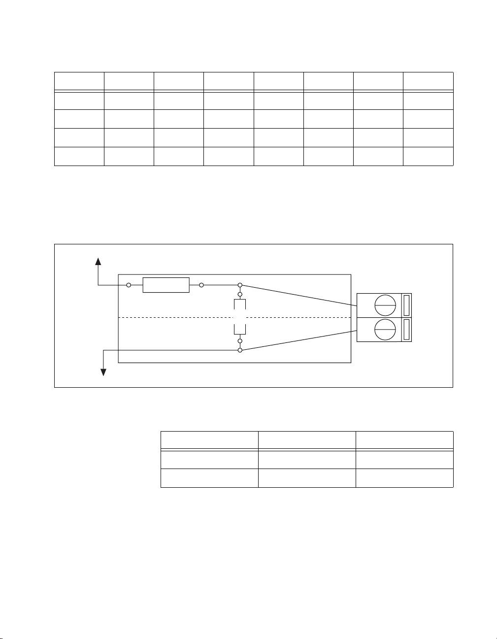
Chapter 5 Adding Components for Special Functions
Table 5-1. Component Location for Analog Input Channels in DIFF Input Mode (Continued)
Channel A B C D E F G
ACH4 R30 RC20 RC21 R31 RC8 R12 R13
ACH5 R32 RC22 RC23 R33 RC9 R14 R15
ACH6 R34 RC24 RC25 R35 RC10 R16 R17
ACH7 R36 RC26 RC27 R37 RC11 R18 R19
Conditioning Analog Output Channels
Figure 5-2 illustrates the generic AO channel pad configuration, and
Table 5-2 describes the AO component locations and labels. Figure 5-3
shows the AO channel configuration for DAC0OUT.
DACOUT
(A)
AOGND
(B)
Figure 5-2. Analog Output Channel Configuration Diagram
Table 5-2. Component Location for Analog Output Channels in DIFF Input Mode
Channel A B
DAC0OUT R3 RC3
DAC1OUT R2 RC2
© National Instruments Corporation 5-3 SCB-68 Shielded Connector Block User Manual
Page 49

Chapter 5 Adding Components for Special Functions
Figure 5-3. Analog Output Channel Configuration Diagram for DAC0OUT
Conditioning PFI0/TRIG1
Figure 5-4 illustrates the digital input channel configuration, and
Figure 5-5 shows the digital input channel configuration for PFI0/TRIG1.
PFI0/TRIG1
DAC0OUT
AOGND
(RC1)
(R1)
R3
+
RC3
C
–
11
44
DGND
Figure 5-4. Digital Input Channel Configuration Diagram
PFI0/TRIG1
RC1
DGND
Figure 5-5. Digital Input Channel Configuration Diagram for PFI0/TRIG1
SCB-68 Shielded Connector Block User Manual 5-4 ni.com
R0
+
C
–
Page 50

Chapter 5 Adding Components for Special Functions
Accuracy and Resolution Considerations
When you measure voltage to subsequently measure current, take the
following steps to maximize measurement accuracy:
1. Refer to the accuracy tables in Appendix A, Specifications, of the DAQ
device user manual at
2. Use Equation 5-1 to determine the code width, which is the smallest
signal change that a system can detect.
3. Divide code width by the resistor value to determine the minimum
current value you can measure.
ni.com/manuals.
Code Width
In Equation 5-1, range defines the values between and including the
minimum and maximum voltages that the ADC can digitize. For example,
the range is 20 when you measure a signal between –10 to 10 V. Gain,
which is determined by the input limits of the application, is a value you
apply to amplify or attenuate the signal.
Gain is expressed in decibels and is defined as:
Gain 20 Log f()=
Resolution, or the smallest signal increment that can be detected by a
measurement system, is either 12 or 16 bits, depending on the DAQ device.
Open Thermocouple Detection
As an option, you can build open thermocouple detection circuitry by
connecting a high-value resistor between the positive input and +5V.
A resistor of a few MΩ or more is sufficient, but a high-value resistor
allows you to detect an open or defective thermocouple. If the
thermocouple opens, the voltage measured across the input terminals rises
to +5 V, a value much larger than any legitimate thermocouple voltage.
You can create a bias current return path by using a 100 kΩ resistor
between the negative input and AIGND.
Range
-------------------------------------------=
Gain 2
×
Resolution
(5-1)
(5-2)
© National Instruments Corporation 5-5 SCB-68 Shielded Connector Block User Manual
Page 51

Chapter 5 Adding Components for Special Functions
Differential Open Thermocouple Detection
Use position A to connect a high-value resistor between the positive input
and +5V. Leave the jumpers in place (positions F and G) for each channel
used.
Single-Ended Open Thermocouple Detection
Use position A for one channel and C for the next channel when you
connect a high-value resistor between the positive input and +5V. Leave
the jumpers at positions F and G in place for each channel used.
Sources of Error
When making thermocouple measurements with the SCB-68, the possible
sources of error are compensation, linearization, measurement, and
thermocouple wire errors.
Compensation error can arise from two sources—inaccuracy of the
temperature sensor and temperature differences between the temperature
sensor and the screw terminals. The temperature sensor on the SCB-68 is
specified to be accurate to ±1 °C. You can minimize temperature
differences between the temperature sensor and the screw terminals by
keeping the SCB-68 away from drafts, heaters, and warm equipment.
Thermocouple output voltages are nonlinear with respect to temperature.
Conversion of the voltage output to temperature using either look-up tables
or polynomial approximations introduces linearization error. The
linearization error is dependent upon how closely the table or the
polynomial approximates the true thermocouple output. For example, you
can reduce the linearization error by using a higher degree polynomial.
Measurement error is the result of inaccuracies in the DAQ device. These
inaccuracies include gain and offset. If the device is properly calibrated, the
offset error should be zeroed out. The only remaining error is a gain error
of ±0.08% of full range. If the input range is ±10 V and the gain is 500, gain
error contributes 0.0008 × 20 mV, or 16 µV of error. If the Seebeck
coefficient of a thermocouple is 32 µV/°C, this measurement error adds
0.5 °C of uncertainty to the measurement. For best results, you must use a
well-calibrated DAQ device so that offsets can be ignored. You can
eliminate offset error, however, by grounding one channel on the SCB-68
and measuring the voltage. You can then subtract this value, the offset of
the DAQ device, in software from all other readings.
SCB-68 Shielded Connector Block User Manual 5-6 ni.com
Page 52

Thermocouple wire error is the result of inconsistencies in the
thermocouple manufacturing process. These inconsistencies, or
nonhomogeneities, are the result of defects or impurities in the
thermocouple wire. The errors vary widely depending upon the
thermocouple type and even the gauge of wire used, but an error of ±2 °C
is typical. For more information on thermocouple wire errors and more
specific data, consult the thermocouple manufacturer.
For best results, use the average of many readings (about 100 or so); typical
absolute accuracies should then be about ±2 °C.
Lowpass Filtering
This section discusses lowpass filtering and how to add components for
lowpass filtering.
Theory of Operation
Lowpass filters highly or completely attenuate signals with frequencies
above the cut-off frequency, or high-frequency stopband signals, but
lowpass filters do not attenuate signals with frequencies below the cut-off
frequency, or low-frequency passband signals. Ideally, lowpass filters have
a phase shift that is linear with respect to frequency. This linear phase shift
delays signal components of all frequencies by a constant time,
independent of frequency, thereby preserving the overall shape of the
signal.
Chapter 5 Adding Components for Special Functions
In practice, lowpass filters subject input signals to a mathematical transfer
function that approximates the characteristics of an ideal filter. By
analyzing the Bode Plot, or the plot that represents the transfer function,
you can determine the filter characteristics.
Figures 5-6 and 5-7 show the Bode Plots for the ideal filter and the real
filter, respectively, and indicate the attenuation of each transfer function.
© National Instruments Corporation 5-7 SCB-68 Shielded Connector Block User Manual
Page 53

Chapter 5 Adding Components for Special Functions
Figure 5-6. Transfer Function Attenuation for an Ideal Filter
Gain
Passband
Stopband
f
c
Log Frequency
Gain
Passband
Transition
Region
f
c
Stopband
Log Frequency
Figure 5-7. Transfer Function Attenuation for a Real Filter
The cut-off frequency, fc, is defined as the frequency beyond which the gain
drops 3 dB. Figure 5-6 shows how an ideal filter causes the gain to drop to
zero for all frequencies greater than f
. Thus, fc does not pass through the
c
filter to its output. Instead of having a gain of absolute zero for frequencies
greater than f
, the real filter has a transition region between the passband
c
and the stopband, a ripple in the passband, and a stopband with a finite
attenuation gain.
Real filters have some nonlinearity in their phase response, causing signals
at higher frequencies to be delayed by longer times than signals at lower
frequencies and resulting in an overall shape distortion of the signal.
For example, when the square wave shown in Figure 5-8 enters a filter, an
ideal filter smooths the edges of the input, whereas a real filter causes some
SCB-68 Shielded Connector Block User Manual 5-8 ni.com
Page 54

Chapter 5 Adding Components for Special Functions
ringing in the signal as the higher frequency components of the signal are
delayed.
Volts (V)
Time (t)
Figure 5-8. Square Wave Input Signal
Figures 5-9 and 5-10 show the difference in response to a square wave
between an ideal and a real filter, respectively.
Volts (V)
Time (t)
Figure 5-9. Response of an Ideal Filter to a Square Wave Input Signal
© National Instruments Corporation 5-9 SCB-68 Shielded Connector Block User Manual
Page 55

Chapter 5 Adding Components for Special Functions
Figure 5-10. Response of a Real Filter to a Square Wave Input Signal
One-Pole Lowpass RC Filter
Figure 5-11 shows the transfer function of a simple series circuit consisting
of a resistor (R) and capacitor (C) when the voltage across R is assumed to
be the output voltage (V
Volts (V)
).
m
Time (t)
C
in
RV
V
m
Figure 5-11. Transfer Function of a Simple Series Circuit
The transfer function is a mathematical representation of a one-pole
lowpass filter, with a time constant of
1
--------------2π RC
as follows:
Ts()
SCB-68 Shielded Connector Block User Manual 5-10 ni.com
-------------------------------=
12πRC()s+
G
(5-3)
Page 56

Use Equation 5-3 to design a lowpass filter for a simple resistor and
capacitor circuit, where the values of the resistor and capacitor alone
determine f
frequency domain.
Selecting Components
To determine the value of the components in the circuit, fix R (10 kΩ is
reasonable) and isolate C from Equation 5-3 as follows:
Chapter 5 Adding Components for Special Functions
. In this equation, G is the DC gain and s represents the
c
Adding Components
C
The cut-off frequency in Equation 5-4 is f
1
---------------=
2π Rf
(5-4)
c
.
c
For best results, choose a resistor that has the following characteristics:
• Low wattage of approximately 1/8 W
• Precision of at least 5%
• Temperature stability
• Tolerance of 5%
• AXL package (suggested)
• Carbon or metal film (suggested)
Choose a capacitor that has the following suggested characteristics:
• AXL or RDL package
• Tolerance of 20%
• Maximum voltage of at least 25 V
Using the circuit shown in Figure 5-11, you can use a two-component
circuit to build a simple RC filter with analog input, analog output, or
digital input. You can build a single-ended analog input RC filter with pads
F and B for one channel and pads G and D for the next channel. You can
build a differential analog input RC filter with pads F and E.
For TRIG1, you can use pads R1 and RC1. For AO, you can use R2 and
RC2 for DAC1OUT, and you can use R3 and RC3 for DAC0OUT.
© National Instruments Corporation 5-11 SCB-68 Shielded Connector Block User Manual
Page 57

Chapter 5 Adding Components for Special Functions
f
For any type of lowpass filter, use Equation 5-5 to determine the cut-off
frequency (f
).
c
Single-Ended Lowpass Filter
To build a single-ended lowpass filter, refer to Figure 5-12. Add the resistor
to position B or D, depending on the AI channel you are using. Add the
capacitor to position F or G, depending on the AI channel you are using.
Figure 5-12. SCB-68 Circuit Diagram for a Single-Ended Lowpass Filter
ACH<i>
+
V
in
–
AIGND
1
c
---------------=
2π RC
(5-5)
C
F,G
R
B,D
+
V
m
–
Differential Lowpass Filter
To build a differential lowpass filter, refer to Figure 5-13. Add the resistor
to position E and the capacitor to position F.
C
i
+8>
F
R
E
+
V
m
–
ACH<i>
+
V
in
–
ACH<
Figure 5-13. SCB-68 Circuit Diagram for a Differential Lowpass Filter
Analog Output and Digital Input Lowpass Filtering
For DAC0OUT, add the resistor to position RC3 and the capacitor to
position R3. For DAC1OUT, add the resistor to position RC2 and the
capacitor to position R2.
For TRIG1, add the resistor to position RC1 and the capacitor to
position R1.
SCB-68 Shielded Connector Block User Manual 5-12 ni.com
Page 58
Lowpass Filtering Applications
Noise filtering and antialiasing are two applications that use lowpass filters.
Noise Filtering
You can use a lowpass filter to highly attenuate the noise frequency on a
measured signal. For example, power lines commonly add a noise
frequency of 60 Hz. Adding a filter with f
measurement system causes the noise frequency to fall into the stopband.
Referring to Equation 5-4, fix the resistor value at 10 kΩ to calculate the
capacitor value and choose a commercial capacitor value that satisfies the
following relationship:
Chapter 5 Adding Components for Special Functions
< 60 Hz at the input of the
c
-----------------------------------------
C
>
2π 10 000,()60()
1
(5-6)
Antialiasing Filtering
Aliasing causes high-frequency signal components to appear as a
low-frequency signal, as Figure 5-14 shows.
1
–1
2468100
Input Signal
Sampled Points
Reconstructed Signal
Figure 5-14. Aliasing of a High-Frequency Signal
The solid line depicts a high-frequency signal being sampled at the
indicated points. When these points are connected to reconstruct the
waveform, as shown by the dotted line, the signal appears to have a lower
frequency. Any signal with a frequency greater than one-half of its sample
rate is aliased and incorrectly analyzed as having a frequency below
one-half the sample rate. This limiting frequency of one-half the sample
rate is known as the Nyquist frequency.
© National Instruments Corporation 5-13 SCB-68 Shielded Connector Block User Manual
Page 59

Chapter 5 Adding Components for Special Functions
To prevent aliasing, remove all signal components with frequencies greater
than the Nyquist frequency from input signals before those signals are
sampled. Once a data sample is aliased, it is impossible to accurately
reconstruct the original signal.
To design a lowpass filter that attenuates signal components with a
frequency higher than half of the Nyquist frequency, substitute the half
Nyquist value for the f
The following devices provide antialiasing filters and do not need to have
the filters implemented at the SCB-68 terminal block:
• NI PCI/PXI-61XX (not including the NI PCI-6110/6111)
• NI PCI-445X
• NI PCI-455X
value in Equation 5-6.
c
Special Consideration for Analog Input Channels
Filtering increases the settling time of the instrumentation amplifier to the
time constant of the filter used. Adding RC filters to scanning channels
greatly reduces the practical scanning rate, since the instrumentation
amplifier settling time can be increased to 10T or longer, where T =(R)(C).
You can use RC filters with single-ended or differential inputs.
Special Consideration for Analog Output Signals
Lowpass filters can smooth stairstep-like curves on AO signals. If the
curves are not smoothed, the AO signals can be a hazard for some external
circuitry connected to it. Figure 5-15 shows the output of a lowpass filter
when a stairstep-like signal is the input.
SCB-68 Shielded Connector Block User Manual 5-14 ni.com
Page 60

Chapter 5 Adding Components for Special Functions
Volts (V)
Time (t)
Figure 5-15. Lowpass Filtering of AO Signals
Special Consideration for Digital Trigger Input Signals
Lowpass filters can function as debouncing filters to smooth noise on
digital trigger input signals, thus enabling the trigger-detection circuitry of
the DAQ device to understand the signal as a valid digital trigger.
TTL Logic
High
TTL Logic
Volts (V)
Low
Time (t)
Figure 5-16. Digital Trigger Input Signal with a High-Frequency Component
© National Instruments Corporation 5-15 SCB-68 Shielded Connector Block User Manual
Page 61

Chapter 5 Adding Components for Special Functions
Apply a lowpass filter to the signal to remove the high-frequency
component for a cleaner digital signal, as Figure 5-17 shows.
Figure 5-17. Lowpass Filtering of Digital Trigger Input Signals
Note
Due to the filter order, the digital trigger input signal is delayed for a specific amount
of time before the DAQ device senses the signal at the trigger input.
Volts (V)
Time (t)
Measuring a 4 to 20 mA Current
Since DAQ devices cannot directly measure current, this section describes
how to add components for measuring current when transistors output a
current value ranging between 4 and 20 mA.
Theory of Operation
The conversion from current to voltage is based on Ohm’s Law, which is
summarized by Equation 5-7, where V is voltage, I is current and R is
resistance:
VIR×=
Thus, you must multiply current by a constant to convert the current to a
voltage. In an electrical circuit, current must flow through a resistor to
produce a voltage drop. This voltage drop then becomes the input for a
DAQ device, as Figure 5-18 shows.
SCB-68 Shielded Connector Block User Manual 5-16 ni.com
(5-7)
Page 62
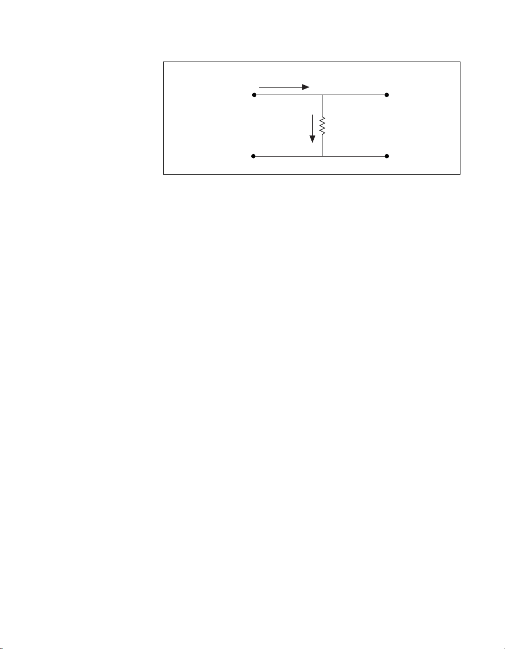
Chapter 5 Adding Components for Special Functions
I
+
+
Selecting a Resistor
Transducer
Input
–
Figure 5-18. Current-to-Voltage Electrical Circuit
R
V
m
–
The application software must linearly convert voltage back to current.
Equation 5-8 demonstrates this conversion, where the resistor is the
denominator and V
is the input voltage into the DAQ device:
in
V
m
------=
I
R
(5-8)
For best results when measuring current, you should choose a resistor that
has the following characteristics:
• Low wattage of approximately 1/8 W
• Precision of at least 5%
• Temperature stability
• Tolerance of 5%
• 232 Ω (suggested)
• AXL package (suggested)
• Carbon or metal film (suggested)
If you use the resistor described above, you can convert a 20 mA current to
4.64 V by setting the device range to either (–5 to +5 V) or (0 to 5 V).
© National Instruments Corporation 5-17 SCB-68 Shielded Connector Block User Manual
Page 63

Chapter 5 Adding Components for Special Functions
Adding Components
Caution Do not exceed ±10 V at the analog inputs. NI is not liable for any device damage
or personal injury resulting from improper connections.
You can build a one-resistor circuit for measuring current at the
single-ended or differential inputs of the SCB-68.
Single-Ended Inputs
To build a one-resistor circuit that measures current at the single-ended
analog inputs of the SCB-68, add the resistor to position B or D depending
on the channel being used. Leave the jumpers in place for channel positions
F and G, respectively. Calculate the current according to Equation 5-9
or 5-10.
V
m
I
------=
R
B
V
m
I
------=
R
E
(5-9)
(5-10)
Differential Inputs
To build a one-resistor circuit that measures current at the differential
inputs of the SCB-68, add the resistor to position E for each differential
channel pair that is used. Leave the jumpers in place for positions F and G.
Calculate the current according to Equation 5-11:
V
m
------=
I
R
E
(5-11)
Attenuating Voltage
This section describes how to add components for attenuating, or
decreasing the amplitude of, a voltage signal. Transducers can output more
than 10 V
per input channel. Therefore, you must attenuate output signals from the
transducer to fit within the DAQ device specifications. Figure 5-19 shows
how to use a voltage divider to attenuate the output signal of the transducer.
SCB-68 Shielded Connector Block User Manual 5-18 ni.com
per channel, but DAQ devices cannot read more than 10 VDC
DC
Page 64

Chapter 5 Adding Components for Special Functions
R
+
1
+
Theory of Operation
V
in
–
R
2
V
m
–
Figure 5-19. Attenuating Voltage with a Voltage Divider
The voltage divider splits the input voltage (Vin) between two resistors
(R
and R2), causing the voltage on each resistor to be noticeably lower than
1
V
. Use Equation 5-12 to determine the Vm that the DAQ device measures:
in
R
2
V
m
------------------
V
=
in
R1R2+
(5-12)
Use Equation 5-13 to determine the overall gain of a voltage divider circuit:
V
m
-------
G
V
in
R
------------------==
R1R2+
2
(5-13)
The accuracy of Equation 5-13 depends on the tolerances of the resistors
that you use.
Caution The SCB-68 is not designed for any input voltages greater than 42 V, even if a
user-installed voltage divider reduces the voltage to within the input range of the DAQ
device. Input voltages greater than 42 V can damage the SCB-68, any devices connected
to it, and the host computer. Overvoltage can also cause an electric shock hazard for the
operator. NI is not responsible for damage or injury resulting from such misuse.
© National Instruments Corporation 5-19 SCB-68 Shielded Connector Block User Manual
Page 65

Chapter 5 Adding Components for Special Functions
Selecting Components
To set up the resistors, complete the following steps:
1. Select the value for R
2. Use Equation 5-12 to calculate the value for R
on the following values:
• Maximum V
• Maximum voltage (<10 V
device
Accuracy Considerations
For best results when attenuating voltage, you should choose a resistor that
has the following characteristics:
• Low wattage of approximately 1/8 W
• Precision of at least 5%
• Temperature stable
• Tolerance of 5%
• AXL package (suggested)
• Carbon or metal film (suggested)
(10 kΩ is recommended).
2
. Base the R1 calculation
1
you expect from the transducer
in
) that you want to input to the DAQ
DC
Ver if y t h a t R
and R2 drift together with respect to temperature; otherwise,
1
the system may consistently read incorrect values.
Adding Components
You an build a two- or three-resistor circuit for attenuating voltages at the
single-ended inputs, differential inputs, analog outputs, and digital inputs
of the SCB-68.
Single-Ended Input Attenuators
To build a two-resistor circuit for attenuating voltages at the single-ended
inputs of the SCB-68, refer to Figure 5-20.
SCB-68 Shielded Connector Block User Manual 5-20 ni.com
Page 66

Chapter 5 Adding Components for Special Functions
ACH<i>
+
V
–
AIGND
R
F,G
R
in
B,D
+
V
m
–
Figure 5-20. SCB-68 Circuit Diagram for SE Input Attenuation
Install resistors in positions B and F, or positions D and G, depending on
the channel you are using on the SCB-68. Use Equations 5-14 or 5-15 to
calculate the gain of the circuit:
G
------------------------=
RBRF+()
G
R
-------------------------=
RDRG+()
B
D
(5-14)
(5-15)
R
Differential Input Attenuators
To build a three-resistor circuit for attenuating voltages at the differential
inputs of the SCB-68, refer to Figure 5-21.
i
+8>
R
F
R
E
R
G
+
V
m
–
ACH<i>
+
V
in
–
ACH<
Figure 5-21. SCB-68 Circuit Diagram for DIFF Input Attenuation
Install resistors in positions E, F, and G of the chosen differential channel
pair. Use Equation 5-16 to determine the gain of the circuit:
R
-------------------------------------=
G
© National Instruments Corporation 5-21 SCB-68 Shielded Connector Block User Manual
E
RERFR
++()
G
(5-16)
Page 67

Chapter 5 Adding Components for Special Functions
Analog Output and Digital Input Attenuators
To build a two-resistor circuit for attenuating voltages at the DAC0OUT,
DAC1OUT, and TRIG1 pins on the SCB-68, refer to the pad positions in
Figure 5-22.
Figure 5-22. SCB-68 Circuit Diagram for Digital Input Attenuation
Use positions R1 and RC1 for TRIG1, and determine the gain according to
Equation 5-17:
ACH<i>
+
V
in
–
ACH<
i
+8>
C
F
R
E
+
V
m
–
G
Use positions R2 and RC2 for DAC1OUT, and determine the gain
according to Equation 5-18:
G
Use positions R3 and RC3 for DAC0OUT, and determine the gain
according to Equation 5-19:
G
Special Considerations for Analog Input
When calculating the values for R1 and R2, consider the input impedance
value from the point of view of V
RC1
-----------------------------=
RC1 R1+()
RC2
-----------------------------=
RC2 R2+()
RC3
-----------------------------=
RC3 R3+()
, as Figure 5-23 shows.
in
(5-17)
(5-18)
(5-19)
SCB-68 Shielded Connector Block User Manual 5-22 ni.com
Page 68

Chapter 5 Adding Components for Special Functions
R
+
1
+
V
in
–
Figure 5-23. Input Impedance Electrical Circuit
Zin is the new input impedance. Refer to Appendix A, Specifications, in the
device user manuals at
ni.com/manuals for the input impedance.
Equation 5-20 shows the relationship among all of the resistor values:
Z
in
R2Input Impedance×()
R
---------------------------------------------------------+=
1
R
Special Considerations for Analog Output
When you use the circuit shown in Figure 5-19 for AO, the output
impedance changes. Thus, you must choose the values for R
the final output impedance value is as low as possible. Refer to
Appendix A, Specifications, in the device user manuals at
ni.com/manuals for device specifications. Figure 5-24 shows the
electrical circuit you use to calculate the output impedance.
R
1
R
2
Input Impedance+()
2
Input
Impedance
–
and R2 so that
1
Z
out
(5-20)
Output
Impedance
R
2
Figure 5-24. Electrical Circuit for Determining Output Impedance
Equation 5-21 shows the relationship between R1, R2, and Z
is the old output impedance and Z
Z
out2
© National Instruments Corporation 5-23 SCB-68 Shielded Connector Block User Manual
is the new output impedance:
out2
Z
+()R2×
outR1
---------------------------------------=
++
Z
outR1R2
, where Z
out
out
(5-21)
Page 69

Chapter 5 Adding Components for Special Functions
Special Considerations for Digital Inputs
If you use the Vin voltage of Figure 5-20 to feed TTL signals, you must
calculate V
so that the voltage drop on R2 does not exceed 5 V.
in
Caution A voltage drop exceeding 5 V on R
can damage the internal circuitry of the DAQ
2
device. NI is not liable for any device damage or personal injury resulting from improper
use of the SCB-68 and the DAQ device.
SCB-68 Shielded Connector Block User Manual 5-24 ni.com
Page 70

Specifications
This appendix lists the SCB-68 specifications. These ratings are typical at
25 °C unless otherwise stated.
Analog Input
Number of channels
68-pin DAQ devices ....................... Eight differential,
100-pin DAQ devices ..................... 32 differential,
Temperature sensor
Accuracy ......................................... ±1.0 °C over a 0 to 110 °C range
Output .............................................10 mV/°C
Power Requirement
Power consumption (at +5 VDC, ±5%)
Typical ............................................ 1 mA with no signal
Maximum........................................ 800 mA from host computer
A
16 single-ended
64 single-ended
conditioning installed
Note The power specifications pertain to the power supply of the host computer when
using internal power or to the external supply connected at the +5 V screw terminal when
using external power. The maximum power consumption of the SCB-68 is a function
of the signal conditioning components installed and any circuits constructed on the
general-purpose breadboard area. If the SCB-68 is powered from the host computer,
the maximum +5 V current draw, which is limited by the fuse, is 800 mA.
Fuse
Manufacturer.......................................... Littelfuse
Part number ............................................ 235 800
Ampere rating ........................................ 0.800 A
© National Instruments Corporation A-1 SCB-68 Shielded Connector Block User Manual
Page 71

Chapter A Specifications
Voltage rating .........................................250 V
Nominal resistance .................................0.195 Ω
Physical
Box dimensions (including box feet)......19.5 by 15.2 by 4.5 cm
I/O connectors.........................................One 68-pin male SCSI connector
Screw terminals ......................................68
Wire gauge..............................................≤26 AWG
Resistor sockets ......................................0.032 to 0.038 in. (in diameter)
Maximum Working Voltage
Maximum working voltage refers to the signal voltage plus the
common-mode voltage.
(7.7 by 6.0 by 1.8 in.)
Environmental
Channel-to-earth .....................................42 V
Channel-to-channel.................................42 V
Operating temperature ............................0 to 70 °C
Storage temperature ................................–20 to 70 °C
Humidity.................................................5 to 90% RH, noncondensing
Maximum altitude...................................2000 meters
Pollution Degree (indoor use only) ........II
, Installation Category II
rms
, Installation Category II
rms
SCB-68 Shielded Connector Block User Manual A-2 ni.com
Page 72

Safety
The SCB-68 meets the requirements of the following standards for safety
and electrical equipment for measurement, control, and laboratory use:
• IEC 61010-1, EN 61010-1
• UL 3111-1
• CAN/CSA C22.2 No. 1010.1
Note For UL and other safety certifications, refer to the product label or to ni.com.
Electromagnetic Compatibility
Emissions ............................................... EN 55011 Class A at 10 m
Immunity................................................ EN 61326-1:1997 + A1:1998,
EMC/EMI............................................... CE, C-Tick, and FCC Part 15
Note For EMC compliance, you must operate this device with shielded cabling.
Chapter A Specifications
FCC Part 15A above 1 GHz
Table 1
(Class A) Compliant
CE Compliance
This product meets the essential requirements of applicable European
Directives, as amended for CE Marking, as follows:
Low-Voltage Directive (safety) ............. 73/23/EEC
Electromagnetic Compatibility
Directive (EMC) .................................... 89/336/EEC
Note Refer to the Declaration of Conformity (DoC) for this product for any additional
regulatory compliance information. To obtain the DoC for this product, click Declaration
of Conformity at
family. Select the appropriate product family, followed by your product, and a link to
the DoC appears in Adobe Acrobat format. Click the Acrobat icon to download or read
the DoC.
© National Instruments Corporation A-3 SCB-68 Shielded Connector Block User Manual
ni.com/hardref.nsf/. This Web site lists the DoCs by product
Page 73

Quick Reference Labels
This appendix shows the pinouts that appear on the quick reference labels
for the DAQ devices that are compatible with the SCB-68.
B
© National Instruments Corporation B-1 SCB-68 Shielded Connector Block User Manual
Page 74
Chapter B Quick Reference Labels
SCB-68 Quick Reference Label
NATIONAL
INSTRUMENTS
P/N 182509B-01
FACTORY DEFAULT SETTING
0
S4
S5
* TEMP. SENSOR DISABLED
* ACCESSORY POWER ON
S4
S5
* TEMP. SENSOR ENABLED
ON SINGLE ENDED CH. 0
* ACCESSORY POWER ON
S4
S5
* TEMP. SENSOR ENABLED
ON DIFFERENTIAL CH. 0
* ACCESSORY POWER ON
S4
S5
* 68 GENERIC TERMINALS
(TEMP. SENSOR AND
ACCESSORY POWER OFF)
S1
S2
S3
S1
S2
S3
S1
S2
S3
S1
S2
S3
E SERIES DEVICES
PIN # SIGNAL
68
ACH0
34
ACH8
67
AIGND
33
ACH1
66
ACH9
32
AIGND
65
ACH2
31
ACH10
64
AIGND
30
ACH3
63
ACH11
29
AIGND
62
AISENSE
28
ACH4
61
ACH12
27
AIGND
60
ACH5
26
ACH13
59
AIGND
25
ACH6
58
ACH14
24
AIGND
57
ACH7
ACH15
23
12
46
13
47
14
48
15
49
16
50
17
51
18
52
19
53
20
54
21
55
22
56
DGND
SCANCLK
DGND
DIO3
+5V
DIO7
DGND
DIO2
DIO6
DGND
DIO1
DIO5
DGND
DIO0
DIO4
DGND
EXTREF
AOGND
DAC1 OUT
AOGND
DAC0 OUT
AIGND
37
10
1
35
2
GPCTR0_OUT
36
PFI9/GPCTR0_GATE
3
PFI8/GPCTR0_SOURCE
4
38
5
PFI7/STARTSCAN
PFI6/WFTRIG
39
6
40
PFI5/UPDATE*
GPCTR1_OUT
7
PFI4/GPCTR1_GATE
41
8
42
PFI3/GPCTR1_SOURCE
9
43
PFI2/CONVERT*
44
11
45
EXTSTROBE*
SIGNALPIN #PIN # SIGNAL
FREQ_OUT
DGND
DGND
DGND
DGND
DGND
+5V, FUSED
DGND
PFI1/TRIG2
DGND
PFI0/TRIG1
Figure B-1. E Series Devices
SCB-68 Shielded Connector Block User Manual B-2 ni.com
Page 75
Chapter B Quick Reference Labels
SCB-68 Quick Reference Label
NATIONAL
INSTRUMENTS
*NO CONNECT ON THE NI 6703
S1
S4
S5
* 68 GENERIC TERMINALS
(TEMP. SENSOR AND
ACCESSORY POWER OFF)
S2
S3
NI 670X DEVICES
PIN # SIGNAL
68
AGND0/AGND16
34
VCH0
67
ICH16*
33
AGND1/AGND17
66
VCH1
32
ICH17*
65
AGND2/AGND18
31
VCH2
64
ICH18*
30
AGND3/AGND19
63
VCH3
29
ICH19*
62
AGND4/AGND20
28
VCH4
61
ICH20*
27
AGND5/AGND21
60
VCH5
26
ICH21*
59
AGND6/AGND22
25
VCH6
58
ICH22*
24
AGND7/AGND23
57
VCH7
23
ICH23*
PIN # SIGNAL
12
VCH14
46
AGND14/AGND30
13
ICH29*
VCH13
47
AGND13AGND29
14
ICH28*
48
15
VCH12
AGND12/AGND28
49
ICH27*
16
50
AGND11/AGND27
VCH11
17
ICH26*
51
18
AGND10/AGND26
VCH10
52
AGND
19
53
ICH25*
20
AGND9/AGND25
54
VCH9
21
ICH24*
55
AGND8/AGND24
22
VCH8
AGND
56
1
35
2
36
3
37
4
38
5
39
6
40
7
41
8
42
9
43
10
44
11
45
SIGNALPIN #
+5V OUTPUT
DGND
DIO0
DGND
DIO1
DGND
DIO2
RFU
DIO3
DGND
DIO4
DGND
DIO5
DGND
DIO6
DGND
DIO7
AGND
ICH31*
VCH15
AGND15/AGND31
ICH30*
Figure B-2. NI 670X Devices
© National Instruments Corporation B-3 SCB-68 Shielded Connector Block User Manual
Page 76

Chapter B Quick Reference Labels
SCB-68 Quick Reference Label
NATIONAL
INSTRUMENTS
FACTORY DEFAULT SETTING
S1
S4
S5
* TEMP. SENSOR DISABLED
* ACCESSORY POWER ON
S4
S5
* 68 GENERIC TERMINALS
(TEMP. SENSOR AND
ACCESSORY POWER OFF)
S2
S3
S1
S2
S3
NI 671X/673X DEVICES
PIN # SIGNAL
68
NC
34
AOGND
67
33
66
32
65
31
64
30
63
29
62
28
61
27
60
26
59
25
58
24
57
23
AOGND
NC
AOGND
AOGND
DAC7OUT
AOGND
AOGND
DAC6OUT
AOGND
AOGND
NC
DAC5OUT
AOGND
AOGND
DAC4OUT
AOGND
AOGND
DAC3OUT
AOGND
AOGND
DAC2OUT
AOGND
12
46
13
47
14
48
15
49
16
50
17
51
18
52
19
53
20
54
21
55
22
56
DGND
NCC
DGND
DIO3
+5V
DIO7
DGND
DIO2
DIO6
DGND
DIO1
DIO5
DGND
DIO0
DIO4
DGND
EXTREF
AOGND
DAC1 OUT
AOGND
DAC0 OUT
AIGND
37
10
1
35
2
GPCTR0_OUT
36
PFI9/GPCTR0_GATE
3
PFI8/GPCTR0_SOURCE
4
38
5
PFI6/WFTRIG
39
6
40
PFI5/UPDATE*
GPCTR1_OUT
7
PFI4/GPCTR1_GATE
41
8
42
PFI3/GPCTR1_SOURCE
9
43
44
11
45
EXTSTROBE*
SIGNALPIN #PIN # SIGNAL
FREQ_OUT
DGND
DGND
DGND
PFI7
DGND
DGND
+5V, FUSED
DGND
PFI2
PFI1
DGND
PFI0
Figure B-3. NI 671X/673X Devices
SCB-68 Shielded Connector Block User Manual B-4 ni.com
Page 77
Chapter B Quick Reference Labels
SCB-68 Quick Reference Label
NATIONAL
INSTRUMENTS
P/N 182509B-01
FACTORY DEFAULT SETTING
S1
S4
S5
* TEMP. SENSOR DISABLED
* ACCESSORY POWER ON
S4
S5
* TEMP. SENSOR ENABLED
ON DIFFERENTIAL CH. 0
* ACCESSORY POWER ON
S4
S5
* 68 GENERIC TERMINALS
(TEMP. SENSOR AND
ACCESSORY POWER OFF)
S2
S3
S1
S2
S3
S1
S2
S3
S SERIES DEVICES
PIN # SIGNAL
68
ACH0
34
ACH0-
67
33
66
32
65
31
64
30
63
29
62
28
61
27
60
26
59
25
58
24
57
23
ACH0GND
ACH1+
ACH1-
ACH1GND
ACH2+
ACH2-
ACH2GND
ACH3+
ACH3-
ACH3GND
NC
NC
NC
NC
NC
NC
NC
NC
NC
NC
NC
NC
12
46
13
47
14
48
15
49
16
50
17
51
18
52
19
53
20
54
21
55
22
56
DGND
SCANCLK
DGND
DIO3
+5V
DIO7
DGND
DIO2
DIO6
DGND
DIO1
DIO5
DGND
DIO0
DIO4
DGND
NC
AOGND
DAC1OUT
AOGND
DAC0OUT
NC
37
10
35
36
38
39
40
41
42
43
44
11
45
1
2
3
FREQ_OUT
GPCTR0_OUT
PFI9/GPCTR0_GATE
PFI8/GPCTR0_SOURCE
4
PFI7/STARTSCAN
5
6
PFI6/WFTRIG
PFI5/UPDATE*
GPCTR1_OUT
7
PFI4/GPCTR1_GATE
8
+5V, FUSED
PFI3/GPCTR1_SOURCE
9
PFI2/CONVERT*
PFI1/TRIG2
PFI0/TRIG1
EXTSTROBE*
SIGNALPIN #PIN # SIGNAL
DGND
DGND
DGND
DGND
DGND
DGND
DGND
Figure B-4. S Series Devices
© National Instruments Corporation B-5 SCB-68 Shielded Connector Block User Manual
Page 78
Chapter B Quick Reference Labels
SCB-68 Quick Reference Label
NATIONAL
INSTRUMENTS
NI 660X DEVICES
If using an NI 660X device
with an optional SCB-68
shielded connector block
accessory, affix this label
to the inside of the SCB-68
and set the switches as
shown below.
P/N 185974A-01
SET SWITCHES AS
FOLLOWS FOR
NI 660
X
DEVICES.
S1
S2
S5
S4
S3
Application Contexts:
Counter
As shown on label
DIO (n= 0..31)
DIO_0 maps to PFI_0
DIO_n maps to PFI_n
Motion Encoder (n= 0..7)
SOURCE_n maps to CH_A_n
UP_DOWN_n maps to CH_B_n
GATE_n maps to CH_Z_n
For details, refer to
ni.com/manuals
manual for NI 660
for the user
X
devices.
PIN#
68
34
67
33
66
32
65
31
64
30
63
29
62
28
61
27
60
26
59
25
58
24
57
23
SIGNAL
GND
PFI_31 (SOURCE_2)
PFI_30 (GATE_2)
GND
PFI_29 (UP_DOWN_2)
PFI_28 (OUT_2)
GND
PFI_27 (SOURCE_3)
PFI_26 (GATE_3)
GND
PFI_25 (UP_DOWN_3)
PFI_24 (OUT_3)
GND
PFI_23 (SOURCE_4)
PFI_22 (GATE_4)
GND
PFI_21 (UP_DOWN_4)
PFI_20 (OUT_4)
GND
PFI_19 (SOURCE_5)
PFI_18 (GATE_5)
GND
PFI_17 (UP_DOWN_5)
PFI_16 (OUT_5)
PIN#
12
46
13
47
14
48
15
49
16
50
17
51
18
52
19
53
20
54
21
55
22
56
SIGNAL
PFI_3
GND
PFI_4
PFI_5
GND
PFI_6
PFI_7
GND
PFI_8 (OUT_7)
GND
PFI_9 (UP_DOWN_7)
PFI_10 (GATE_7)
GND
PFI_11 (SOURCE_7)
PFI_12 (OUT_6)
GND
PFI_13 (UP_DOWN_6)
PFI_14 (GATE_6)
GND
PFI_15 (SOURCE_6)
RG
RG
PIN#
1
35
2
36
3
37
4
38
5
39
6
40
7
41
8
42
9
43
10
44
11
45
SIGNAL
+5V
PFI_39 (SOURCE_0)
GND
PFI_38 (GATE_0)
RESERVED
RESERVED
RESERVED
PFI_36 (OUT_0)
GND
PFI_33 (UP_DOWN_1)
PFI_37 (UP_DOWN_0)
PFI_35 (SOURCE_1)
GND
PFI_34 (GATE_1)
GND
PFI_32 (OUT_1)
PFI_0
PFI_1
GND
PFI_2
RG
RG
Figure B-5. NI 660X Devices
SCB-68 Shielded Connector Block User Manual B-6 ni.com
Page 79

SCB-68 Quick Reference Label
NATIONAL
INSTRUMENTS
If using an NI 653X with an
optional SCB-68 shielded
connector block accessory, affix
this label to the inside of the
SCB-68 and set the switches
as shown below.
P/N 185754A-01 Rev. 2
SET SWITCHES AS
*
FOLLOWS FOR
S5
S4
THE NI 653
S3
X
S1
S2
PIN#
68
34
67
33
66
32
65
31
64
30
63
29
62
28
61
27
60
26
59
25
58
24
57
23
NI 653X DEVICES
SIGNAL
GND
DIOD7
DIOD6
GND
DIOD5
DIOD4
GND
DIOD3
DIOD2
GND
DIOD1
DIOD0
GND
DIOC7
DIOC6
GND
DIOC5
DIOC4
GND
DIOC3
DIOC2
GND
DIOC1
DIOC0
PIN#
12
46
13
47
14
48
15
49
16
50
17
51
18
52
19
53
20
54
21
55
22
56
SIGNAL
DIOA3
GND
DIOA4
DIOA5
GND
DIOA6
DIOA7
GND
DIOB0
GND
DIOB1
DIOB2
GND
DIOB3
RGND
DIOB4
GND
DIOB5
DIOB6
GND
DIOB7
RGND
Chapter B Quick Reference Labels
PIN#
1
35
2
36
3
37
4
38
5
39
6
40
7
41
8
42
9
43
10
44
11
45
SIGNAL
+5V
RGND
REQ1
GND
ACK1 (STARTTRIG1)
GND
STOPTRIG1
DPULL
PCLK1
GND
PCLK2
CPULL
STOPTRIG2
GND
ACK2 (STARTTRIG2)
GND
REQ2
RGND
DIOA0
DIOA1
GND
DIOA2
Figure B-6. NI 653X Devices
© National Instruments Corporation B-7 SCB-68 Shielded Connector Block User Manual
Page 80

Chapter B Quick Reference Labels
SCB-68 Quick Reference Label
NATIONAL
INSTRUMENTS
PIN#
1
THE MIO COLUMN CORRESPONDS
TO THE MIO CONNECTOR ON THE
NI 7831R, AND THE DIO COLUMN
CORRESPONDS TO THE DIO
CONNECTORS ON THE
NI 7811R / 7831R.
NC = No Connect
SET SWITCHES IN
THIS CONFIGURATION
TO USE THE SCB-68
WITH THE
NI 7811R/7831R
S1
S2
S4
S5
S3
NI 7811R/7831R DEVICES
MIO DIO
68
34
67
33
66
32
65
31
64
30
63
29
62
28
61
27
60
26
59
25
58
24
57
23
AI0+
AI0-
AIGND0
AIGND1
AI1+
AI1-
AI2+
AI2-
AIGND2
AIGND3
AI3+
AI3-
AI4+
AI4-
AIGND4
AIGND5
AI5+
AI5-
AI6+
AI6-
AIGND6
AIGND7
AI7+
AI7-
DIO39
DIO38
DIO37
DIO36
DIO35
DIO34
DIO33
DIO32
DIO31
DIO30
DIO29
DIO28
DIO27
+5V
DIO26
+5V
DIO25
DGND
DIO24
DGND
DIO23
DGND
DIO22
DGND
PIN#
MIO DIO
12
DIO12
46
DIO13
13
DIO14
47
DIO15
14
AOGND7
48
AO7
15
AOGND6
49
AO6
16
AOGND5
50
AO5
17
AOGND4
51
AO4
18
AOGND3
52
AO3
19
AOGND2
53
AO2
20
AOGND0
54
AO1
21
AOGND0
55
AO0
22
NC
56
AISENSE
DGND
DIO11
DGND
DIO12
DGND
DIO13
DGND
DIO14
DGND
DIO15
DGND
DIO16
DGND
DIO17
DGND
DIO18
DGND
DIO19
DGND
DIO20
DGND
DIO21
1
PIN#
MIO DIO
1
+5V
35
+5V
2
DGND
36
DIO0
3
DGND
37
DIO1
4
DGND
38
DIO2
5
DGND
39
DIO3
6
DGND
40
DIO4
7
DGND
41
DIO5
8
DGND
42
DIO6
9
DGND
43
DIO7
10
DIO8
44
DIO9
11
DIO10
45
DIO11
DGND
DIO0
DGND
DIO1
DGND
DIO2
DGND
DIO3
DGND
DIO4
DGND
DIO5
DGND
DIO6
DGND
DIO7
DGND
DIO8
DGND
DIO9
DGND
DIO10
Figure B-7. NI 7811R/7831R Devices
SCB-68 Shielded Connector Block User Manual B-8 ni.com
Page 81

Fuse and Power
One of the +5 V lines from the DAQ device (pin 8) is protected by an
800 mA fuse. Pin 14 is also +5 V, but it is not fuse-protected on the
SCB-68. Shorting pin 14 to ground blows the fuse, which is usually
socketed. If the SBC-68 does not work when you turn on the DAQ device,
first check the switch settings, then check both the 800 mA fuse on the
SCB-68 and the output fuse (if any) on the DAQ device. Before replacing
any fuses, check for short circuits from power to ground.
A 470 Ω series resistor (R21) filters the +5 V power on the SCB-68. As the
filtered +5 V is loaded, the voltage decreases. Pad R20 is in parallel with
R21, and you can install a resistor if needed. Shorting R20 bypasses the
filter while capacitively coupling DGND and AGND, and this
configuration is not recommended.
Caution NI is not liable for any device damage or personal injury resulting from improper
use of the SCB-68 and the DAQ device.
Refer to Figure 2-1, SCB-68 Printed Circuit Diagram, to locate the fuse
and other components on the SCB-68. A suitable replacement fuse for the
SCB-68 is made by Littelfuse and has part number 235 800.
C
© National Instruments Corporation C-1 SCB-68 Shielded Connector Block User Manual
Page 82

SCB-68 Circuit Diagrams
This appendix contains illustrations of circuit diagrams for the SCB-68.
D
+5V
(I/O Pin 8)
DGND
(I/O Pin 7)
AIGND
(I/O Pin 56)
XF1 (Clip)
800 mA
5x20 mm
DGND
Screw Terminal
AIGND
Screw Terminal
+5V Screw Terminal
ACC Not Powered
S1
ACC Powered
Non-MIO
(NC)
S2
MIO
Non-MIO
(NC)
S3
MIO
AI
R20
(NC)
C2
(10 µF)
Figure D-1. +5 V Power Supply
(Optional)
R21
C1
(0.1 µF)
C6
(10 µF)
+5 V
C4
(0.1 µF)
AIAI
© National Instruments Corporation D-1 SCB-68 Shielded Connector Block User Manual
Page 83

Chapter D SCB-68 Circuit Diagrams
ACH0
(I/O Pin 68)
ACH8
(I/O Pin 34)
CJC Not Used
S5
CJC Used
RSE CJC
or Non-MIO
S4
DIFF CJC
R38
(1
AI
R22
R4
RC12
+
User Configurable
+5V
Q1
(0.1 µF)
AI
C5
µF)
AI
R23
R5
+
RC13
User Configurable
+5V
ACH0
Screw Terminal
AIGND
C3
+5V
ACH8
Screw Terminal
AIGND
Figure D-2. Cold-Junction Compensation Circuitry
PFI0/TRIG1
(I/O Pin 11)
DGND
(I/O Pin 44)
SCB-68 Shielded Connector Block User Manual D-2 ni.com
R1
PFI0/TRIG1 Screw Terminal
RC1
DGND Screw Terminal
Figure D-3. Digital Trigger Circuitry
Page 84

DAC0OUT
(I/O Pin 22)
AOGND
(I/O Pin 55)
R3
Chapter D SCB-68 Circuit Diagrams
DAC0OUT Screw Terminal
RC3
AOGND Screw Terminal
DAC1OUT
(I/O Pin 21)
AOGND
(I/O Pin 54)
R2
DAC1OUT Screw Terminal
RC2
AOGND Screw Terminal
Figure D-4. Analog Output Circuitry
© National Instruments Corporation D-3 SCB-68 Shielded Connector Block User Manual
Page 85

Soldering and Desoldering
on the SCB-68
Some applications discussed here require you to make modifications to the
SCB-68, usually in the form of adding components to the printed circuit
device.
To solder and desolder components on the SCB-68, refer to Figure 2-1,
SCB-68 Printed Circuit Diagram, and to Figure E-1, and complete the
following steps to remove the SCB-68 from its box.
E
1
2
3
10
9
5
6
8
7
1 Quick Reference Label
2Cover
3 68-Pin Connector
Screws
Figure E-1. SCB-68 Parts Locator Diagram
If the kit is missing any of the components in Figure E-1, contact NI by selecting
Note
Contact NI at
© National Instruments Corporation E-1 SCB-68 Shielded Connector Block User Manual
ni.com.
4 Lock Washers
5 Shielding Screws
6 68-Pin I/O Connector
7Base
8 Strain-Relief Bars
9 Strain-Relief Screws
10 Circuit Card Assembly
4
Page 86

Chapter E Soldering and Desoldering on the SCB-68
1. Disconnect the 68-pin cable from the SCB-68 if it is connected.
2. Remove the shielding screws on either side of the top cover with a
Phillips-head number 1 screwdriver. You can now open the box.
3. Loosen the strain-relief screws with a Phillips-head number 2
screwdriver.
4. Remove the signal wires from screw terminals.
5. Remove the device-mount screws and the 68-pin connector screws.
6. Tilt the SCB-68 up and pull it out.
To reinstall the SCB-68, reverse the order of the steps.
The SCB-68 ships with wire jumpers in the F and G positions, as
Figure 2-1, SCB-68 Printed Circuit Diagram, shows. You must remove
the wire jumpers to use the positions. Use a low-wattage soldering iron
(20 to 30 W) when soldering to the SCB-68.
To desolder on the SCB-68, vacuum-type tools work best. Be careful to
avoid damaging the component pads when desoldering. Use only
rosin-core electronic-grade solder, because acid-core solder damages the
printed-circuit device and components.
SCB-68 Shielded Connector Block User Manual E-2 ni.com
Page 87

Technical Support and
Professional Services
Visit the following sections of the National Instruments Web site at
ni.com for technical support and professional services:
• Support—Online technical support resources include the following:
– Self-Help Resources—For immediate answers and solutions,
visit our extensive library of technical support resources available
in English, Japanese, and Spanish at
resources are available for most products at no cost to registered
users and include software drivers and updates, a KnowledgeBase,
product manuals, step-by-step troubleshooting wizards, hardware
schematics and conformity documentation, example code,
tutorials and application notes, instrument drivers, discussion
forums, a measurement glossary, and so on.
– Assisted Support Options—Contact NI engineers and other
measurement and automation professionals by visiting
ni.com/ask. Our online system helps you define your question
and connects you to the experts by phone, discussion forum,
or email.
• Training—Vis i t
interactive CDs. You also can register for instructor-led, hands-on
courses at locations around the world.
• System Integration—If you have time constraints, limited in-house
technical resources, or other project challenges, NI Alliance Program
members can help. To learn more, call your local NI office or visit
ni.com/alliance.
• Declaration of Conformity (DoC)—A DoC is our claim of
compliance with the Council of the European Communities using the
manufacturer’s declaration of conformity. This system affords the user
protection for electronic compatibility (EMC) and product safety. You
can obtain the DoC for your product by visiting
ni.com/hardref.nsf.
ni.com/custed for self-paced tutorials, videos, and
F
ni.com/support. These
© National Instruments Corporation F-1 SCB-68 Shielded Connector Block User Manual
Page 88

Chapter F Technical Support and Professional Services
• Calibration Certificate—If your product supports calibration, you
can obtain the calibration certificate for your product at
ni.com/calibration.
If you searched
ni.com and could not find the answers you need, contact
your local office or NI corporate headquarters. Phone numbers for our
worldwide offices are listed at the front of this manual. You also can visit
the Worldwide Offices section of
ni.com/niglobal to access the branch
office Web sites, which provide up-to-date contact information, support
phone numbers, email addresses, and current events.
SCB-68 Shielded Connector Block User Manual F-2 ni.com
Page 89

Glossary
Prefix Meanings Value
p- pico 10
n- nano- 10
µ-micro-10
m- milli- 10
k- kilo- 10
M- mega- 10
G- giga- 10
Numbers/Symbols
° degrees
> greater than
–12
–9
– 6
–3
3
6
9
≤ less than or equal to
≥ greater than or equal to
< less than
– negative of, or minus
Ω ohms
/per
% percent
± plus or minus
+ positive of, or plus
© National Instruments Corporation G-1 SCB-68 Shielded Connector Block User Manual
Page 90

Glossary
+5V +5 VDC source signal
square root of
A
A amperes
A/D analog-to-digital
AC alternating current
ACH analog input channel signal
ADC analog-to-digital converter—an electronic device, often an integrated
circuit, that converts an analog voltage to a digital number
AI analog input
AIGND analog input ground signal
AISENSE analog input sense signal
AO analog output
AOGND analog output ground signal
ASIC Application-Specific Integrated Circuit—a proprietary semiconductor
component designed and manufactured to perform a set of specific
functions
attenuate to decrease the amplitude of a signal
AWG American wire gauge
C
CCelsius
CH channel—pin or wire lead to which you apply or from which you read the
analog or digital signal. Analog signals can be single-ended or differential.
For digital signals, you group channels to form ports. Ports usually consist
of either four or eight digital channels
SCB-68 Shielded Connector Block User Manual G-2 ni.com
Page 91

cm centimeter
Glossary
cold-junction
compensation
CompactPCI refers to the core specification defined by the PCI Industrial Computer
CONVERT* convert signal
counter/timer a circuit that counts external pulses or clock pulses (timing)
CTR counter
CJC—an artificial reference level that compensates for ambient
temperature variations in thermocouple measurement circuits
Manufacturer’s Group (PICMG)
D
DAC digital-to-analog converter—an electronic device, often an integrated
circuit, that converts a digital number into a corresponding analog voltage
or current
DAC0OUT analog channel 0 output signal
DAC1OUT analog channel 1 output signal
DAQ data acquisition—a system that uses the computer to collect, receive, and
generate electrical signals
dB decibel—the unit for expressing a logarithmic measure of the ratio of
two signal levels: dB=20log10 V1/V2, for signals in volts
DC direct current
DGND digital ground signal
DIFF differential mode
DIO digital input/output
DMA direct memory access—a method by which data can be transferred to/from
computer memory from/to a device or memory on the bus while the
processor does something else; DMA is the fastest method of transferring
data to/from computer memory
DoC Declaration of Conformity
© National Instruments Corporation G-3 SCB-68 Shielded Connector Block User Manual
Page 92

Glossary
E
EXTREF external reference signal
EXTSTROBE external strobe signal
EXTTRIG external trigger signal
F
FREQ_OUT frequency output signal
ft feet
G
gain the factor by which a signal is amplified, often expressed in dB
GATE gate signal
GPCTR general purpose counter
GPCTR0_GATE general purpose counter 0 gate signal
GPCTR1_GATE general purpose counter 1 gate signal
GPCTR0_OUT general purpose counter 0 output signal
GPCTR1_OUT general purpose counter 1 output signal
GPCTR0_SOURCE general purpose counter 0 clock source signal
GPCTR1_SOURCE general purpose counter 1 clock source signal
g
rms
level of random vibration
H
Hz hertz
SCB-68 Shielded Connector Block User Manual G-4 ni.com
Page 93

Glossary
I
I/O input/output—the transfer of data to/from a computer system involving
communications channels, operator interface devices, and/or data
acquisition and control interfaces
I
OH
I
OL
current, output high
current, output low
L
lowpass filter a filter that passes low frequencies
LSB least significant bit
M
m meter
MB megabytes of memory
MIO multifunction I/O
N
NC normally closed, or not connected
NI-DAQ NI driver software for DAQ hardware
noise an undesirable electrical signal—noise comes from external sources such
as the AC power line, motors, generators, transformers, fluorescent lights,
CRT displays, computers, electrical storms, welders, radio transmitters,
and internal sources such as semiconductors, resistors, and capacitors.
Noise corrupts signals you are trying to send or receive.
NRSE nonreferenced single-ended mode—all measurements are made with
respect to a common (NRSE) measurement system reference, but the
voltage at this reference can vary with respect to the measurement system
ground
© National Instruments Corporation G-5 SCB-68 Shielded Connector Block User Manual
Page 94

Glossary
Nyquist frequency a frequency that is half of the sampling frequency
O
OUT output pin—a counter output pin where the counter can generate various
TTL pulse waveforms
P
PCI Peripheral Component Interconnect—a high-performance expansion bus
architecture originally developed by Intel to replace ISA and EISA. It is
achieving widespread acceptance as a standard for PCs and work-stations;
it offers a theoretical maximum transfer rate of 132 MB/s.
PFI Programmable Function Input
PFI0/TRIG1 PFI0/trigger 1
PFI1/TRIG2 PFI1/trigger 2
PFI2/CONVERT* PFI2/convert
PFI3/GPCTR1_
SOURCE
PFI4/GPCTR1_GATE PFI4/general purpose counter 1 gate
PFI5/UPDATE* PFI5/update
PFI6/WFTRIG PFI6/waveform trigger
PFI7/STARTSCAN PFI7/start of scan
PFI8/GPCTR0_
SOURCE
PFI9/GPCTR0_GATE PFI9/general purpose counter 0 gate
PGIA Programmable Gain Instrumentation Amplifier
port (1) a communications connection on a computer or a remote controller (2)
SCB-68 Shielded Connector Block User Manual G-6 ni.com
PFI3/general purpose counter 1 source
PFI8/general purpose counter 0 source
a digital port, consisting of four or eight lines of digital input and/or output
Page 95

Glossary
PXI PCI eXtensions for Instrumentation—an open specification that builds off
the CompactPCI specification by adding instrumentation-specific features
R
range the maximum and minimum parameters between which a device operates
with a specified set of characteristics
RC filter resistor-capacitor filter
resolution the smallest signal increment that can be detected by a measurement
system; is expressed in bits, proportions, or percent of full scale
RH relative humidity
rms root mean square
RSE referenced single-ended mode—all measurements are made with respect to
a common reference measurement system or a ground; also called a
grounded measurement system
S
s seconds
S samples
SCANCLK scan clock signal
SCSI small computer system interface
SE single-ended—a term used to describe an analog input that is measured
with respect to a common ground
settling time the amount of time required for a voltage to reach its final value within
specified limits
signal conditioning the manipulation of signals to prepare them for digitizing
SOURCE source signal
STARTSCAN start scan signal
© National Instruments Corporation G-7 SCB-68 Shielded Connector Block User Manual
Page 96

Glossary
T
thermocouple a temperature sensor created by joining two dissimilar metals; the junction
produces a small voltage as a function of the temperature
TRIG trigger signal
TTL transistor-transistor logic
U
unipolar a signal range that is always positive (for example, 0 to +10 V)
UPDATE update signal
V
Vvolts
V
DC
V
in
V
m
V
out
V
rms
volts direct current
volts in
measured voltage
volts out
volts, root mean square
W
waveform multiple voltage readings taken at a specific sampling rate
WFTRIG waveform generation trigger signal
SCB-68 Shielded Connector Block User Manual G-8 ni.com
Page 97

Index
Numbers
+5 V signal
fuse and power considerations, C-1
power supply (figure), D-1
68-pin cables
connecting to SCB-68 (figure), 1-6
installing, 1-5 to 1-6
quick reference label (table), 1-2
100-pin cables
connecting to SCB-68 (figure), 1-7
installing, 1-6 to 1-10
pin assignments
SCB-68 E Series I/O Connector pinout
(extended AI) (figure), 1-9
SCB-68 E Series I/O Connector pinout
(extended digital) (figure), 1-10
SCB-68 E Series I/O Connector pinout
(full) (figure), 1-8
quick reference labels (table), 1-2
A
accuracy and resolution of voltage
measurement, 5-5
ACH<i> and ACH<i+8>
analog input channel configuration
(figure), 5-2
adding components, 5-1 to 5-24
accuracy and resolution considerations, 5-5
attenuating voltage, 5-18 to 5-24
channel pad configurations, 5-2 to 5-4
lowpass filtering, 5-7 to 5-16
measuring current, 5-16 to 5-18
open thermocouple detection, 5-5 to 5-7
analog input channels
conditioning, 5-2 to 5-3
component locations (table), 5-2 to 5-3
configuration diagram (figure), 5-2
input attenuators, 5-22 to 5-23
lowpass filter considerations, 5-14
specifications, A-1
analog input signal connections, 3-1 to 3-10
differential connections DIFF input mode
description, 3-5
ground-referenced signal sources,
3-4, 3-6
nonreferenced or floating signal
sources, 3-3, 3-7 to 3-8
ground-referenced signal sources
description, 3-4
differential inputs, 3-4, 3-6
single-ended inputs, 3-4 to 3-5,
3-9to3-10
input modes
recommended input modes (figure), 3-2
types of, 3-1
nonreferenced or floating signal sources
description, 3-3
differential inputs, 3-3, 3-7 to 3-8
single-ended inputs, 3-3, 3-9
single-ended connections
description, 3-8
ground-referenced signal sources,
3-4to3-5, 3-9to3-10
nonreferenced or floating signal
sources, 3-3, 3-9
switch configuration (table), 4-4
analog output (AO) devices, quick reference
label (table), 1-3
analog output channels
circuitry diagram (figure), D-3
conditioning, 5-3 to 5-4
component locations (table), 5-3
configuration diagram (figure), 5-3
© National Instruments Corporation I-1 SCB-68 Shielded Connector Block User Manual
Page 98

Index
DAC0OUT configuration diagram
(figure), 5-4
input attenuators, 5-22, 5-23
lowpass filter considerations, 5-12,
5-14 to 5-15
analog output signal connections
description, 3-10 to 3-11
switch settings (table), 4-4
antialiasing filtering, 5-13 to 5-14
attenuating voltage, 5-18 to 5-24
adding components
analog output and digital input
attenuators, 5-22
differential input attenuators, 5-21
single-ended input attenuators,
5-20 to 5-21
selecting components, 5-20
accuracy considerations, 5-20
special considerations
analog input, 5-22 to 5-23
analog output, 5-23
digital inputs, 5-24
theory of operation, 5-19
B
bias resistors for DIFF connection, 3-7
C
cable installation, 1-5 to 1-10
68-pin cables, 1-5 to 1-6
connecting to SCB-68 (figure), 1-6
quick reference label (table), 1-2
100-pin cables, 1-6to1-10
connecting to SCB-68 (figure), 1-7
pin assignments
SCB-68 E Series I/O Connector
pinout (extended AI)
(figure), 1-9
SCB-68 E Series I/O Connector
pinout (extended digital)
(figure), 1-10
SCB-68 E Series I/O Connector
pinout (full) (figure), 1-8
quick reference labels (table), 1-2
calibration certificate, F-2
CE compliance specifications, A-3
channel pad configurations, 5-2 to 5-4
analog input channels, 5-2 to 5-3
component locations (table),
5-2to5-3
configuration diagram (figure), 5-2
analog output channels, 5-3 to 5-4
component locations (table), 5-3
configuration diagram (figure), 5-3
DAC0OUT configuration diagram
(figure), 5-4
PFI0/TRIG1 (figure), 5-4
circuit diagrams
+5 V power supply (figure), D-1
analog output circuitry (figure), D-3
cold-junction compensation circuitry
(figure), D-2
digital trigger circuitry (figure), D-2
cold-junction compensation (CJC)
circuitry diagram (figure), D-2
thermocouple measurements, 4-2
colors of thermocouples (table), 4-1
components, adding for special functions,
5-1to5-24
accuracy and resolution
considerations, 5-5
attenuating voltage, 5-18 to 5-24
adding components
analog output and digital input
attenuators, 5-22
differential input
attenuators, 5-21
single-ended input attenuators,
5-20 to 5-21
SCB-68 Shielded Connector Block User Manual I-2 ni.com
Page 99

Index
selecting components, 5-20
accuracy considerations, 5-20
special considerations
analog input, 5-22 to 5-23
analog output, 5-23
digital inputs, 5-24
theory of operation, 5-19
channel pad configurations, 5-2 to 5-4
analog input channels, 5-2 to 5-3
analog output channels, 5-3 to 5-4
PFI0/TRIG1, 5-4
lowpass filtering, 5-7 to 5-16
adding components, 5-11 to 5-12
applications, 5-13 to 5-14
one-pole lowpass RC filter,
5-10 to 5-11
selecting components, 5-11
special considerations
analog input channels, 5-14
analog output channels,
5-14 to 5-15
digital trigger input signals,
5-15 to 5-16
theory of operation, 5-7 to 5-10
measuring 4-20 mA current, 5-16 to 5-18
adding components
differential inputs, 5-18
single-ended inputs, 5-18
selecting resistor, 5-17
theory of operation, 5-16 to 5-17
open thermocouple detection, 5-5 to 5-7
differential, 5-6
single-ended, 5-6
sources of error, 5-6 to 5-7
configuration
quick reference label, B-1 to B-8
quick reference label (table), 1-2 to 1-4
switch configuration, 2-3 to 2-5
using Measurement & Automation
Explorer (MAX), 1-11
connecting signals, 3-1 to 3-14
analog input signals, 3-1 to 3-10
differential connections DIFF input
mode
description, 3-5
ground-referenced signal
sources, 3-4, 3-6
nonreferenced or floating signal
sources, 3-3, 3-7 to 3-8
ground-referenced signal sources
description, 3-4
differential inputs, 3-4, 3-6
single-ended inputs, 3-4 to 3-5,
3-9to3-10
input modes
recommended input modes
(figure), 3-2
types of, 3-1
nonreferenced or floating signal
sources
description, 3-3
differential inputs, 3-3,
3-7to3-8
single-ended inputs, 3-3, 3-9
single-ended connections
description, 3-8
floating signal sources (RSE
configuration), 3-3, 3-9
grounded signal sources (NRSE
configuration), 3-4 to 3-5,
3-9to3-10
analog output signals, 3-10 to 3-11
digital signals, 3-11 to 3-12
installation procedure, 2-3
noise considerations, 3-13 to 3-14
timing signals, 3-12 to 3-13
conventions used in manual, xi
current (4-20 mA), measuring, 5-16 to 5-18
adding components
differential inputs, 5-18
single-ended inputs, 5-18
© National Instruments Corporation I-3 SCB-68 Shielded Connector Block User Manual
Page 100

Index
selecting resistor, 5-17
theory of operation, 5-16 to 5-17
D
DAC0OUT signal
component location in DIFF input mode
(table), 5-3
configuration diagram (figure), 5-4
DAC1OUT signal component location
(table), 5-3
Declaration of Conformity (DoC), F-1
desoldering and soldering, E-1 to E-2
differential connections (DIFF input mode)
component locations for analog input
channels (table), 5-2 to 5-3
DAC0OUT and DAC1OUT signal
component locations (table), 5-3
definition (table), 3-2
description, 3-5
ground-referenced signal sources,
3-4, 3-6
input attenuators, 5-21
lowpass filter, 5-12
measuring 4-20 mA current, 5-18
nonreferenced or floating signal sources,
3-3, 3-7 to 3-8
open thermocouple detection, 5-6
recommended configuration (figure), 3-2
temperature sensor switch configuration
(figure), 4-3
when to use, 3-5
digital input channels
input attenuators, 5-22, 5-24
lowpass filter considerations, 5-12
PFIO/TRIG1 configuration (figure), 5-4
digital I/O (DIO) devices, quick reference
label (table), 1-3
digital signal connections
description, 3-11 to 3-12
switch settings (table), 4-4
digital trigger
circuitry diagram (figure), D-2
input signals, lowpass filtering,
5-15 to 5-16
documentation
conventions used in manual, xi
NI documentation, xii
E
E series devices, quick reference label (table),
1-2to1-4, B-2
electromagnetic compatibility
specifications, A-3
environment specifications, A-2
environmental noise. See noise
F
floating signal sources
bias resistors, 3-7
description, 3-3
differential inputs, 3-3, 3-7 to 3-8
recommended configuration (figure), 3-2
single-ended connections (RSE input
mode), 3-3, 3-9
fuse
location (figure), 2-2
specifications, A-1 to A-2
troubleshooting, C-1
G
ground-referenced signal sources
description, 3-4
differential inputs, 3-4, 3-6
recommended configuration (figure), 3-2
single-ended inputs, 3-4 to 3-5,
3-9to3-10
SCB-68 Shielded Connector Block User Manual I-4 ni.com
 Loading...