

Page 1

USER MANUAL
sbRIO-9687
General Purpose Inverter Controller Universal Interface Board
This document describes the features of the sbRIO-9687 and contains information about
connecting, configuring, and operating the device.
Contents
Overview...................................................................................................................................2
Features..................................................................................................................................... 3
Connectors................................................................................................................................ 4
Switch and Resistor Configuration........................................................................................... 5
Power Considerations............................................................................................................... 6
System Power and Grounding Recommendations............................................................7
Power Input............................................................................................................................... 8
GPIC Signals.............................................................................................................................8
Inverter Signals......................................................................................................................... 9
Inverter CAN Bus Configuration....................................................................................12
Inverter Analog Output Configuration............................................................................13
Inverter Driving Signals..................................................................................................14
Analog Input........................................................................................................................... 14
Simultaneous Sampled Analog Input..............................................................................15
Scanned Analog Input.....................................................................................................24
Analog Output.........................................................................................................................27
Analog Output Configuration......................................................................................... 27
Over-Range Comparators........................................................................................................28
Over-Range Comparator Input Configuration................................................................ 28
Setting the Over-Range Threshold..................................................................................29
Sourcing Digital Input.............................................................................................................30
Sourcing Digital Input Connector................................................................................... 31
Sourcing Digital Input Configuration............................................................................. 32
Sinking Digital Output............................................................................................................ 33
Sinking DO Connector....................................................................................................34
Sinking Digital Output Configuration.............................................................................34
Inverter Digital Signals........................................................................................................... 35
Halt Signals..................................................................................................................... 36
GPIO Signals...................................................................................................................37
LVTTL Lines...........................................................................................................................38
Page 2

Expansion Board..................................................................................................................... 40
Expansion Board Connectors..........................................................................................40
Expansion Board Power..................................................................................................42
Expansion Board Dimensions.........................................................................................42
Feedback Input........................................................................................................................42
Feedback Connectors...................................................................................................... 42
RS485 Input Signals........................................................................................................44
Hall Sensor Input Signals................................................................................................44
+5 V Output.................................................................................................................... 44
Debug LEDs............................................................................................................................44
Thermistor...............................................................................................................................45
Thermistor Connector..................................................................................................... 45
Thermistor Reading.........................................................................................................46
Relative Humidity Sensor....................................................................................................... 46
Relay Connector......................................................................................................................47
Display Connector...................................................................................................................48
Inverter Connectors.................................................................................................................48
Worldwide Support and Services............................................................................................ 54
Overview
Overview of the sbRIO-9687 interface board.
The sbRIO-9687 interface board is an addition to the sbRIO-9683 or sbRIO-9684 General
Purpose Inverter Controller stacked with the sbRIO-9607 CompactRIO Single-Board
Controller. The sbRIO-9687 implements functionality required to control a variety of power
conversion cabinets based on Semikron insulated-gate bipolar transistor (IGBT) modules.
The interface board supports signal inputs from inverter connectors and external connectors,
and it can accommodate many configuration options for a wide spectrum of applications.
Aside from handling all inverter signals, the sbRIO-9687 interface board provides additional
functionality required for more complex systems implementation.
The following figure is a simplified block diagram of the sbRIO-9687 interface board.
Figure 1. sbRIO-9687 Block Diagram
Breakout Connectors
• Analog Input
• Feedback Input
• Analog Output
• Sinking DO
• Half Bridge DO
Power
Relay
Connectors
Inverter Connectors
• SKiiP 4 GB
• SKiiP 3 GB
• Semikube GB
• Semikube GD
• SKiiP 3 GD
Signal Conditioning
• Signal Routing
• Low Pass Filters
• Gain stages
• Over-Range Detection
GPIC
Connectors
Display
Connectors
Extension
Connectors
Sensors
• Temp
• RH
2 | ni.com | sbRIO-9687 User Manual
Page 3

Features
The sbRIO-9687 interface board provides a wide variety of input/output connectors, breakout
connectors for onboard signals, expansion connectors for add-in boards, debugging LEDs, and
options for configuration.
Inverter connectors
• 7 Semikron SKiiP 4 connectors
• 7 Semikron SKiiP 3 connectors
• 6 Semikron Semikube connectors
• 2 Semikron SKiiP 3 GD connectors
• 2 Semikron Semikube GD connectors
Analog inputs and outputs
• 16 simultaneous analog inputs
1
• 8 over-range detection circuits for simultaneous analog inputs or inverter inputs
• 7 scanned analog inputs
2
• 8 analog outputs
Thermal control inputs and outputs
• Onboard RH and temperature sensor
• 2 thermistor inputs
• 4 relay control switches
Serial connector
• RS232 connector
• +5 V connector for remote device
Breakout connectors for onboard signals
• 28 lines of high voltage digital inputs (DI)
• 24 lines of high voltage digital outputs (DO)
• 14 digital lines for inverter control (HB)
Expansion connectors for add-in boards
• 32 low voltage TTL lines (LVTTL)
• +3.3 V rail
• +5 V rail
1
Current-sensing resistors, low pass filters, and gain stage for each simultaneous analog input.
2
Bipolar/unipolar selection for each scanned analog input.
sbRIO-9687 User Manual | © National Instruments | 3
Page 4
Debugging LEDs
• 3 debugging LEDs
• 1 power LED
Configuration options
• Onboard DIP switches for configuration
• 0 Ω resistors for configuration
• Pads for current-sensing resistors on analog inputs
• Easy access for changing low pass filter components
Connectors
The following table lists the sbRIO-9687 connectors and recommended mating connectors.
Refer to the manufacturer for information about using and matching these connectors.
Table 1. sbRIO-9687 Connector Types
sbRIO-9687
Connector
Reference
Designator
Description Recommended Mating
Connector
24 V power J35 2-pin header Weidmuller (1930050000)
SKiiP 3 (x7) J36, J37, J38, J39,
J40, J41, J42
14-pin header On-Shore Technology, Inc.
(101-146)
SKiiP 4 (x7) J16, J17, J18, J19,
J20, J21, J22
25-pin Dsub header Kycon (K85X-BA-25S-30)
Semikube GB (x6) J29, J30, J31, J32,
J33, J34
20-pin header On-Shore Technology, Inc.
(101-206)
Semikube GD (x2) J24, J25 34-pin header On-Shore Technology, Inc.
(101-346)
SKiiP 3 GD (x2) J26, J27 26-pin header On-Shore Technology, Inc.
(101-266)
Simultaneous AI
(x2)
J5, J11 26-pin header Weidmuller (B2CF
3.50/26/180LH SN BK BX)
Feedback input (x2) J6, J10 24-pin header Weidmuller (B2CF
3.50/24/180LH SN BK BX)
Scanned AI, AO J14 26-pin header Weidmuller (B2CF
3.50/26/180LH SN BK BX)
4 | ni.com | sbRIO-9687 User Manual
Page 5
Table 1. sbRIO-9687 Connector Types (Continued)
sbRIO-9687
Connector
Reference
Designator
Description Recommended Mating
Connector
Thermistor J28 6-pin header Weidmuller (B2CF
3.50/6/180LH SN BK BX)
Relay output J4 12-pin header Weidmuller (B2CF
3.50/12/180LH SN BK BX)
Half-bridge DO J13 24-pin header Weidmuller (B2CF
3.50/24/180LH SN BK BX)
Sourcing DI J12 36-pin header Weidmuller (B2CF
3.50/36/180LH SN BK BX)
Sinking DO J9 36-pin header Weidmuller (B2CF
3.50/36/180LH SN BK BX)
LVTTL expansion
(x2)
J7, J8 26-pin header On-Shore Technology, Inc.
(SH2-26G-PT)
RS232 display
interface
J23 9-pin header Kycon (K85X-EA-9S-30)
Display power J15 2-pin header Sauro (CBF020D8)
Switch and Resistor Configuration
The sbRIO-9687 utilizes a flexible design and can be configured to integrate with most
inverter-based applications and circuit topologies for power conversion, motor driving, and so
on.
The sbRIO-9687 must be configured before it can be used. The board configuration can be set
by toggling the onboard DIP switches. Alternatively, the spare resistors in parallel with the
switches can be populated with 0 Ω.
Notice On a new board, all switch contacts are open by default. The sbRIO-9687
will not work as expected until switch contacts are configured as described in this
manual.
When a DIP switch actuator is moved to the ON position, the switch contacts are closed (input
selected). All the DIP switches are oriented so that the closing position is to the right or down.
The following figure shows board and DIP switch orientation.
sbRIO-9687 User Manual | © National Instruments | 5
Page 6
Figure 2. Board and DIP Switch Orientation
Contacts OFF
(open circuit)
Contacts ON
(closed circuit)
1
2
ON
1
2
ON
1
2
3
4
ON
1
2
3
4
ON
Contacts are referenced by the switch reference designator. As an example, the following
figure shows SW48 configured with contacts 3 and 4 closed.
Figure 3. Contact Configuration
1
2
3
4
ON
5
6
7
8
SW48
Tip Use a sharp tool to toggle the contacts.
Power Considerations
It is recommended that you perform all resistor changes and switch configurations before the
sbRIO-9687 is placed in its final location.
6 | ni.com | sbRIO-9687 User Manual
Page 7

Before you fix the sbRIO-9687 in the final position, ensure that the mounting plate is
grounded and that there is enough airflow around the board stack.
Note Exercise caution when placing the sbRIO-9687 inside an enclosure.
Auxiliary cooling may be necessary to keep the device under the maximum ambient
temperature rating for the sbRIO-9687. Refer to the sbRIO-9687 Specifications for
more information about the maximum ambient temperature rating. For information
and examples regarding factors that can affect thermal performance, visit ni.com/info
and enter the Info Code sbriocooling.
Before powering on the sbRIO-9687, make sure there are no wires or metal parts that could
touch the surface of the sbRIO-9687.
To power the sbRIO-9687, use a +24 V supply capable of delivering the current required by
the application. Inverter driver boards, the sbRIO-9607, and the GPIC are all powered through
the sbRIO-9607. The total power consumption should be considered when choosing an
external power supply. For information about sbRIO-9687 power consumption, refer to the
sbRIO-9687 Specifications.
For information about connector type, see the Connectors on page 4 section. For details about
wiring, see Power Input on page 8.
System Power and Grounding Recommendations
NI recommends making the following connections to power and ground your system. For the
main sbRIO-9687 Power +24 VDC Power connection, make sure that the following
recommendations are incorporated into the design.
• Connect the power supply to the sbRIO-9687 power connector with wires that can carry
the current for the sbRIO-9687 as well as all of the attached peripheral hardware.
• If more power is needed for the inverters, consider disconnecting them from the
sbRIO-9687 power and supplying them directly with +24 V from a separate power
supply.
• Connect the inverter power supply ground to the inverter driver board; do not connect it
to the sbRIO-9687 main power supply.
• If separate power supplies are used for sensors, connect the sensor supply ground with the
sbRIO-9687 ground at the analog input connector.
• Power the sbRIO-9687 before, or at the same time as, other power supplies in the system.
• For lower earth connection impedance, add a low-gauge wire between one of the standoff
fixing screws and the chassis. The sbRIO-9687 is connected to earth ground through the
standoffs.
• If shielded wires are used, ground them at the inverter connectors or at one of the standoff
fixing screws.
• Electrically isolate the thermistors from earth ground and from other rails in the system.
sbRIO-9687 User Manual | © National Instruments | 7
Page 8
Power Input
The sbRIO-9687 interface board must be powered with a +24 V DC supply. The power supply
should have a maximum output current higher than the current consumption of the interface
board and all attached inverters. Refer to the sbRIO-9687 Specifications for maximum current
consumption.
The sbRIO-9687 power input is protected against reverse polarity, and it uses a 10 A fuse to
provide protection for overcurrent. Littlefuse Series 314 is recommended, but any compatible
fuse can be used. Refer to the sbRIO-9687 Specifications for maximum fuse rating.
Caution Disconnect the main +24 V supply before replacing the fuse.
Connector Pin Signal Name
1 GND
2 +24 V
GPIC Signals
The main function of the sbRIO-9687 is to provide an interface between the GPIC controller
and different Semikron inverters. The GPIC controller utilizes the following signals. Refer to
the sbRIO-9683 or sbRIO-9684 documentation for connector pinouts and detailed signal
descriptions.
Table 2. GPIC Signals
Generic Name Lines Signal Name Description
Half-Bridge DO 14 DO<0…13> High voltage digital signals for inverter control.
Sourcing DI 28 DI_P0.<0…13>
DI_P1.<0…13>
High voltage digital input with pull-up resistors.
Sinking DO 24 DO_<0…22 > Open collector digital outputs.
Simultaneous AI 16×2 AI<0…15>± Simultaneous sampled differential analog inputs.
Scanned AI 8 AI_<0…7> Scanned analog inputs 0 V to 5 V.
Analog Output 8 AO<0…7> Analog outputs 0 V to 5 V.
LVTTL 32 DIO<0…31> Low voltage TTL lines.
Relay Control 4×2 DO<0…3>± Relay control lines.
8 | ni.com | sbRIO-9687 User Manual
Page 9
Inverter Signals
One of the main functions of the sbRIO-9687 is to provide an interface between the
sbRIO-9683 or sbRIO-9684 GPIC controller and up to seven single-phase Semikron inverters.
The following tables show the connections between inverter signals and the GPIC. Only one
connector from each column of the following tables can be used at a time. Using two
connectors from one column could result in unpredictable behavior or damage to the interface
board or inverters.
Table 3. Signal Assignments, GPIC to SKiiP 4 (Single-Phase Inverter)
Signal Inv. 0
(J16)
Inv. 1
(J17)
Inv. 2
(J18)
Inv. 3
(J19)
Inv. 4
(J20)
Inv. 5
(J21)
Inv. 6
(J22)
High Side
IGBT
DO1 DO3 DO5 DO7 DO9 DO11 DO13
Low Side
IGBT
DO0 DO2 DO4 DO6 DO8 DO10 DO12
Current
Sensor
AI0± AI1± AI2± AI3± AI4± AI5± AI6±
DC Link
Voltage
AI7±
or AI_0
AI8±
or AI_1
AI9±
or AI_2
AI10±
or AI_3
AI11±
or AI_4
AI12±
or AI_5
AI13±
or AI_6
Temperature
Sensor
AI_0 AI_1 AI_2 AI_3 AI_4 AI_5 AI_6
HALT DO_0,
DI_P0.0
DO_1,
DI_P0.1
DO_2,
DI_P0.2
DO_3,
DI_P0.3
DO_4,
DI_P0.4
DO_5,
DI_P0.5
DO_6,
DI_P0.6
GPIO DI_P0.7 DI_P0.8 DI_P0.9 DI_P0.10 DI_P0.11 DI_P0.12 DI_P0.13
Table 4. Signal Assignments, GPIC to SKiiP 3 GB (Single-Phase Inverter)
Signal Inv. 0
(J36)
Inv. 1
(J37)
Inv. 2
(J38)
Inv. 3
(J39)
Inv. 4
(J40)
Inv. 5
(J41)
Inv. 6
(J42)
High Side
IGBT
DO1 DO3 DO5 DO7 DO9 DO11 DO13
Low Side
IGBT
DO0 DO2 DO4 DO6 DO8 DO10 DO12
sbRIO-9687 User Manual | © National Instruments | 9
Page 10
Table 4. Signal Assignments, GPIC to SKiiP 3 GB (Single-Phase Inverter) (Continued)
Signal Inv. 0
(J36)
Inv. 1
(J37)
Inv. 2
(J38)
Inv. 3
(J39)
Inv. 4
(J40)
Inv. 5
(J41)
Inv. 6
(J42)
Current
Sensor
AI0± AI1± AI2± AI3± AI4± AI5± AI6±
DC Link
Voltage
AI7±
or AI_0
AI8±
or AI_1
AI9±
or AI_2
AI10±
or AI_3
AI11±
or AI_4
AI12±
or AI_5
AI13±
or AI_6
Temperature
Sensor
AI_0 AI_1 AI_2 AI_3 AI_4 AI_5 AI_6
HALT DO_0,
DI_P0.0
DO_1,
DI_P0.1
DO_2,
DI_P0.2
DO_3,
DI_P0.3
DO_4,
DI_P0.4
DO_5,
DI_P0.5
DO_6,
DI_P0.6
GPIO DI_P0.7 DI_P0.8 DI_P0.9 DI_P0.10 DI_P0.11 DI_P0.12 DI_P0.13
Table 5. Signal Assignments, GPIC to Semikube GB (Single-Phase Inverter)
Signal Inv. 0
(J29)
Inv. 1
(J30)
Inv. 2
(J31)
Inv. 3 (J32) Inv. 4 (J33) Inv. 5 (J34)
High Side
IGBT
DO1 DO3 DO5 DO7 DO9 DO11
Low Side
IGBT
DO0 DO2 DO4 DO6 DO8 DO10
Current Sensor AI0± AI1± AI2± AI3± AI4± AI5±
DC Link
Voltage
AI7±
or AI_0
AI8±
or AI_1
AI9±
or AI_2
AI10±
or AI_3
AI11±
or AI_4
AI12±
or AI_5
Temperature
Sensor
AI_0 AI_1 AI_2 AI_3 AI_4 AI_5
HALT DO_0,
DI_P0.0
DO_1,
DI_P0.1
DO_2,
DI_P0.2
DO_3,
DI_P0.3
DO_4,
DI_P0.4
DO_5,
DI_P0.5
GPIO DI_P0.7 DI_P0.8 DI_P0.9 DI_P0.10 DI_P0.11 DI_P0.12
10 | ni.com | sbRIO-9687 User Manual
Page 11

Table 6. Signal Assignments, GPIC to SKiiP 3 GD (Three-Phase Inverter)
Signal Inv. 0 (J26) Inv. 1 (J27)
Phase 1 Phase 2 Phase 3 Phase 1 Phase 2 Phase 3
High Side IGBT DO1 DO3 DO5 DO7 DO9 DO11
Low Side IGBT DO0 DO2 DO4 DO6 DO8 DO10
Current Sensor AI0± AI1± AI2± AI3± AI4± AI5±
DC Link Voltage AI7±
or AI_0
— — — — AI12±
or AI_5
Temperature Sensor — AI_1 — — AI_4 —
HALT DO_0,
DI_P0.0
DO_1,
DI_P0.1
DO_2,
DI_P0.2
DO_3,
DI_P0.3
DO_4,
DI_P0.4
DO_5,
DI_P0.5
GPIO DI_P0.7 — — — — DI_P0.12
Table 7. Signal Assignments, GPIC to Semikube GD (Three-Phase Inverter)
Signal Inv. 0 (J24) Inv. 1 (J25)
Phase 1 Phase 2 Phase 3 Phase 1 Phase 2 Phase 3
High Side IGBT DO1 DO3 DO5 DO7 DO9 DO11
Low Side IGBT DO0 DO2 DO4 DO6 DO8 DO10
Current Sensor AI0± AI1± AI2± AI3± AI4± AI5±
DC Link Voltage AI7±
or AI_0
— — — — AI12±
or AI_5
Temperature Sensor — AI_1 — — AI_4 —
HALT DO_0,
DI_P0.0
— — — — DO_5,
DI_P0.5
GPIO DI_P0.7 — — — — DI_P0.12
The signals on connectors 0 to 6 for SKiiP 3 GB and SKiiP 4, and signals on connectors 1 and
2 of SKiiP 3 GD and Semikube GB are shared. The two full bridge connectors for SKiiP 3 GD
and Semikube GD are also in parallel. One full bridge connector reuses signals from three
half-bridge connectors.
sbRIO-9687 User Manual | © National Instruments | 11
Page 12

Each signal can only be used by one inverter at a time. For example, if SKiiP 3 GB half-bridge
inverter 0 is connected on J16, then connectors J36, J29, J26, and J24 cannot be used because
all of these connectors share several lines with J16.
The DC link voltage output can be connected to either simultaneous scanned analog input or
scanned analog input. Refer to the Simultaneous Sampled Analog Input on page 15 and
Scanned Analog Input on page 24 sections for details about signal routing.
Note By default, the inverter analog outputs are not connected to the GPIC analog
inputs. The onboard switches should be configured before using the sbRIO-9687
interface board.
Inverter CAN Bus Configuration
The SKiiP 4 inverters have a CAN port for easy diagnosis of the system. The inverters are
connected to CAN bus in order, with inverter 0 closest to the GPIC. If one of the SKiiP 4
inverters is not used, the corresponding switch should be closed for CAN bus continuity. The
switches should be open only when a SKiiP 4 inverter is connected to the corresponding
connector.
Figure 4. sbRIO-9687 CAN Bus Topology
GPIC
SKiiP 4
SKiiP 4
SKiiP 4
SKiiP 4
SKiiP 4
SKiiP 4
SKiiP 4
Semikube GD
Semikube GD
0 1
2
3 4
5
6
SW15 SW16 SW17 SW18 SW19 SW20 SW22
Table 8. SKiiP 4 Connector CAN Configuration
Inverter Inverter Connector CAN Switch Contacts
0 J16 SW15 1, 2
1 J17 SW16 1, 2
2 J18 SW17 1, 2
3 J19 SW18 1, 2
4 J20 SW19 1, 2
12 | ni.com | sbRIO-9687 User Manual
Page 13

Table 8. SKiiP 4 Connector CAN Configuration (Continued)
Inverter Inverter Connector CAN Switch Contacts
5 J21 SW20 1, 2
6 J22 SW22 1, 2
Inverter Analog Output Configuration
SKiiP 3 GB inverters come in two variants: one with temperature output, another with voltage
output on pin 12. The return for all analog signals is on pin 13. The interface board can be
configured so that the signals are routed to the correct GPIC analog inputs. You can configure
the signals by populating resistors on the sbRIO-9687. The options are listed below.
Table 9. SKiiP 3 Connector Output Type Selection
Inverter Inverter Connector Temperature Output
3
DC Link Voltage Output
0 J36 R865 R859
1 J37 R860 R852
2 J38 R861 R854
3 J39 R862 R855
4 J40 R863 R856
5 J41 R864 R858
6 J42 R818 R817
SKiiP 3 GD inverters do not have separate return paths for DC link voltage and temperature
analog outputs. For accurate measurements, the returns for the signal that is used in the system
should be connected to ground with the onboard switch. If both temperature and DC link
voltage are used, close both circuits on the corresponding switch. The options are listed below.
Table 10. SKiiP 3 GD Connector Signal Ground Connections
Inverter Inverter Connector Temperature Ground DC Link Voltage Ground
0 J26 SW51 contact 1 SW52 contact 1
1 J27 SW51 contact 2 SW52 contact 2
3
Temperature output is populated by default.
sbRIO-9687 User Manual | © National Instruments | 13
Page 14
Inverter Driving Signals
Fast, high voltage digital signals are used to turn the high side and low side IGBT modules on
and off. The connections between the inverter signals and the GPIC are described in Inverter
Signals on page 9. The digital signals for SKiiP 3 GD and SKiiP 3 GB connectors are 15 V
logic. For the other connectors, the signals are 24 V logic. All digital driving signals are
available at breakout connector J13 with 24 V logic levels.
The following table shows the pin assignments for the J13 breakout connector.
Table 11. J13 Pin Assignments (HB Signals Breakout Connector)
Pin GPIC Signal Inverter Signal Pin GPIC Signal Inverter Signal
1 GND — 13 GND —
2 DO0 HB0_BOT 14 DO1 HB0_TOP
3 DO2 HB1_BOT 15 DO3 HB1_TOP
4 GND — 16 GND —
5 DO4 HB2_BOT 17 DO5 HB2_TOP
6 DO6 HB3_BOT 18 DO7 HB3_TOP
7 GND — 19 GND —
8 DO8 HB4_BOT 20 DO9 HB4_TOP
9 DO10 HB5_BOT 21 DO11 HB5_TOP
10 GND — 22 GND —
11 DO12 HB6_BOT 23 DO13 HB6_TOP
12 GND — 24 GND —
Analog Input
The sbRIO-9687 interface board can accept inputs from analog input connectors or from
inverters. The analog input signals can be configured on the sbRIO-9687 in a variety of ways;
as a result, it is possible to use the sbRIO-9687 to control most of the power conversion
circuits without any additional wiring or circuitry.
The following figure shows a block diagram of the sbRIO-9687 analog input subsystem.
14 | ni.com | sbRIO-9687 User Manual
Page 15
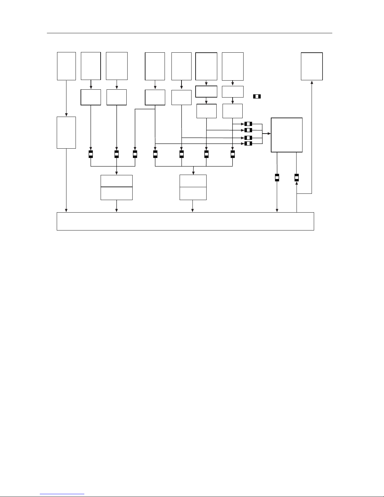
Figure 5. sbRIO-9687 Analog Input Subsystem
Over-Range
Comparators
DIO
Current-
Sensing
Resistor
DC Link Voltage
Phase Current
Differential
Amplifier
Bipolar to
Unipolar
CM
Filter
Simultaneous AI
Thermistor
Connector
Inverter
Connectors
Breakout
Connector
Scanned AI Scanned AI
Temp
Signals
External
Slow AI
UDC
Signals
I Phase
Signals
External
Fast AI
External
Fast AI
AO
Configurable Position
Low Pass
Filter
Gain
Stage
CurrentSensing
Resistor
CM
Filter
CM
Filter
CM
Filter
CM
Filter
CM
Filter
Inverter
Connectors
Inverter
Connectors
Breakout
Connector
Breakout
Connector
Breakout
Connector
Thermistor
Circuit
Temperature
Configuration
Resistors or Contacts
AO
GPIC
Simultaneous Sampled Analog Input
The General Purpose Inverter Controller (GPIC) has 16 simultaneous sampling analog inputs,
which acquire samples at a rate of 180 kS/s per channel. Phase difference between channels is
minimal due to the simultaneous sampling and high bandwidth of these signals. Each GPIC
input is differential with a software-range of ±10 V or ±5 V. These inputs should be used for
signals whose bandwidth and phase information is important for the control algorithm. Phase
current and DC link voltage from inverters can be connected to simultaneous sampled AI.
The sbRIO-9687 has 16 external analog inputs that can be connected to the GPIC
simultaneous sampling analog inputs. Other features of the analog input circuitry include:
• Pads for current-sensing resistor option on each input.
• Low pass filter and gain stage for each input.
• Eight configurable over-range comparators.
The following figure shows depicts a block diagram for simultaneous sampled analog input.
sbRIO-9687 User Manual | © National Instruments | 15
Page 16
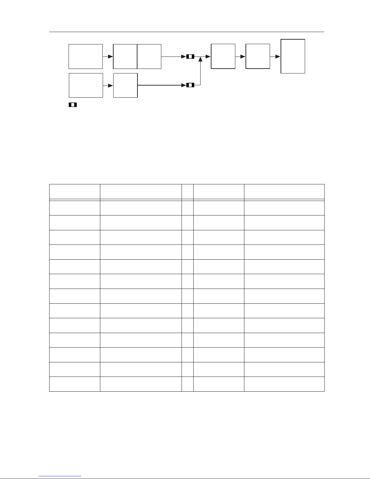
Figure 6. Simultaneous Sampled Analog Input
GPIC
Input
Connector
Inverter
Connectors
CurrentSensing
Resistor
Low
Pass
Filter
Gain
Stage
CM
Filter
ssAI
Phase Current
DC Link Voltage
CM
Filter
Configurable position
Simultaneous Analog Input Connectors
The sbRIO-9687 interface board includes 16 external simultaneous sampling analog inputs at
two connectors, J5 and J11. The following tables provide pin assignment information for the
J5 and J11 simultaneous AI breakout connectors.
Table 12. J5 Pin Assignments
Pin Signal Pin Signal
1 GND 14 GND
2 ssAI0+ 15 ssAI0–
3 ssAI1+ 16 ssAI1–
4 GND 17 GND
5 ssAI2+ 18 ssAI2–
6 ssAI3+ 19 ssAI3–
7 GND 20 GND
8 ssAI4+ 21 ssAI4–
9 ssAI5+ 22 ssAI5–
10 GND 23 GND
11 ssAI6+ 24 ssAI6–
12 ssAI7+ 25 ssAI7–
13 GND 26 GND
16 | ni.com | sbRIO-9687 User Manual
Page 17
Table 13. J11 Pin Assignments
Pin Signal Pin Signal
1 GND 14 GND
2 ssAI8+ 15 ssAI8–
3 ssAI9+ 16 ssAI9–
4 GND 17 GND
5 ssAI10+ 18 ssAI10–
6 ssAI11+ 19 ssAI11–
7 GND 20 GND
8 ssAI12+ 21 ssAI12–
9 ssAI13+ 22 ssAI13–
10 GND 23 GND
11 ssAI14+ 24 ssAI14–
12 ssAI15+ 25 ssAI15–
13 GND 26 GND
Connecting Voltage Sources to Simultaneous Analog Input
All sixteen inputs share a common ground that is the same as the digital and analog ground of
the GPIC. The differential input signal and absolute voltage of each input should be within the
input range of each channel. Refer to the sbRIO-9687 Specifications for details.
The simultaneous sampling analog inputs are differential, so the input measures the voltage
between the positive and negative terminals.
Figure 7. Connecting a Differential Voltage Signal to Simultaneous AI
+
–
+
–
Voltage
Source
Common
Mode
Voltage
Source
ssAI+
ssAI–
GND
ADC
sbRIO-9687
Gain
sbRIO-9683/9684
Termination
Resistor
Differential
Amplifier
Lowpass
Filter
AI+
AI–
sbRIO-9687 User Manual | © National Instruments | 17
Page 18

If single-ended signals are measured, one end of the signal source and one input terminal
should be connected to ground, as in the following diagram.
Figure 8. Connecting a Single-Ended Voltage Signal to Simultaneous AI
+
–
Voltage
Source
ssAI+
ssAI–
GND
ADC
sbRIO-9687
Gain
sbRIO-9683/9684
Differential
Amplifier
Lowpass
Filter
AI+
AI–
The gain stage of each input channel can be set as x1, x2, x3, or x4. See Gain Stage on page
22 for details.
Connecting Current Output Sensors to Simultaneous Analog
Input
A large selection of current output sensors can be connected to the sbRIO-9687. For current
measurements, a current-sensing resistor converts input current into voltage. The burden
voltage of the resistor follows the same signal path as the voltage inputs.
Figure 9. Connecting a Current Output Sensor to Simultaneous AI
ADC
sbRIO-9687
Gain
sbRIO-9683/9684
ssAI+
ssAI–
Current Output
Sensor
Power
Supply
PS+
PS–
Termination
Resistor
Differential
Amplifier
Lowpass
Filter
AI+
AI–
If the sensor is powered, the sensor power supply ground should be connected to the ground
pin on the simultaneous AI connector. The common mode and differential input signal on the
burden resistor should stay within the limits listed in the Simultaneous Sampled Analog Input
section of the sbRIO-9687 Specifications.
Current-Sensing Resistor
By default, the current-sensing resistor is not populated. The current-sensing resistor pads
accommodate a resistor footprint of 2512, with a maximum dissipated power of 1 W. For
lower power applications, the sbRIO-9687 includes a 1206 footprint (0.25 W) in parallel with
the current-sensing resistor.
18 | ni.com | sbRIO-9687 User Manual
Page 19

Select the current-sensing resistor value so that the power dissipation is minimized while as
much of the GPIC input range as possible is used. The current-sensing resistor value should be
less than or equal to the lesser of the values obtained from the following equations:
R
CSR_max
≤
P
CSR
I
in
_
rms
2
R
CSR
_
max
≤
GPIC
range
AI
gain
× I
in
_
max
where
P
CSR
= Current-sensing resistor power (1 W for 2512 footprint, 0.25 W for 1206
footprint).
R
CSR_max
= Maximum resistance of the current-sensing resistor (in Ohms).
I
in_rms
= RMS value of the input current (in Amps).
I
in_max
= Maximum input current (DC or
pk − pk
2
) (in Amps).
GPIC
range
= Input range set for the GPIC (10 V or 5 V).
AI
gain
= Gain of the interface board amplifier (x1, x2, x3, x4).
Note Use the maximum gain for simultaneous sampled analog input to get a lower
power dissipation from the current-sensing resistor.
Table 14. Simultaneous Sampled AI Current-Sensing Resistors
Simultaneous AI 2 W Current-Sensing Resistor 0.25 W Current-Sensing Resistor
ssAI0± R141 R140
ssAI1± R121 R120
ssAI2± R91 R90
ssAI3± R60 R59
ssAI4± R46 R45
ssAI5± R30 R29
ssAI6± R17 R16
ssAI7± R5 R4
ssAI8± R304 R303
ssAI9± R266 R265
sbRIO-9687 User Manual | © National Instruments | 19
Page 20

Table 14. Simultaneous Sampled AI Current-Sensing Resistors (Continued)
Simultaneous AI 2 W Current-Sensing Resistor 0.25 W Current-Sensing Resistor
ssAI10± R243 R242
ssAI11± R232 R231
ssAI12± R213 R212
ssAI13± R198 R197
ssAI14± R186 R185
ssAI15± R161 R160
Common Mode Filters
The sbRIO-9687 uses a high frequency common mode filter for each analog input from
external connectors and from Semikron modules. The common mode filter attenuates the
inverters' high frequency switching noise, which can interfere with the input signal.
Simultaneous Analog Input Configuration
The signal source for each GPIC simultaneous analog input is selected with a series of DIP
switches. Because all input signals are differential, a pair of contacts should be closed to select
one signal source. Refer to the following table for information about selecting simultaneous
sampled analog input signal source.
Table 15. Simultaneous Sampled Analog Input Signal Source Selection
Input 1 (Inverters) Input 2 (AI Connector)
GPIC Input Name Switch Contact Pair Name Switch Contact Pair
AI0± I Phase 0 SW42 3, 4 ssAI0± SW42 1, 2
AI1± I Phase 1 SW34 3, 4 ssAI1± SW34 1, 2
AI2± I Phase 2 SW36 3, 4 ssAI2± SW36 1, 2
AI3± I Phase 3 SW38 3, 4 ssAI3± SW38 1, 2
AI4± I Phase 4 SW44 3, 4 ssAI4± SW44 1, 2
AI5± I Phase 5 SW40 3, 4 ssAI5± SW40 1, 2
AI6± I Phase 6 SW25 3, 4 ssAI6± SW25 1, 2
AI7± U DC 0 SW41 3, 4 ssAI7± SW41 1, 2
AI8± U DC 1 SW33 3, 4 ssAI8± SW33 1, 2
20 | ni.com | sbRIO-9687 User Manual
Page 21

Table 15. Simultaneous Sampled Analog Input Signal Source Selection (Continued)
Input 1 (Inverters) Input 2 (AI Connector)
GPIC Input Name Switch Contact Pair Name Switch Contact Pair
AI9± U DC 2 SW35 3, 4 ssAI9± SW35 1, 2
AI10± U DC 3 SW37 3, 4 ssAI10± SW37 1, 2
AI11± U DC 4 SW43 3, 4 ssAI11± SW43 1, 2
AI12± U DC 5 SW39 3, 4 ssAI12± SW39 1, 2
AI13± U DC 6 SW24 3, 4 ssAI13± SW24 1, 2
AI14± — — — ssAI14± connected —
AI15± — — — ssAI15± connected —
Notice Only one signal source should be connected to each GPIC analog input at
one time. Connecting two signal sources in parallel can produce unexpected results.
Analog inputs from inverters are shared between the half-bridge modules and the full-bridge
modules. For proper operation, each analog line should be driven by only one inverter. Refer
to Inverter Signals on page 9 for more information.
Low Pass Filters
The sbRIO-9687 provides a low pass filter for each analog input. The filter has two stages that
are populated by default with 10 kΩ resistors and 3.3 nF capacitors. Refer to the sbRIO-9687
Specifications for details about the filter characteristics.
Figure 10. Simultaneous Sampled AI Input Low Pass Filter
From Input
Selection
To Gain
Stage
C1 C2
R1 R2
R1 R2
The first two filter resistors (R1) have a second functionality on the board and have a value of
10 kΩ. Other filter elements can be changed to set filter characteristics as required by the
application. The R2 has a default value of 10 kΩ (0603 footprint), and C1 and C2 have a
default value of 3.3 nF (0805 footprint).
sbRIO-9687 User Manual | © National Instruments | 21
Page 22

Table 16. Filter Component Reference Designators
GPIC Input R2 C1 C2
AI0± R195, R207 C122 C121
AI1± R219, R227 C142 C141
AI2± R219, R226 C140 C139
AI3± R194, R206 C120 C119
AI4± R183, R170 C105 C104
AI5± R138, R153 C88 C87
AI6± R169, R182 C103 C102
AI7± R137, R152 C86 C85
AI8± R68, R75 C47 C46
AI9± R107, R118 C70 C69
AI10± R99, R116 C66 C65
AI11± R80, R66 C50 C49
AI12± R38, R50 C31 C30
AI13± R12, R24 C14 C13
AI14± R49, R37 C29 C28
AI15± R23, R11 C12 C11
Note For a different cut-off frequency, change only the filter capacitors while
keeping C1 and C2 of equal value.
Gain Stage
Each analog input channel has a gain stage immediately after the low pass filter. Gain can be
set as x1, x2, x3, and x4. The output of the gain stage will work correctly only if the input
voltage at the simultaneous AI connector is within the common mode and differential range
listed in the sbRIO-9687 Specifications for each selected gain.
The gain should be set to use as much of the GPIC input range as possible. When current
signals are converted to voltage with onboard current-sensing resistors, it is preferable to set
the gain to the maximum value so that power dissipation from resistors is minimized.
Refer to the following tables for information regarding simultaneous sampled AI gain
configuration and related DIP switch reference designators and contact assignments.
22 | ni.com | sbRIO-9687 User Manual
Page 23

Table 17. Simultaneous Sampled AI Gain Configuration
Gain_A Contact Gain_B Contact Gain Input Range
open open x1 ±10 V
closed open x2 ±5 V
open closed x3 ±3.33 V
closed closed x4 ±2.5 V
Table 18. DIP Switch Reference Designators and Contact Assignments
GPIC Input Switch Reference Designator Gain_A Contact Gain_B Contact
AI0± SW9 3 4
AI1± SW9 1 2
AI2± SW8 3 4
AI3± SW8 1 2
AI4± SW6 3 4
AI5± SW6 1 2
AI6± SW5 3 4
AI7± SW5 1 2
AI8± SW4 3 4
AI9± SW4 1 2
AI10± SW3 3 4
AI11± SW3 1 2
AI12± SW2 3 4
AI13± SW2 1 2
AI14± SW1 3 4
AI15± SW1 1 2
Note For analog inputs that are connected to inverter current or voltage outputs,
the gain should be set to x1.
sbRIO-9687 User Manual | © National Instruments | 23
Page 24

Scanned Analog Input
The sbRIO-9683 or sbRIO-9684 GPIC controller has eight scanned analog inputs with an
input range of 0 V to 5 V. These inputs have limited bandwidth, and each input is read at a
slightly different time as it is scanned. These inputs should be used for slow analog signals as
temperature or DC voltages.
The sbRIO-9687 interface board connects slow analog inputs from inverter and breakout
connectors to the GPIC scanned AI. The signals are conditioned. The input range on the
sbRIO-9687 is 0 V to 10 V or -5 V to 5 V.
Figure 11. Scanned AI Block Diagram
Differential/
Single-Ended
Amplifier
Breakout
Connector
Temperature
External AI
UDC Input
scAI
GPIC
Configurable position
CM
Filter
CM
Filter
CM
Filter
Inverter
Connectors
Scanned Analog Input Connectors
The sbRIO-9687 interface board has seven external scanned analog inputs that are available at
breakout connector J14. The following table provides pinout information for the breakout
connector.
Table 19. J14 Pin Assignments
Pin Signal Pin Signal
1 GND 14 GND
2 AO0 15 AO1
3 AO2 16 AO3
4 GND 17 GND
5 AO4 18 AO5
6 AO6 19 AO7
7 scAI0 20 scAI0 GND
24 | ni.com | sbRIO-9687 User Manual
Page 25

Table 19. J14 Pin Assignments (Continued)
Pin Signal Pin Signal
8 scAI1 GND 21 scAI1
9 scAI2 22 scAI2 GND
10 scAI3 GND 23 scAI3
11 scAI4 24 scAI4 GND
12 scAI5 GND 25 scAI5
13 scAI6 26 scAI6 GND
The sbRIO-9687 uses scanned analog input 7 for thermistor measurement; it is not available
on the breakout connector.
Connecting Voltage Sources to Scanned Analog Input
The scanned analog inputs are single ended. One of the input pins is always ground. It is
recommended to connect the signal source to the ground pin assigned to each analog input.
Figure 12. Connecting a Voltage Signal to Scanned AI
+
–
Voltage
Source
ssAI
scAI_GND
ADC
sbRIO-9687 sbRIO-9683/9684
Single Ended/Bipolar
Scanned Analog Input Configuration
The input source for scanned analog inputs 0 to 6 is selected with the onboard DIP switches.
The signal source can be inverter temperature, inverter DC link voltage, or external voltage
from the input breakout connector. Refer to the following table for information about selecting
scanned analog input signal source.
sbRIO-9687 User Manual | © National Instruments | 25
Page 26
Table 20. Scanned Analog Input Signal Source Selection
Input 1 Input 2 Input 3
GPIC
Input
Name Switch Contact
Pair
Name Switch Contact
Pair
Name Switch Contact
Pair
AI_0 UDC 0 SW30 1, 2 Temp0 SW30 3, 4 scAI0 SW30 5, 6
AI_1 UDC 1 SW26 1, 2 Temp1 SW26 3, 4 scAI1 SW26 5, 6
AI_2 UDC 2 SW27 1, 2 Temp2 SW27 3, 4 scAI2 SW27 5, 6
AI_3 UDC 3 SW28 1, 2 Temp3 SW28 3, 4 scAI3 SW28 5, 6
AI_4 UDC 4 SW29 1, 2 Temp4 SW29 3, 4 scAI4 SW29 5, 6
AI_5 UDC 5 SW31 1, 2 Temp5 SW31 3, 4 scAI5 SW31 5, 6
AI_6 UDC 6 SW23 1, 2 Temp6 SW23 3, 4 scAI6 SW23 5, 6
Unipolar/Bipolar Mode Configuration
Each scanned analog input can be configured to accept unipolar or bipolar input voltages.
Refer to the sbRIO-9687 Specifications for details about the input range and accuracy for each
setting. Refer to the following table for information about configuring unipolar and bipolar
input voltages.
Table 21. Scanned Analog Input Unipolar/Bipolar Configuration
Unipolar Input (0 V to 10 V) Bipolar Input (-5 V to 5 V)
GPIC Input Switch Reference
Designator
Contact Switch Reference
Designator
Contact
AI0 SW12 1 SW12 2
AI1 SW12 3 SW12 4
AI2 SW11 1 SW11 2
AI3 SW11 3 SW11 4
AI4 SW13 1 SW13 2
AI5 SW13 3 SW13 4
AI6 SW14 1 SW14 2
Notice Only one configuration should be selected for each scanned analog input.
Selecting both unipolar/bipolar configuration at the same time will produce
unexpected results.
26 | ni.com | sbRIO-9687 User Manual
Page 27

Note Scanned analog inputs connected to inverters should be set to unipolar mode.
Analog Output
The analog outputs of the GPIC are connected directly to the breakout connector. See Scanned
Analog Input Connectors on page 24 for details. The following figure shows a block diagram
for analog output subsystem.
Figure 13. Analog Output Block Diagram
GPIC
AO
Breakout
Connector
Onboard
Functionality
Configurable position
Analog output can be used on the sbRIO-9687 to set over-range thresholds. See Over-Range
Comparators on page 28 for details about onboard functionality.
The analog output lines have the same specifications as the AO lines of the GPIC. For more
information, refer to NI 9683 User Manual and Specifications and NI 9684 User Manual and
Specifications.
Analog Output Configuration
Analog outputs can be disconnected from the onboard functionality by changing the
corresponding DIP switch to the OFF position. Refer to the following table for information
about analog output configuration.
Table 22. Analog Output Configuration
GPIC Analog Output SW21 Contact
AO0 1
AO1 2
AO2 3
AO3 4
AO4 5
AO5 6
sbRIO-9687 User Manual | © National Instruments | 27
Page 28

Table 22. Analog Output Configuration (Continued)
GPIC Analog Output SW21 Contact
AO6 7
AO7 8
Note Analog outputs that are used outside the sbRIO-9687 should be disconnected
from onboard functionality.
Over-Range Comparators
The sbRIO-9687 interface board has eight over-range comparators that can be connected to
analog input signals. The over-range comparators are triggered if the absolute value of the
input is over the set voltage. For example, if the threshold is set at 7 V, then the over range is
triggered if the input is over 7 V or under -7 V.
The following figure is a block diagram for the over-range circuits.
Figure 14. Over-Range Circuit Block Diagram
Input
Connectors
Inverter
Connectors
Phase Current
DC Link Voltage
Over Range
Set Point
AO
DIO
GPIC
Configurable position
Over-Range
Comparators
CM
Filter
CM
Filter
Current-
Sensing
Resistor
CM
Filter
The eight over-range comparators can be connected to inverter phase current, inverter DC link
voltage, or to one of the 16 simultaneous sampled analog inputs. The over-range threshold can
be set using one of the GPIC analog outputs or by populating a resistor divider on the board.
The over-range output is an active low digital signal connected to the GPIC low voltage TTL
inputs.
Note If any of the DIO lines (DIO0 to DIO7) are to be used for the extension
board, they should be disconnected from the onboard functionality by depopulating
the corresponding 0 Ω resistor. See LVTTL Lines on page 38 for details.
Over-Range Comparator Input Configuration
Over-range comparators are connected to the input source with a series of DIP switches.
Because all input signals are differential, a pair of contacts should be closed to select one
28 | ni.com | sbRIO-9687 User Manual
Page 29

signal source. Refer to the following tables for information about selecting over-range
comparator input signal source.
Table 23. Over-Range Comparator Input Selection, Inputs 1 and 2
Circuit Input 1 Switch Contacts Input 2 Switch Contacts
O-Ra 0 I Phase Inv. 0 SW47 5, 6 UDC Inv. 0 SW47 1, 2
O-Ra 1 I Phase Inv. 1 SW45 5, 6 UDC Inv. 1 SW45 1, 2
O-Ra 2 I Phase Inv. 2 SW48 5, 6 UDC Inv. 2 SW48 1, 2
O-Ra 3 I Phase Inv. 3 SW49 5, 6 UDC Inv. 3 SW49 1, 2
O-Ra 4 I Phase Inv. 4 SW50 5, 6 UDC Inv. 4 SW50 1, 2
O-Ra 5 I Phase Inv. 5 SW46 5, 6 UDC Inv. 5 SW46 1, 2
O-Ra 6 I Phase Inv. 6 SW32 5, 6 UDC Inv. 6 SW32 1, 2
O-Ra 7 — — — — — —
Table 24. Over-Range Comparator Input Selection, Inputs 3 and 4
Circuit Input 3 Switch Contacts Input 4 Switch Contacts
O-Ra 0 ssAI0± SW47 7, 8 ssAI7± SW47 3, 4
O-Ra 1 ssAI1± SW45 7, 8 ssAI8± SW45 3, 4
O-Ra 2 ssAI2± SW48 7, 8 ssAI9± SW48 3, 4
O-Ra 3 ssAI3± SW49 7, 8 ssAI10± SW49 3, 4
O-Ra 4 ssAI4± SW50 7, 8 ssAI11± SW50 3, 4
O-Ra 5 ssAI5± SW46 7, 8 ssAI12± SW46 3, 4
O-Ra 6 ssAI6± SW32 7, 8 ssAI13± SW32 3, 4
O-Ra 7 ssAI14± SW10 3, 4 ssAI15± SW10 1, 2
Setting the Over-Range Threshold
Analog input signals are connected to the over-range comparators before the gain stage, so the
threshold should be set in accordance with the signal level at the sbRIO-9687 input, which is
the breakout connector or inverter connector. The over-range circuit has a gain of 0.5 that
should be considered when setting the threshold.
The over-range threshold can be set by using the GPIC analog outputs or by populating an
onboard resistive divider.
To use the GPIC analog output for the set point, configure AO for onboard use; see Analog
Output Configuration on page 27 for details. For each over-range comparator, set the
sbRIO-9687 User Manual | © National Instruments | 29
Page 30

corresponding AO channel to the appropriate DC value. The comparator threshold is twice the
set AO voltage and acts for both positive and negative input voltages.
VAO=
V
tℎresℎold
2
Note If GPIC analog outputs are used for the over-range comparator set point, the
corresponding contact on switch SW21 should be turned ON.
If using the onboard resistors to set the over-range threshold, the analog outputs should be
disconnected from the onboard functionality. See Analog Output Configuration on page 27 for
configuration information. The set point is established by populating the corresponding
resistor for each channel. To calculate the resistor value, use the following formula:
R
tℎresℎold
=
V
tℎresℎold
10V − V
tℎresℎold
× 100kΩ
The following table provides threshold settings for the sbRIO-9687 over-range comparators.
Table 25. Over-Range Comparator Threshold Setting
Circuit Set Point 1 Set Point 2 Over-Range OUT
O-Ra 0 AO0 R381 DIO0
O-Ra 1 AO1 R383 DIO1
O-Ra 2 AO2 R373 DIO2
O-Ra 3 AO3 R386 DIO3
O-Ra 4 AO4 R394 DIO4
O-Ra 5 AO5 R396 DIO5
O-Ra 6 AO6 R403 DIO6
O-Ra 7 AO7 R244 DIO7
Note If any of the lines DIO0 to DIO7 are to be used for the extension board, they
should be disconnected from the onboard functionality by depopulating the
corresponding 0 Ω resistor. See LVTTL Lines on page 38 for details.
Sourcing Digital Input
The GPIC has 28 sourcing digital inputs grouped in two ports. Each of the sourcing digital
inputs is connected to a breakout connector on the sbRIO-9687 interface board. The DI lines
30 | ni.com | sbRIO-9687 User Manual
Page 31

used onboard can be disconnected from the sbRIO-9687 circuitry by depopulating the 0 Ω
resistors.
The following figure shows a block diagram for the sourcing digital input circuitry.
Figure 15. Sourcing Digital Input Block Diagram
Breakout
Connector
Onboard
Functionality
GPIC
Configurable position
DI Port 0
DI Port 1
The sourcing DI lines have the same specifications as the sourcing DI lines of the GPIC. Port 1
should be powered at the VI_P1 pin for proper operation. The digital input operates in the low
range or high range based on the VI_P1 voltage.
Note If no device is connected to the sourcing digital input, the channel registers as
OFF. If the input is connected to ground, the channel registers as ON.
Sourcing Digital Input Connector
Sourcing digital inputs are available at breakout connector J12. Refer to the following table for
pinout information.
Table 26. J12 Sourcing Digital Input Connector Pinout
Pin Signal Pin Signal
1 GND 19 GND
2 DI_P0.0 20 DI_P0.1
3 DI_P0.2 21 DI_P0.3
4 DI_P0.4 22 DI_P0.5
5 DI_P0.6 23 DI_P0.7
6 DI_P0.8 24 DI_P0.9
7 DI_P0.10 25 DI_P0.11
8 DI_P0.12 26 DI_P0.13
9 +24 V 27 +24 V
10 GND 28 GND
sbRIO-9687 User Manual | © National Instruments | 31
Page 32

Table 26. J12 Sourcing Digital Input Connector Pinout (Continued)
Pin Signal Pin Signal
11 DI_P1.2 29 DI_P1.3
12 DI_P1.4 30 DI_P1.5
13 DI_P1.6 31 DI_P1.7
14 DI_P1.8 32 DI_P1.9
15 DI_P1.10 33 DI_P1.11
16 DI_P1.12 34 DI_P1.13
17 GND 35 VI_P1
18 Not Connected 36 Not Connected
Sourcing Digital Input Configuration
Port 0 of the sourcing digital input is powered at +24 V through the sbRIO-9687 interface
board. This power is available at the DI connector on pins 9 and 27. The +24 V can be used to
power external circuits or port 1.
Port 1 is not powered from sbRIO-9687 interface board; it should be powered externally at a
voltage that matches the voltage levels of the application. Power for port 1 is connected at pins
18 and 36 of J12 connector.
Port 0 DI lines are used on the sbRIO-9687 interface board. For details, refer to Halt Signals
on page 36 and GPIO Signals on page 37. If Port 0 DI lines are not used for the application,
they can be disconnected from onboard functionality by depopulating the corresponding
resistor.
Note If port 0 sinking DI lines are used outside the sbRIO-9687, they should be
disconnected from onboard functionality.
The following table provides information about the onboard function and corresponding
resistor for sourcing DI signals.
Table 27. Sourcing Digital Input Signals
GPIC DI Signal Onboard Function Disconnecting Resistor
DI_P0.0 HALT0 R550
DI_P0.1 HALT1 R570
DI_P0.2 HALT2 R554
32 | ni.com | sbRIO-9687 User Manual
Page 33

Table 27. Sourcing Digital Input Signals (Continued)
GPIC DI Signal Onboard Function Disconnecting Resistor
DI_P0.3 HALT3 R535
DI_P0.4 HALT4 R516
DI_P0.5 HALT5 R633
DI_P0.6 HALT6 R566
DI_P0.7 GPIO0 R500
DI_P0.8 GPIO1 R501
DI_P0.9 GPIO2 R497
DI_P0.10 GPIO3 R498
DI_P0.11 GPIO4 R572
DI_P0.12 GPIO5 R499
DI_P0.13 GPIO6 R573
Sinking Digital Output
The GPIC has 24 sinking digital outputs. Each sinking DO is connected to the breakout
connector. The sbRIO-9687 interface board uses some of the DO lines, which can be
disconnected from sbRIO-9687 circuitry by depopulating 0 Ω resistors.
The sinking DO lines have the same electrical specifications as the DO lines of the GPIC. For
more information, refer to the NI 9683 User Manual and Specifications or the NI 9684 User
Manual and Specifications. The GPIC has current sinking digital outputs, which means that
the output pin is driven to ground (GND) when the channel is ON.
The following figure is a block diagram of the sinking digital output.
Figure 16. Sinking Digital Output Block Diagram
Breakout
Connector
Onboard
Functionality
GPIC
Configurable position
DO
sbRIO-9687 User Manual | © National Instruments | 33
Page 34

Sinking DO Connector
Sinking digital outputs are available at breakout connector J9. The following table contains
pinout information for the sinking DO connector.
Table 28. J9 Sinking Digital Output Pinout
Pin Signal Pin Signal
1 GND 19 GND
2 DO_0 20 DO_1
3 DO_2 21 DO_3
4 DO_4 22 DO_5
5 DO_6 23 DO_7
6 DO_8 24 DO_9
7 DO_10 25 DO_11
8 DO_12 26 DO_13
9 — 27 —
10 GND 28 GND
11 DO_14 29 DO_15
12 DO_16 30 DO_17
13 DO_18 31 DO_19
14 DO_20 32 DO_21
15 DO_22 33 DO_23
16 GND 34 GND
17 GND 35 GND
18 — 36 —
Sinking Digital Output Configuration
The first seven digital output lines are used on the sbRIO-9687 interface board for inverter
signals. See Inverter Digital Signals on page 35 for more details. If sinking digital outputs
need to be used externally, they can be disconnected from onboard functionality by
depopulating the corresponding resistors. The following table provides information about the
onboard function and corresponding resistor for sinking DO signals.
34 | ni.com | sbRIO-9687 User Manual
Page 35
Table 29. Sinking Digital Output Signals
GPIC DO Signal Onboard Function Resistor
DO_0 HALT0 R524
DO_1 HALT1 R552
DO_2 HALT2 R508
DO_3 HALT3 R534
DO_4 HALT4 R517
DO_5 HALT5 R632
DO_6 HALT6 R567
Inverter Digital Signals
Semikron inverters have several digital signals that can be read by and in some case written by
the GPIC. The functionality of the digital signals depends on the inverter type and is described
in Semikron documentation. The following tables provide information about the Semikron
inverter digital signal connections.
Table 30. Semikron Inverter Digital Signal Connections (Single-Phase Inverters)
Inverter
Connector
Signal
(Semikron)
R/W Inv. 0 Inv. 1 Inv. 2 Inv. 3 Inv. 4 Inv. 5 Inv. 6
SKiiP 4 CMM_HALT R/W HALT0 HALT1 HALT2 HALT3 HALT4 HALT5 HALT6
CMM_GPIO R GPIO0 GPIO1 GPIO2 GPIO3 GPIO4 GPIO5 GPIO6
CMM_GPIO2 R — — — — — — —
SKiiP 3
GB
ERROR out R HALT0 HALT1 HALT2 HALT3 HALT4 HALT5 HALT6
Overtemp out R GPIO0 GPIO1 GPIO2 GPIO3 GPIO4 GPIO5 GPIO6
SemikubeGBIF_CMN_nHALT R/W HALT0 HALT1 HALT2 HALT3 HALT4 HALT5 HALT6
IF_CMN_GPIO R/W GPIO0 GPIO1 GPIO2 GPIO3 GPIO4 GPIO5 GPIO6
sbRIO-9687 User Manual | © National Instruments | 35
Page 36

Table 31. Semikron Inverter Digital Signal Connections (Three-Phase Inverters)
Inverter Connector Signal (Semikron) Read/Write Inv. 0 Inv. 1
SKiiP 3 GD ERROR HB1 out R HALT0 HALT3
ERROR HB2 out R HALT1 HALT4
ERROR HB3 out R HALT2 HALT5
Overtemp out R GPIO0 GPIO5
Semikube SL GD IF_CMN_nHALT R/W HALT0 HALT5
IF_CMN_GPIO R GPIO0 GPIO5
Semikube GD IF_CMN_nHALT R/W HALT0 HALT5
Reserved R/W GPIO0 GPIO5
Halt Signals
The sbRIO-9687 HALT signals are bidirectional. Both ends of the signal line use a pull-up
resistor and a transistor for pull-down functionality. Both the controller and the inverter can set
or read the status of the signal line. The following diagram shows the HALT signal schematic.
Figure 17. HALT Signal Schematic
Vp
Write
Read
Inverter
sbRIO-9687
Vp
DI
DO
To read the line status, set the corresponding sinking digital output to high; the logic level will
be read on the corresponding sourcing digital input. To write to the line, set the sinking digital
output to low or high.
The following table shows the mapping between inverter HALT signals and GPIC sourcing
DO and sinking DI.
36 | ni.com | sbRIO-9687 User Manual
Page 37

Table 32. Mapping for HALT, Sourcing DO, and Sinking DI Signals
HALT Lines GPIC DI Line GPIC DO Line
HALT0 DI_P0.0 DO_0
HALT1 DI_P0.1 DO_1
HALT2 DI_P0.2 DO_2
HALT3 DI_P0.3 DO_3
HALT4 DI_P0.4 DO_4
HALT5 DI_P0.5 DO_5
HALT6 DI_P0.6 DO_6
GPIO Signals
The sbRIO-9687 GPIO signals are unidirectional. The signals can only be read by the GPIC.
On the inverter side, the signal has a pull-up to 24 V for SKiiP 4, Semikube GB, Semikube
GD, Semikube SL GD inverters, and it is open collector for SKiiP 3 GB and SKiiP 3 GD
inverters. The following figure is a schematic diagram of the GPIO signals.
Figure 18. GPIO Signal Schematic
+24 V
Write
+24 V
DI
Inverter
SKiiP 3
InvertersbRIO-9687 sbRIO-9687
+24 V
DI
Write
The GPIO signals can be read on one of the sourcing digital input lines. The following table
shows the mapping between inverter GPIO signals and GPIC sinking digital input.
Table 33. Mapping Between GPIO Signals and Sinking Digital Input
GPIO Line (Inverters) DI Line (GPIC)
GPIO0 DI_P0.7
GPIO1 DI_P0.8
GPIO2 DI_P0.9
GPIO3 DI_P0.10
sbRIO-9687 User Manual | © National Instruments | 37
Page 38

Table 33. Mapping Between GPIO Signals and Sinking Digital Input (Continued)
GPIO Line (Inverters) DI Line (GPIC)
GPIO4 DI_P0.11
GPIO5 DI_P0.12
GPIO6 DI_P0.13
LVTTL Lines
The sbRIO-9683 or sbRIO-9684 GPIC has 32 LVTTL digital signals. These signals are high
speed bidirectional lines with 3.3 V logical levels. All LVTTL lines are used for onboard
functions on the sbRIO-9687. All LVTTL signals are available at the two expansion board
connectors. The LVTTL signals are connected directly to the expansion board connectors and
have 0 Ω resistors to onboard functions.
The following figure shows a block diagram for the LVTTL lines.
Figure 19. LVTTL Lines Block Diagram
GPIC
LVTTL
Extension
Connector
Onboard
Functionality
Connector
Configurable position
The following table provides information about the onboard function and corresponding
resistor for the LVTTL lines.
Note It is highly recommended to disconnect the LVTTL signals from sbRIO-9687
functionality when they are being used with an expansion board.
Table 34. LVTTL Lines
GPIC Signal Onboard Function Direction (to
GPIC)
Active State Disconnecting
Resistor
DIO0 Over Range 0 Input Low R165
DIO1 Over Range 1 Input Low R156
DIO2 Over Range 2 Input Low R155
38 | ni.com | sbRIO-9687 User Manual
Page 39

Table 34. LVTTL Lines (Continued)
GPIC Signal Onboard Function Direction (to
GPIC)
Active State Disconnecting
Resistor
DIO3 Over Range 3 Input Low R150
DIO4 Over Range 4 Input Low R142
DIO5 Over Range 5 Input Low R134
DIO6 Over Range 6 Input Low R133
DIO7 Over Range 7 Input Low R129
DIO8 Feedback_0.0 Input Low/High R123
DIO9 Feedback_0.1 Input Low/High R114
DIO10 Feedback_0.2 Input Low/High R113
DIO11 Feedback_0.3 Input Low/High R104
DIO12 Feedback_0.4 Input Low/High R96
DIO13 Feedback_0.5 Input Low/High R95
DIO14 Hall_0.0 Input Low R86
DIO15 Hall_0.1 Input Low R78
DIO16 Hall_0.2 Input Low R65
DIO17 Feedback_1.0 Input Low/High R72
DIO18 Feedback_1.1 Input Low/High R73
DIO19 Feedback_1.2 Input Low/High R79
DIO20 Feedback_1.3 Input Low/High R87
DIO21 Feedback_1.4 Input Low/High R97
DIO22 Feedback_1.5 Input Low/High R98
DIO23 Hall_1.0 Input Low R105
DIO24 Hall_1.1 Input Low R115
DIO25 Hall_1.2 Input Low R124
DIO26 SCL (I2C RH sensor) Input/Output — R125
DIO27 SDA (I2C RH sensor) Input/Output — R130
sbRIO-9687 User Manual | © National Instruments | 39
Page 40

Table 34. LVTTL Lines (Continued)
GPIC Signal Onboard Function Direction (to
GPIC)
Active State Disconnecting
Resistor
DIO28 MUX A0 (TC Input) Output Low/High R135
DIO29 DS3 (Green LED) Output Low R136
DIO30 DS2 (Green LED) Output Low R143
DIO31 DS1 (Red LED) Output Low R151
The sbRIO-9683 LVTTL DIO lines connect directly to the FPGA DIO on the
sbRIO-9505/9506/9507 and are unbuffered and unprotected.
Caution Operating the LVTTL DIO outside the rated specifications may result in
permanent damage to the FPGA on the sbRIO-9605/9606/9607.
If overshoot, undershoot, and signal integrity are concerns for your application, use a single
load per line that does not exceed 25 pF.
The LVTTL DIO channels on the sbRIO-9687 are routed with a 50 Ω impedance trace. It is
recommended to route all external circuitry with a similar impedance to ensure the best signal
quality.
Expansion Board
LVTTL lines are available at two expansion connectors that allow a custom expansion board
to be placed on top of the sbRIO-9687 interface board.
Expansion Board Connectors
Each expansion board connector (J7 and J8) consists of a 26-pin header. For information about
mating connectors, refer to the Connectors on page 4 section. The following tables provide
pinout information for the expansion board connectors.
Table 35. LVTTL Expansion Connector Pinout (J7)
Pin Signal Pin Signal
1 DIO0 2 DIO1
3 DIO2 4 GND
5 DIO3 6 DIO4
7 GND 8 DIO5
40 | ni.com | sbRIO-9687 User Manual
Page 41

Table 35. LVTTL Expansion Connector Pinout (J7) (Continued)
Pin Signal Pin Signal
9 DIO6 10 DIO7
11 DIO8 12 GND
13 DIO9 14 DIO10
15 GND 16 DIO11
17 DIO12 18 DIO13
19 DIO14 20 GND
21 GND 22 DIO15
23 +3.3 V 24 +3.3 V
25 +5 V 26 +5 V
Table 36. LVTTL Expansion Connector Pinout (J8)
Pin Signal Pin Signal
1 DIO16 2 DIO17
3 DIO18 4 GND
5 DIO19 6 DIO20
7 GND 8 DIO21
9 DIO22 10 DIO23
11 DIO24 12 GND
13 DIO25 14 DIO26
15 GND 16 DIO27
17 DIO28 18 DIO29
19 DIO30 20 GND
21 GND 22 DIO31
23 +3.3 V 24 +3.3 V
25 +5 V 26 +5 V
sbRIO-9687 User Manual | © National Instruments | 41
Page 42

Expansion Board Power
The expansion board connectors have pins for +3.3 V and a +5 V power.
The +3.3 V is supplied directly by the GPIC, and the power is provided at the same time as the
sbRIO-9607 FPGA power. The current on the +3.3 V rail should not exceed 330 mA. For
details, refer to the NI sbRIO-9607 Specifications.
The +5 V pin is connected to the sbRIO-9687 internal rail and can supply up to 1 A for both
connectors.
Note A short circuit on the +5 V rail could shut down the sbRIO-9687 and may
require cycling the +24 V input.
Expansion Board Dimensions
An expansion board must have two mating connectors on the secondary side, each with pin 1
located as shown in the following figure.
Figure 20. Expansion Board Dimensions
4.5 in (114.3 mm)
2x 4.3 in (109.22 mm)
Pin 1 Location
26 POS 0.1” Pin Receptacles
Placed Bottom Side
1.55 in (39.37 mm)
2x .0 in (0 mm)
.2 in (5.08 mm)
.2 in (5.08 mm)
2x .0 in (0 mm)
2x 6.68 in (169.67 mm)
6.88 in (174.75 mm)
1.14 in (28.85 mm)
5.54 in (140.82 mm)
2.75 in (69.85 mm)
Top Side Shown
Feedback Input
The sbRIO-9687 interface board includes two connectors for feedback signals. Each connector
has six RS485 digital inputs for quadrature encoders, named Feedback_x.x_x, and three
inputs for open collector Hall sensors, named Hall_x.x.
Feedback Connectors
The following tables provide pinout information for the J6 and J10 feedback connectors.
42 | ni.com | sbRIO-9687 User Manual
Page 43

Table 37. J6 Feedback Connector Pinout
Pin Signal Pin Signal
1 GND 13 GND
2 Feedback_0.0_A 14 Feedback_0.0_B
3 Feedback_0.1_A 15 Feedback_0.1_B
4 Feedback_0.2_A 16 Feedback_0.2_B
5 GND 17 GND
6 Feedback_0.3_A 18 Feedback_0.3_B
7 Feedback_0.4_A 19 Feedback_0.4_B
8 Feedback_0.5_A 20 Feedback_0.5_B
9 GND 21 GND
10 Hall_0.0 22 Hall_0.1
11 Hall_0.2 23 GND
12 +5 V 24 +5 V
Table 38. J10 Feedback Connector Pinout
Pin Signal Pin Signal
1 GND 13 GND
2 Feedback_1.0_A 14 Feedback_1.0_B
3 Feedback_1.1_A 15 Feedback_1.1_B
4 Feedback_1.2_A 16 Feedback_1.2_B
5 GND 17 GND
6 Feedback_1.3_A 18 Feedback_1.3_B
7 Feedback_1.4_A 19 Feedback_1.4_B
8 Feedback_1.5_A 20 Feedback_1.5_B
9 GND 21 GND
10 Hall_1.0 22 Hall_1.1
sbRIO-9687 User Manual | © National Instruments | 43
Page 44

Table 38. J10 Feedback Connector Pinout (Continued)
Pin Signal Pin Signal
11 Hall_1.2 23 GND
12 +5 V 24 +5 V
See the LVTTL Lines on page 38 section for more information on how feedback signals are
connected to the GPIC digital lines.
RS485 Input Signals
RS485 input signals are used for interfacing with a large selection of encoders. Differential
RS485 signals are connected between the Feedback_x.x_A and Feedback_x.x_B lines. Each
input line can support up to ±25 V fault voltage. In normal operating mode, the input voltage
should be kept within the RS485 specifications.
The outputs of the RS485 receivers are directed to the LVTTL lines. The name of the
corresponding LVTTL signal is Feedback_x.x. For details, refer to LVTTL Lines on page
38.
Hall Sensor Input Signals
Each of the six Hall sensor inputs are designed for open collector driving outputs. Each input
has a 10 kΩ pull-up resistor connected to +5 V. The inputs have a Schmitt trigger input circuit
that reduces the false transitions for a noisy input signal. The output of the Schmitt trigger
circuit is connected to the LVTTL signals. For details, refer to LVTTL Lines on page 38.
+5 V Output
The feedback connectors have an +5 V output that can be used for powering encoders. The
+5 V output is connected to the sbRIO-9687 internal rail and can supply up to 0.5 A for each
connector.
Note A short circuit on the +5 V rail could shut down the sbRIO-9687 and may
require cycling the +24 V input.
Debug LEDs
The sbRIO-9687 interface board provides four LEDs for debugging purposes. One LED is
powered by the 5 V rails, and the others are driven by the LVTTL lines. The LED turns ON
when the corresponding LVTTL line is low. The following table provides information for each
LED, including reference indicator, color and LVTTL command line.
44 | ni.com | sbRIO-9687 User Manual
Page 45

Table 39. LED Command Lines
LED Reference Indicator LED Color LVTTL Command Line
DS1 RED DIO31
DS2 GREEN DIO30
DS3 GREEN DIO29
DS4 GREEN Always On
Thermistor
The sbRIO-9687 has support for two 10 kΩ thermistors for temperature measurement. The
sensors are connected to a 2.5 V reference through a 10 kΩ precision resistor. The thermistor
voltage is amplified by a factor of 2 on a gain stage, and then directed to the GPIC scanned
analog inputs.
Figure 21. Thermistor Measurement Circuit
ADCx2
sbRIO-9687 sbRIO-9683/9684
GAIN
Differential
Amplifier
scAI
GNDGND
Therm
Thermistor
10kΩ
2.5V
Reference
The thermistors should be connected between the two available terminals, Therm and
Therm_GND.
Caution Do not electrically connect the thermistor body to the chassis ground or to
high voltage lines in the cabinet. Such a connection could permanently damage the
sbRIO-9687.
Thermistor Connector
The following table provides pinout information for the thermistor connector. If a shielded
cable is used for the thermistor, connect the shield to the CHASSIS GND pins.
sbRIO-9687 User Manual | © National Instruments | 45
Page 46

Table 40. J28 Thermistor Input
Pin Signal Pin Signal
1 Therm1 4 Therm0
2 Therm1_GND 5 Therm0_GND
3 CHASSIS GND 6 CHASSIS GND
Thermistor Reading
The two thermistor outputs are multiplexed into the GPIC scanned AI_7 with the help of one
LVTTL line. When the LVTTL line is 0, the Therm0 signal is connected to AI_7. When the
LVTTL line is 1, the Therm1 signal is connected to AI_7.
DIO29 AI_7 Input
0 Thermocouple 0 input (Therm0)
1 Thermocouple 1 input (Therm1)
The following formula describes how the thermistor value can be obtained from the scanned
AI voltage:
R
Tℎermistor
=
V
AI_7
5V − V
AI_7
× 10 kΩ
where
R
Thermistor
= Thermistor resistance.
V
AI_7
= Voltage reading at the GPIC scanned AI_7.
To obtain the temperature, the thermistor value must be converted into temperature units based
on the typical thermistor characteristics obtained from thermistor manufacturer.
Relative Humidity Sensor
For safety, a high voltage system should not be operated when condensation conditions are
present. The sbRIO-9687 interface board has a built-in environmental sensor that measures
temperature and relative humidity (RH) on the board.
Use the following formula to determine the RH on a different point of the cabinet:
RH
cabinet
= RH
board
× e
17.502 × T
board
240.97 + T
board
−
17.502 × T
cabinet
240.97 + T
cabinet
46 | ni.com | sbRIO-9687 User Manual
Page 47
where
RH
cabinet
= RH value at a given point inside the cabinet (%).
T
cabinet
= Temperature at the point where we want to determine the RH (˚C).
RH
board
= RH value read from the onboard RH sensor (%).
T
board
= Temperature read from the onboard RH sensor (˚C).
The RH sensor type is HDC1080 (Texas Instruments). It communicates with the GPIC through
an I2C bus connected to the LVTTL lines. The following table shows the signal assignments
for the RH sensor. Consult the Texas Instruments Web site for a full description of the RH
sensor communication protocol.
Table 41. RH Sensor I2C Lines
I2C Signal LVTTL Line
SCL DIO26
SDA DIO27
Relay Connector
The sbRIO-9687 provides connections for four relay control outputs. Each output has a relay
control DO+ and a current return pin, relay control DO-. The sbRIO-9683 and sbRIO-9684
have current sinking outputs, which means that the relay control DO+ is driven to relay control
DO- when the channel is ON.
The following table provides pinout information for the relay connector.
Table 42. J4 Relay Connector Pinout
Pin Signal Pin Signal
1 +24 V 7 +24 V
2 DO0– 8 DO0+
3 DO1– 9 DO1+
4 DO2– 10 DO2+
5 DO3– 11 DO3+
6 GND 12 GND
The relay control lines are directly connected to the GPIC relay control connector. For further
details regarding best practices for relay connections, refer to the NI 9683 User Manual and
Specifications and the NI 9684 User Manual and Specifications.
sbRIO-9687 User Manual | © National Instruments | 47
Page 48

Display Connector
The sbRIO-9687 interface board includes support to drive an Amulet Technologies display
4
that connects to sbRIO using an RS232 interface. The sbRIO-9687 provides power for the
display on a separate connector.
The following tables provide pinout information for the RS232 and power connectors.
Table 43. J23 RS232 Serial Communication Connector
Connector Pin Signal Name
1 DCD
2 RXD
3 TXD
4 DTR
5 GND
6 DSR
7 RTS
8 CTS
9 RI
Table 44. J15 Display Power Connector
Connector Pin Signal Name
1 +5 V
2 GND
The maximum current available at the display power connector is 0.5 A.
Note The RS232 connector has a standard pinout and could be used for other needs
inside the system.
Inverter Connectors
The following tables provide pinout information for the inverter connectors.
4
NI part numbers 783304-01 (display), 783306-01 (power board), and 157570-01 (cable).
48 | ni.com | sbRIO-9687 User Manual
Page 49

Table 45. SKiiP 4 Connector (Dsub 25 Header)
Pin Signal Name Description
1 +24 V Power for inverter
2 +24 V Power for inverter
3 +24 V Power for inverter
4 CMN_rsvd Digital output signal from inverter (reserved)
5 HALT Halt signal
6 Temp Temperature (analog signal)
7 UDC DC link voltage (analog output)
8 HB_TOP Driving signal for high side IGBT
9 Rsvd Reserved
10 HB_I Phase current (analog output)
11 CAN_H CAN high
12 CAN_H CAN high
13 GND Ground
14 GND Ground
15 GND Ground
16 GND Ground
17 GND Ground
18 GPIOx General purpose digital output (open collector)
19 Temp_GND Return for temperature output
20 UDC_GND Return for DC link voltage
21 HB_BOT Driving signal for low side IGBT
22 GND Ground
23 HB_I_GND Return for Phase current output
24 CAN_L CAN low
sbRIO-9687 User Manual | © National Instruments | 49
Page 50

Table 45. SKiiP 4 Connector (Dsub 25 Header) (Continued)
Pin Signal Name Description
25 CAN_L CAN low
Shell Earth Earth ground
Table 46. Semikube GB Connector (20-pin DIN Header)
Pin Signal Name Description
1 +24 V Power for inverter
2 GND Ground
3 +24 V Power for inverter
4 GND Ground
5 +24 V Power for inverter
6 GND Ground
7 CMN_rsvd Digital output signal from inverter (reserved)
8 GND Ground
9 HALT Halt signal
10 GPIO General purpose digital output (open collector)
11 Temp Temperature (analog signal)
12 Temp_GND Return for temperature output
13 UDC DC link voltage (analog output)
14 UDC_GND Return for DC link voltage
15 HB_TOP Driving signal for high side IGBT
16 HB_BOT Driving signal for low side IGBT
17 Rsvd Reserved
18 GND Ground
19 HB_I Phase current (analog output)
20 HB_I_GND Return for phase current output
50 | ni.com | sbRIO-9687 User Manual
Page 51

Table 47. SKiiP 3 GB Connector (14-pin DIN Header)
Pin Signal Name Description
1 Earth Earth Ground
2 HB_BOT Driving signal for low side IGBT
3 HALT Halt signal
4 HB_TOP Driving signal for high side IGBT
5 GPIO General purpose digital output (open collector)
6 +24 V Power for inverter
7 +24 V Power for inverter
8 — Not connected
9 — Not connected
10 GND Ground
11 GND Ground
12 Temp/UDC Temperature or DC link voltage analog output (default to temperature)
13 AO_GND Return for phase current/temperature/DC link voltage output
14 HB_I Phase current (analog output)
Table 48. Semikube GD and Semikube SL GD Connector (34-pin DIN Header)
Pin Signal Name Description
1 +24 V Power for inverter
2 GND Ground
3 +24 V Power for inverter
4 GND Ground
5 +24 V Power for inverter
6 GND Ground
7 CMN_rsvd Digital output signal from inverter (reserved)
8 GND Ground
9 HALT Halt signal
sbRIO-9687 User Manual | © National Instruments | 51
Page 52

Table 48. Semikube GD and Semikube SL GD Connector (34-pin DIN
Header) (Continued)
Pin Signal Name Description
10 GPIO General purpose digital output (open collector)
11 Temp Temperature (analog signal)
12 Temp_GND Return for temperature output
13 UDC DC link voltage (analog output)
14 UDC_GND Return for DC link voltage
15 HB0_TOP Driving signal for high side IGBT (Half-Bridge 0)
16 HB0_BOT Driving signal for low side IGBT (Half-Bridge 0)
17 Rsvd Reserved
18 GND Ground
19 HB0_I Phase current output (Half-Bridge 0)
20 HB0_I_GND Return for phase current (Half-Bridge 0)
21 HB1_TOP Driving signal for high side IGBT (Half-Bridge 1)
22 HB1_BOT Driving signal for low side IGBT (Half-Bridge 1)
23 Rsvd Reserved
24 GND Ground
25 HB1_I Phase current output (Half-Bridge 1)
26 HB1_I_GND Return for phase current (Half-Bridge 1)
27 HB2_TOP Driving signal for high side IGBT (Half-Bridge 2)
28 HB2_BOT Driving signal for low side IGBT (Half-Bridge 2)
29 Rsvd Reserved
30 GND Ground
31 HB2_I Phase current output (Half-Bridge 2)
32 HB2_I_GND Return for phase current (Half-Bridge 2)
33 CAN_H CAN high
34 CAN_L CAN low
52 | ni.com | sbRIO-9687 User Manual
Page 53

Table 49. SKiiP 3 GD Connector (34-pin DIN Header)
Pin Signal Name Description
1 Earth Earth Ground
2 HB0_BOT Driving signal for low side IGBT (Half-Bridge 0)
3 HALT0 Halt signal (Half-Bridge 0)
4 HB0_TOP Driving signal for high side IGBT (Half-Bridge 0)
5 HB1_BOT Driving signal for low side IGBT (Half-Bridge 1)
6 HALT1 Halt signal (Half-Bridge 1)
7 HB1_TOP Driving signal for high side IGBT (Half-Bridge 1)
8 HB2_BOT Driving signal for low side IGBT (Half-Bridge 2)
9 HALT2 Halt signal (Half-Bridge 2)
10 HB2_TOP Driving signal for high side IGBT (Half-Bridge 2)
11 GPIO General purpose digital output (open collector)
12 — Not connected
13 UDC DC link voltage (analog output)
14 +24 V Power for inverter
15 +24 V Power for inverter
16 — Not connected
17 — Not connected
18 GND Ground
19 GND Ground
20 Temp Temperature (analog signal)
21 HB0_I_GND Return for phase current (Half-Bridge 0)
22 HB0_I Phase current output (Half-Bridge 0)
23 HB1_I_GND Return for phase current (Half-Bridge 1)
24 HB1_I Phase current output (Half-Bridge 1)
sbRIO-9687 User Manual | © National Instruments | 53
Page 54

Table 49. SKiiP 3 GD Connector (34-pin DIN Header) (Continued)
Pin Signal Name Description
25 HB2_I_GND Return for phase current (Half-Bridge 2)
26 HB2_I Phase current output (Half-Bridge 2)
Worldwide Support and Services
The NI website is your complete resource for technical support. At ni.com/support, you have
access to everything from troubleshooting and application development self-help resources to
email and phone assistance from NI Application Engineers.
Visit ni.com/services for information about the services NI offers.
Visit ni.com/register to register your NI product. Product registration facilitates technical
support and ensures that you receive important information updates from NI.
A Declaration of Conformity (DoC) is our claim of compliance with the Council of the
European Communities using the manufacturer’s declaration of conformity. This system
affords the user protection for electromagnetic compatibility (EMC) and product safety. You
can obtain the DoC for your product by visiting ni.com/certification. If your product supports
calibration, you can obtain the calibration certificate for your product at ni.com/calibration.
NI corporate headquarters is located at 11500 North Mopac Expressway, Austin, Texas,
78759-3504. NI also has offices located around the world. For support in the United States,
create your service request at ni.com/support or dial 1 866 ASK MYNI (275 6964). For
support outside the United States, visit the Worldwide Offices section of ni.com/niglobal to
access the branch office websites, which provide up-to-date contact information.
Information is subject to change without notice. Refer to the NI Trademarks and Logo Guidelines at ni.com/trademarks for
information on NI trademarks. Other product and company names mentioned herein are trademarks or trade names of their
respective companies. For patents covering NI products/technology, refer to the appropriate location: Help»Patents in your
software, the patents.txt file on your media, or the National Instruments Patent Notice at ni.com/patents. You can find
information about end-user license agreements (EULAs) and third-party legal notices in the readme file for your NI product. Refer
to the Export Compliance Information at ni.com/legal/export-compliance for the NI global trade compliance policy and how
to obtain relevant HTS codes, ECCNs, and other import/export data. NI MAKES NO EXPRESS OR IMPLIED WARRANTIES AS
TO THE ACCURACY OF THE INFORMATION CONTAINED HEREIN AND SHALL NOT BE LIABLE FOR ANY ERRORS. U.S.
Government Customers: The data contained in this manual was developed at private expense and is subject to the applicable
limited rights and restricted data rights as set forth in FAR 52.227-14, DFAR 252.227-7014, and DFAR 252.227-7015.
© 2018—2019 National Instruments. All rights reserved.
377239B-01 April 9, 2019
 Loading...