

Page 1
NI PXI/PCI-5114 Specifications
8-Bit 250 MS/s Digitizer
This document lists the specifications for the NI PXI/PCI-5114 (NI 5114)
high-speed digitizer. Unless otherwise noted, these specifications are valid
for the following conditions:
• All filter settings
• All impedance selections
• Sample clock set to 250 MS/s
Typical values are representative of an average unit operating at room
temperature. Specifications are subject to change without notice. For the
most recent NI 5114 specifications, visit
To access the NI 5114 documentation, including the NI High-Speed
Digitizers Getting Started Guide, which contains functional descriptions
of the NI 5114 signals, navigate to Start»All Programs»National
Instruments»NI-SCOPE»Documentation.
Hot Surface If the NI 5114 has been in use, it may exceed safe handling temperatures and
cause burns. Allow the NI 5114 to cool before removing it from the PXI chassis or PC.
Refer to the Environment section for operating temperatures of this device.
ni.com/manuals.
Contents
Vertical.................................................................................................... 2
Analog Input (Channel 0 and Channel 1) ........................................ 2
Horizontal................................................................................................ 6
Sample Clock...................................................................................6
Phase-Locked Loop (PLL) Reference Clock...................................7
CLK IN (Sample Clock and Reference Clock Input,
Front Panel Connector) ................................................................. 8
Trigger..................................................................................................... 8
Reference (Stop) Trigger ................................................................. 8
TRIG (External Trigger, Front Panel Connector)............................ 10
PFI 0 and PFI 1 (Programmable Function Interface,
AUX Front Panel Connectors) ............................................................. 11
TClk Specifications................................................................................. 12
Page 2

Waveform Specifications ........................................................................13
Calibration ...............................................................................................14
Power .......................................................................................................14
Software...................................................................................................15
Environment ............................................................................................16
NI PXI-5114 .....................................................................................16
NI PCI-5114 .....................................................................................17
Safety, Electromagnetic Compatibility, and CE Compliance .................18
Safety................................................................................................18
Electromagnetic Compatibility.........................................................18
CE Compliance.................................................................................18
Environmental Management ............................................................19
Physical....................................................................................................19
Front Panel Connectors ....................................................................19
Dimensions and Weight ...................................................................20
Where to Go for Support .........................................................................22
Vertical
Analog Input (Channel 0 and Channel 1)
Specification Val ue Comments
Number of
Channels
Connector BNC —
Impedance and Coupling
Input
Impedance
Input Coupling AC, DC, GND AC coupling
NI PXI/PCI-5114 Specifications 2 ni.com
Two (simultaneously sampled) —
50 Ω ±1.5%
1MΩ ±1% in parallel with a typical capacitance of 26 pF
Software
selectable
available on
1MΩ only
Page 3
Specification Val ue Comments
Voltage Levels
Full Scale (FS)
Input Range and
Programmable
Vertical Offset
Maximum Input
Overload
Accuracy
50 Ω 1MΩ —
Range
(V
pk-pk
Vertical Offset
Range (V)
)
Range
(V
pk-pk
Vertical Offset
)
Range (V)
0.04 ±0.8 0.04 ±0.8
0.1 ±0.8 0.1 ±0.8
0.2 ±0.8 0.2 ±0.8
0.4 ±0.8 0.4 ±0.8
1 ±6.5 1.0 ±8.0
2 ±6.0 2.0 ±8.0
4 ±5.0 4.0 ±8.0
10 ±30
10 ±2.0
20 ±25
40 ±15
50 Ω 1MΩ —
7V
with |Peaks| ≤10 V |Peaks| ≤35 V
rms
Resolution 8 bits —
DC Accuracy
(Programmable
Vertical
Offset = 0 V)
Programmable
Vertical Offset
Accuracy
NI PXI-5114:
±(1.5% of Input + 0.3% of FS + 200 μV)
NI PCI-5114:
Within ±5 °C of
self-calibration
temperature
±(1.5% of Input + 0.3% of FS + 280 μV)
± 2% of offset setting Within ±5 °C of
self-calibration
temperature
DC Drift ±(0.03% of Input + 0.06% of FS + 40 μV) per °C —
Crosstalk,
Typical
≤–60 dB at 10 MHz
≤–45 dB at 100 MHz
CH 0 to/from
CH 1, External
Trigger to CH 0
or CH 1
© National Instruments Corporation 3 NI PXI/PCI-5114 Specifications
Page 4
Specification Val ue Comments
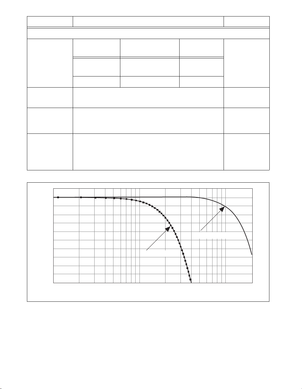
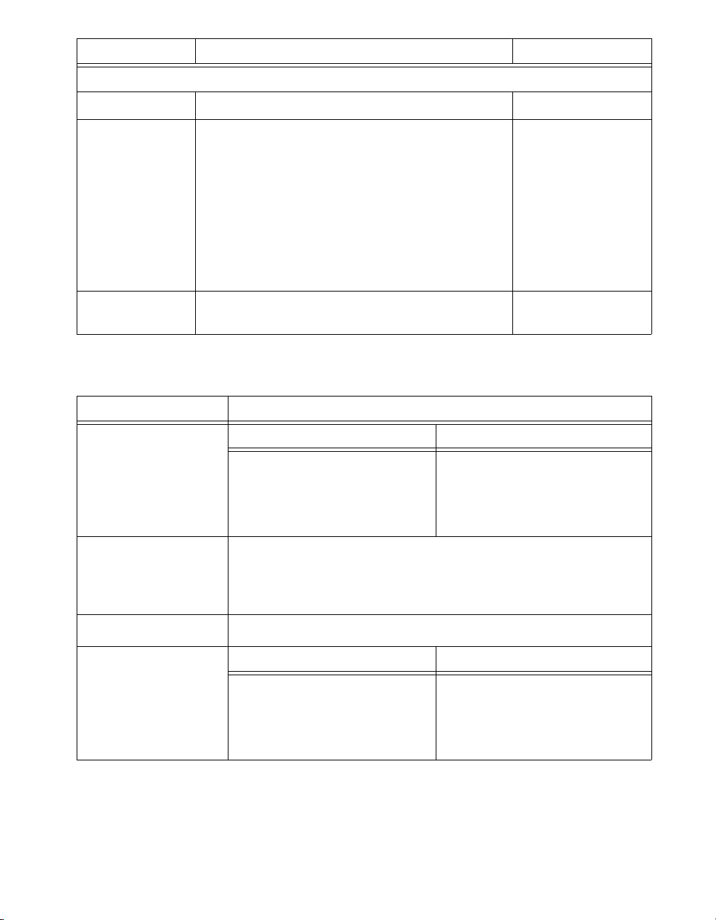
Bandwidth and Transient Response
Bandwidth
(–3 dB)
Bandwidth
Limit Filter
AC Coupling*
Cutoff (–3 dB),
Typical
Passband
Flatness
1
0
–1
–2
–3
–4
–5
–6
–7
–8
Amplitude (dB relative to 50 kHz)
–9
–10
1 M 100 M10 M 200 M
Range
(V
) Bandwidth
pk-pk
All ranges
125 MHz 2.8 ns
except 0.04
0.04 100 MHz 3.5 ns
20 MHz Noise Filter
12 Hz
±1 dB up to 50 MHz
Noise Filter
Frequency (Hz)
Rise/Fall Time,
Typical
Full Bandwidth
—
—
*AC coupling
available on
1MΩ only
Referenced to
50 kHz
Bandwidth
limit filter off
Figure 1. NI 5114 Frequency Response (Typical)
NI PXI/PCI-5114 Specifications 4 ni.com
Page 5

Specification Val ue Comments
Spectral Characteristics
Spurious-Free
Dynamic Range
with Harmonics
(SFDR), Typical
Total Harmonic
Distortion
(THD), Typical
Effective
Number of Bits
(ENOB),
Calculated*
Signal to Noise
and Distortion
(SINAD),
All ranges except 0.04 0.04
58 dBc 58 dBc
–58 dBc –58 dBc
7.2 6.2
44 dB 38 dB
Range (V
) 10 MHz,
pk-pk
–1 dBFS
input signal
Includes the
nd
2
the 5
harmonics
Measured
from DC to
125 MHz
20 MHz
bandwidth
limit filter off
Typical
RMS Noise Range
(V
pk-pk
All ranges
except 0.04
)
20 MHz
Filter On
20 MHz
Filter Off
0.28% FS 0.28% FS
50 Ω
terminator
connected
to input
0.04 0.28% FS 0.45% FS
*
ENOB = log2(sinad) – ½log2(1.5) – log2(A/V)
where
sinad = the linear representation of SINAD
A = amplitude of the supplied sine wave during the test
V = (peak) full-scale range of the waveform recorder input
Refer to 1057-1994 IEEE Standard for Digitizing Waveform Recorders for information on equation derivation.
through
th
© National Instruments Corporation 5 NI PXI/PCI-5114 Specifications
Page 6
Horizontal
Sample Clock
Specification Val ue Comments
Sources Internal, Onboard Clock (internal VCXO)*
External, CLK IN (front panel SMB connector)
Onboard Clock (Internal VCXO)
Sample Rate
Range
Timebase
Frequency
Timebase
Accuracy
Real-Time Sampling
(Single Shot)
3.815 kS/s to 250MS/s* 250 MS/s to 5 GS/s in
250 MHz When not using
Not Phase-Locked to
Reference Clock
±25 ppm Equal to the Reference
Random Interleaved
Sampling (RIS)
increments of 250 MS/s
Phase-Locked to
Reference Clock
Clock accuracy
* Internal Sample
Clock is locked to the
Reference Clock or
derived from the
onboard VCXO
* Divide by n
decimation used
for all rates less than
250 MS/s
For more information
about Sample Clock
and decimation, refer
to the NI High-Speed
Digitizers Help.
External Sample
Clock
—
Sample Clock
Delay Range
Sample Clock
Delay Resolution
NI PXI/PCI-5114 Specifications 6 ni.com
±1 Sample Clock period —
≤20 ps —
Page 7
Specification Val ue Comments
External Sample Clock
Sources CLK IN (front panel SMB connector) —
Frequency
Range
Duty Cycle
Tolerance
50 MHz to 250 MHz Divide by n
decimation
available where
1 ≤ n ≤ 65,535
For more information
about Sample Clock
and decimation, refer
to the NI High-Speed
Digitizers Help.
45% to 55% —
Phase-Locked Loop (PLL) Reference Clock
Specification Val ue
Sources NI PXI-5114 NI PCI-5114
PXI_CLK10
(backplane connector
CLK IN
(front panel SMB connector)
)
RTS I 7
CLK IN
(front panel SMB connector)
Frequency
Range
Duty Cycle Tolerance 45% to 55%
Exported Reference
Clock Destinations
© National Instruments Corporation 7 NI PXI/PCI-5114 Specifications
1 MHz to 20 MHz in 1 MHz increments
Default of 10 MHz
The PLL Reference Clock frequency must be accurate to ±50 ppm
NI PXI-5114 NI PCI-5114
PFI <0..1> (front panel 9-pin
mini-circular DIN connector)
PXI_Trig <0..7> (backplane
connector)
PFI <0..1> (front panel 9-pin
mini-circular DIN connector)
RTSI <0..7>
Page 8

CLK IN (Sample Clock and Reference Clock Input, Front Panel Connector)
Specification Val ue
Input Voltage Range Sine wave: 0.65 V
Square wave: 0.2 V
Maximum Input
Overload
Impedance 50 Ω
Coupling AC
7V
with |Peaks| ≤10 V
rms
pk-pk
pk-pk
to 2.8 V
to 2.8 V
(0 dBm to 13 dBm)
pk-pk
pk-pk
Trigger
Reference (Stop) Trigger
Specification Val ue Comments
Trigger Types
and Sources
Edge, Window, Hysteresis,
Video, Digital, Immediate,
and Software
Type s Sources Refer to the
CH 0, CH 1, TRIG,
PXI_Trig<0..6>, PFI <0..1>,
PXIStarTrigger,
RTSI<0..6>, and Software
following
sections and to
NI High-Speed
Digitizers Help
for more
information.
Time
Resolution
Rearm Time TDC Rearm Time Holdoff set to 0
Holdoff From Rearm Time up to [(235 – 1) × (Sample Clock Period)] —
Trigger Delay From 0 up to [(235 – 1) – posttrigger samples] ×
NI PXI/PCI-5114 Specifications 8 ni.com
TDC Onboard Clock External Clock TDC = Time to
On 40 ps N/A
Off 4ns External Clock Period
On 10 μs
Off 2 μs
(1/sample rate), in seconds
Digital
Conversion
Circuit
—
Page 9

Specification Val ue Comments
Analog Trigger (Edge, Window, and Hysteresis Trigger Types)
Sources CH 0 (front panel BNC connector)
—
CH 1 (front panel BNC connector)
TRIG (front panel BNC connector)
Trigger Level
8 bits (1 in 256)
Resolution
Trigger Level
Range
Edge Trigger
CH 0, CH 1 TRIG (External Trigger) —
100% FS ±5 V
5% FS up to 100 MHz 0.5 V
up to 100 MHz
pk-pk
Sensitivity
Level
±5% FS up to 10 MHz ±0.5 V up to 10 MHz
Accuracy,
Typical
Jitter ≤65 ps rms —
Trigger Filters Low Frequency (LF) Reject High Frequency (HF) Reject —
50 kHz 50 kHz
Digital Trigger (Digital Trigger Type)
Sources NI PXI-5114 NI PCI-5114 —
PXI_Trig <0..6> (backplane
connector)
PFI <0..1> (front panel
RTS I <0..6 >
PFI <0..1> (front panel
SMB connector)
SMB connector)
PXI Star Trigger (backplane
connector)
Video Trigger (Video Trigger Type)
Sources CH 0 (front panel BNC connector)
—
CH 1 (front panel BNC connector)
TRIG (front panel BNC connector)
© National Instruments Corporation 9 NI PXI/PCI-5114 Specifications
Page 10

Specification Val ue Comments
Types Specific Line
Any Line
Specific Field
Standards SDTV: M-NTSC, B/G-PAL, SECAM, M-PAL
EDTV: 480i/59.94 fps, 480i/60 fps, 480p/59.94 Fps,
480p/60 Fps, 576i/50 fps, 576p/50 Fps
HDTV: 720p/50 Fps, 720p/59.94 Fps, 720p/60 Fps,
1080i/50 fps, 1080i/59.94 fps, 1080i/60 fps, 1080p/24 Fps
TRIG (External Trigger, Front Panel Connector)
Specification Va lu e
Connector BNC
Impedance 1MΩ in parallel with 22 pF
Coupling AC, DC
AC-Coupling Cutoff (–3 dB) 12 Hz
Input Voltage Range ±5 V
—
fps = fields per
second
Fps = Frames
per second
Maximum Input Overload |Peaks| ≤42 V
NI PXI/PCI-5114 Specifications 10 ni.com
Page 11

PFI 0 and PFI 1 (Programmable Function Interface, AUX Front Panel Connectors)
Specification Valu e
Connector 9-pin mini-circular DIN
Direction Bi-directional
As an Input (Trigger)
Destinations Start Trigger (Acquisition Arm)
Reference (Stop) Trigger
Arm Reference Trigger
Advance Trigger
Input Impedance 150 kΩ
V
IH
V
IL
Maximum Input Overload –0.5 V, 5.5 V
Maximum Frequency 25 MHz
As an Output (Event)
Sources Start Trigger (Acquisition Arm)
Output Impedance 50 Ω
Logic Type 3.3 V CMOS
Maximum Drive Current ±24 mA
Maximum Frequency 25 MHz
2.0 V
0.8 V
Reference (Stop) Trigger
End of Record
Done (End of Acquisition)
Probe Compensation (1 kHz, 50% duty cycle square wave,
PFI 1 only)
© National Instruments Corporation 11 NI PXI/PCI-5114 Specifications
Page 12

TClk Specifications
National Instruments TClk synchronization method and the NI-TClk driver
are used to align the sample clocks on any number of SMC-based modules
in a chassis. For more information about TClk synchronization, refer to the
NI-TClk Synchronization Help, which is located within the NI High-Speed
Digitizers Help.
• Specifications are valid for any number of modules installed in one
NI PXI-1042 chassis.
• All parameters set to identical values for each SMC-based module.
• Sample Clock set to 250 MS/s and all filters are disabled.
• For other configurations, including multichassis systems, contact
NI Technical Support at
Note Although you can use NI-TClk to synchronize nonidentical modules, these
specifications apply only to synchronizing identical modules.
Specification Va lu e Comments
Intermodule SMC Synchronization Using NI-TClk for Identical Modules (Typical)
Skew 500 ps Caused by clock and analog
ni.com/support.
path delay differences
No manual adjustment
performed
Skew After Manual
Adjustment
Sample Clock
Adjustment
Resolution
NI PXI/PCI-5114 Specifications 12 ni.com
<20 ps For information about
manual adjustment, refer
to the Synchronization
Repeatability Optimization
topic in the NI-TClk
Synchronization Help.
For additional help with the
adjustment process, contact
NI Technical Support at
ni.com/support.
<20 ps —
Page 13

Waveform Specifications
Specification Val ue Comments
Onboard Memory
Size
Minimum Record
Length
Number of
Pretrigger Samples
Number of
Posttrigger Samples
Maximum Number
of Records in
Onboard Memory
8 MB per Channel
Standard
64 MB per Channel
Option
256 MB per Channel
Option
1 Sample —
Zero up to full Record Length Single-record
Zero up to full Record Length Single-record
8 MB/channel 32,768 * It is possible
64 MB/channel 100,000*
256 MB/channel 100,000*
8 megasamples
per channel
64 megasamples
per channel
256 megasamples
per channel
—
mode and
multiple-record
mode
mode and
multiple-record
mode
to exceed these
numbers if you
fetch records while
acquiring data. For
more information,
refer to the
NI High-Speed
Digitizers Help.
Allocated Onboard
Memory per Record
© National Instruments Corporation 13 NI PXI/PCI-5114 Specifications
(Record Length × 1 byte/S) + 240 bytes,
rounded up to next multiple of 128 bytes
or
256 bytes, whichever is greater
—
Page 14

Calibration
Specification Val ue
Self-Calibration Self-calibration is done on software command. The calibration
corrects for gain, offset, compensated 1 MΩ attenuator, triggering,
and timing adjustment errors for all input ranges.
External Calibration
(Factory Calibration)
Interval for External
Calibration
Warm-Up Time 15 minutes
The external calibration calibrates the VCXO, gain, and the voltage
reference. Appropriate constants are stored in nonvolatile memory.
2 years
Power
Specification Typical Value
NI PXI-5114 NI PCI-5114
+3.3 VDC
+5 VDC 1.1 A 1.7 A
+12 VDC 250 mA 45 mA
–12 VDC 170 mA —
Total Power 13.32 W 14.32 W
840 mA 1.6 A
NI PXI/PCI-5114 Specifications 14 ni.com
Page 15

Software
Specification Va lu e
Driver Software NI PXI-5114: NI-SCOPE 2.9 or later
NI PCI-5114: NI-SCOPE 3.1 or later
NI-SCOPE is an IVI-compliant driver that allows you to configure,
control, and calibrate the NI 5114. NI-SCOPE provides application
programming interfaces for many development environments.
Application Software NI-SCOPE provides programming interfaces, documentation, and
examples for the following application development environments:
•LabVIEW
™
•LabWindows
• Measurement Studio
• Microsoft Visual C/C++
• Microsoft Visual Basic
/CVI
™
Interactive Soft Front
Panel and
Configuration
The Scope Soft Front Panel 2.3 or later supports interactive control of the
NI 5114. The Scope Soft Front Panel is included on the NI-SCOPE CD.
National Instruments Measurement & Automation Explorer (MAX) also
provides interactive configuration and test tools for the NI 5114. MAX is
included on the NI-SCOPE CD.
© National Instruments Corporation 15 NI PXI/PCI-5114 Specifications
Page 16

Environment
NI PXI-5114
Note To ensure that the NI PXI-5114 cools effectively, follow the guidelines in
the Maintain Forced Air Cooling Note to Users included in the NI PXI-5114 kit.
The NI PXI-5114 is intended for indoor use only.
Specification Valu e
Operating Temperature 0 ºC to +55 ºC in all NI PXI chassis except the following:
0 ºC to +45 ºC when installed in an NI PXI-1000/B or PXI-101x chassis
Meets IEC-60068-2-1 and IEC-60068-2-2
Storage Temperature –40 ºC to +71 ºC
Meets IEC-60068-2-1 and IEC-60068-2-2
Operating Relative
Humidity
Storage Relative
Humidity
Operating Shock 30 g, half-sine, 11 ms pulse
Storage Shock 50 g, half-sine, 11 ms pulse
Operating Vibration 5 Hz to 500 Hz, 0.31 g
Storage Vibration 5 Hz to 500 Hz, 2.46 g
Altitude 2,000 m maximum (at 25 °C ambient temperature)
10% to 90%, noncondensing
Meets IEC-60068-2-56
5% to 95%, noncondensing
Meets IEC-60068-2-56
Meets IEC-60068-2-27
Test profile developed in accordance with MIL-PRF-28800F
Meets IEC-60068-2-27
Test profile developed in accordance with MIL-PRF-28800F
rms
Meets IEC-60068-2-64
rms
Meets IEC-60068-2-64
Test profile exceeds requirements of MIL-PRF-28800F, Class B
Pollution Degree 2
NI PXI/PCI-5114 Specifications 16 ni.com
Page 17

NI PCI-5114
Note To ensure that the NI PCI-5114 cools effectively, make sure that the chassis in which
it is used has active cooling that provides at least some airflow across the PCI card cage.
To maximize airflow and extend the life of the device, leave any adjacent PCI slots empty.
Refer to the Maintain Forced Air Cooling Note to Users included in the NI PCI-5114 kit
for important cooling information. The NI PCI-5114 is intended for indoor use only.
Specification Valu e
Operating Temperature 0 ºC to +45 ºC
Meets IEC-60068-2-1 and IEC-60068-2-2
Storage Temperature –40 ºC to +71 ºC
Meets IEC-60068-2-1 and IEC-60068-2-2
Operating Relative
Humidity
Storage Relative
Humidity
10% to 90%, noncondensing
Meets IEC-60068-2-56
5% to 95%, noncondensing
Meets IEC-60068-2-56
Storage Shock 50 g, half-sine, 11 ms pulse
Meets IEC-60068-2-27
Test profile developed in accordance with MIL-PRF-28800F
Storage Vibration 5 Hz to 500 Hz, 2.46 g
rms
Meets IEC-60068-2-64
Test profile exceeds requirements of MIL-PRF-28800F, Class B
Altitude 2,000 m maximum (at 25 °C ambient temperature)
Pollution Degree 2
© National Instruments Corporation 17 NI PXI/PCI-5114 Specifications
Page 18

Safety, Electromagnetic Compatibility, and CE Compliance
Safety
This product is designed to meet the requirements of the following
standards of safety for electrical equipment for measurement, control,
and laboratory use:
• IEC 61010-1, EN 61010-1
• UL 61010-1, CSA 61010-1
Note For UL and other safety certifications, refer to the product label or visit ni.com/
certification
in the Certification column.
Electromagnetic Compatibility
, search by model number or product line, and click the appropriate link
This product is designed to meet the requirements of the following
standards of EMC for electrical equipment for measurement, control, and
laboratory use:
• EN 61326 EMC requirements; Minimum Immunity
• EN 55011 Emissions; Group 1, Class A
• CE, C-Tick, ICES, and FCC Part 15 Emissions; Class A
Note For EMC compliance, operate this device with RG223/U or equivalent shielded
cable. Operate according to product documentation
CE Compliance
This product meets the essential requirements of applicable European
Directives, as amended for CE marking, as follows:
• 2006/95/EC; Low-Voltage Directive (safety)
• 2004/108/EC; Electromagnetic Compatibility Directive (EMC)
Note Refer to the Declaration of Conformity (DoC) for this product for any additional
regulatory compliance information. To obtain the DoC for this product, visit
certification
in the Certification column.
NI PXI/PCI-5114 Specifications 18 ni.com
, search by model number or product line, and click the appropriate link
ni.com/
Page 19
Environmental Management
⬉ᄤֵᙃѻક∵ᶧࠊㅵ⧚ࡲ⊩ ˄Ё
˅
Ёᅶ᠋
National Instruments is committed to designing and manufacturing
products in an environmentally responsible manner. NI recognizes that
eliminating certain hazardous substances from our products is beneficial
not only to the environment but also to NI customers.
For additional environmental information, refer to the NI and the
Environment Web page at
environmental regulations and directives with which NI complies, as well
as any other environmental information not included in this document.
Waste Electrical and Electronic Equipment (WEEE)
EU Customers At the end of their life cycle, all products must be sent to a WEEE recycling
center. For more information about WEEE recycling centers and National Instruments
WEEE initiatives, visit
National Instruments
݇Ѣ
National InstrumentsЁRoHS
(For information about China RoHS compliance, go to
ni.com/environment/weee.htm.
Physical
ni.com/environment. This page contains the
RoHS
ヺড়Ё⬉ᄤֵᙃѻકЁ䰤ࠊՓ⫼ᶤѯ᳝ᆇ⠽䋼ᣛҸ
ড়㾘ᗻֵᙃˈ䇋ⱏᔩ
ni.com/environment/rohs_china
ni.com/environment/rohs_china
(RoHS)
DŽ
DŽ
.)
Front Panel Connectors
Label Function Connector Type Comments
CH 0 Analog Input BNC female —
CH 1 Analog Input BNC female
TRIG External Trigger BNC female
CLK IN Sample Clock Input and
Reference Clock Input
AUX I/O PFI 0, PFI 1 9-pin mini-circular DIN
© National Instruments Corporation 19 NI PXI/PCI-5114 Specifications
SMB jack
Page 20

NI PXI-5114 Front Panel Indicators
Label Function For more
ACCESS The ACCESS LED indicates the status of the PCI bus and
the interface from the NI PXI-5114 to the controller.
ACTIVE The ACTIVE LED indicates the status of the onboard
acquisition hardware of the NI PXI-5114.
Dimensions and Weight
NI PXI-5114
Dimensions 3U, One slot, PXI/cPCI Module
21.6 × 2.0 × 13.0 cm
(8.5 × 0.8 × 5.1 in.)
2.0 cm
(0.8 in.)
information,
refer to the
NI High-Speed
Digitizers Help.
13.0 cm
(5.1 in.)
21.6 cm
(8.5 in.)
Weight 455g (16oz)
NI PXI/PCI-5114 Specifications 20 ni.com
Page 21

NI PCI-5114
Dimensions 35.5 × 2.0 × 11.3 cm
(14.0 × 0.8 × 4.4 in.)
2.0 cm
(0.8 in.)
11.3 cm
(4.4 in.)
Weight 421 g (14.8 oz)
35.5 cm
(14.0 in.)
© National Instruments Corporation 21 NI PXI/PCI-5114 Specifications
Page 22

Where to Go for Support
The National Instruments Web site is your complete resource for technical
support. At
troubleshooting and application development self-help resources to email
and phone assistance from NI Application Engineers.
A Declaration of Conformity (DoC) is our claim of compliance with the
Council of the European Communities using the manufacturer’s
declaration of conformity. This system affords the user protection for
electronic compatibility (EMC) and product safety. You can obtain the DoC
for your product by visiting
supports calibration, you can obtain the calibration certificate for your
product at
National Instruments corporate headquarters is located at
11500 North Mopac Expressway, Austin, Texas, 78759-3504.
National Instruments also has offices located around the world to help
address your support needs. For telephone support in the United States,
create your service request at
instructions or dial 512 795 8248. For telephone support outside the United
States, contact your local branch office:
Australia 1800 300 800, Austria 43 662 457990-0,
Belgium 32 (0) 2 757 0020, Brazil 55 11 3262 3599,
Canada 800 433 3488, China 86 21 5050 9800,
Czech Republic 420 224 235 774, Denmark 45 45 76 26 00,
Finland 358 (0) 9 725 72511, France 01 57 66 24 24,
Germany 49 89 7413130, India 91 80 41190000, Israel 972 3 6393737,
Italy 39 02 413091, Japan 81 3 5472 2970, Korea 82 02 3451 3400,
Lebanon 961 (0) 1 33 28 28, Malaysia 1800 887710,
Mexico 01 800 010 0793, Netherlands 31 (0) 348 433 466,
New Zealand 0800 553 322, Norway 47 (0) 66 90 76 60,
Poland 48 22 3390150, Portugal 351 210 311 210, Russia 7 495 783 6851,
Singapore 1800 226 5886, Slovenia 386 3 425 42 00,
South Africa 27 0 11 805 8197, Spain 34 91 640 0085,
Sweden 46 (0) 8 587 895 00, Switzerland 41 56 2005151,
Taiwan 886 02 2377 2222, Thailand 662 278 6777,
Turkey 90 212 279 3031, United Kingdom 44 (0) 1635 523545
ni.com/support you have access to everything from
ni.com/calibration.
ni.com/certification. If your product
ni.com/support and follow the calling
NI PXI/PCI-5114 Specifications 22 ni.com
Page 23

National Instruments, NI, ni.com, and LabVIEW are trademarks of National Instruments Corporation.
Refer to the Terms of Use section on ni.com/legal for more information about National
Instruments trademarks. Other product and company names mentioned herein are trademarks or trad e
names of their respective companies. For patents covering National Instruments products, refer to the
appropriate location: Help»Patents in your software, the patents.txt file on your CD, or
ni.com/patents.
© 2005–2007 National Instruments Corporation. All rights reserved.
374179C-01 Aug07
 Loading...