

Page 1

Computer-Based
Instruments
NI 5401 User Manual
™
PXI /PCI Arbitrary Function Generator
NI 5401 User Manual
March 1999 Edition
Part Number 322419A-01
Page 2

Worldwide Technical Support and Product Information
www.natinst.com
National Instruments Corporate Headquarters
11500 North Mopac Expressway Austin, Texas 78759-3504 USA Tel: 512 794 0100
Worldwide Offices
Australia 03 9879 5166, Austria 0662 45 79 90 0, Belgium 02 757 00 20, Brazil 011 284 5011,
Canada (Ontario) 905 785 0085, Canada (Québec) 514 694 8521, China 0755 3904939, Denmark 45 76 26 00,
Finland 09 725 725 11, France 01 48 14 24 24, Germany 089 741 31 30, Hong Kong 2645 3186,
India 91805275406, Israel 03 6120092, Italy 02 413091, Japan 03 5472 2970, Korea 02 596 7456,
Mexico (D.F.) 5 280 7625, Mexico (Monterrey) 8 357 7695, Netherlands 0348 433466, Norway 32 27 73 00,
Singapore 2265886, Spain (Madrid) 91 640 0085, Spain (Barcelona) 93 582 0251, Sweden 08 587 895 00,
Switzerland 056 200 51 51, Taiwan 02 2377 1200, United Kingdom 01635 523545
For further support information, see the Technical Support Resources appendix. To comment on the
documentation, send e-mail to techpubs@natinst.com.
© Copyright 1999 National Instruments Corporation. All rights reserved.
Page 3

Important Information
Warranty
The NI 5401 is warranted against defects in materials and workmanship for a period of one year from the date of shipment,
as evidenced by receipts or other documentation. National Instruments will, at its opt ion, repair or replace equipment that
proves to be defective during the warranty period . T his w arran ty i ncludes part s and l abo r.
The media on which you receive National Instruments software are warranted not to fail to execute programming
instructions, due to defects in materials and work man ship, for a peri od of 90 d ays from da te o f sh ipm ent, as evi denced
by receipts or other documentation. National Instruments will, at its option, repair or replace software media that do not
execute programming instructions if National Instruments receives noti ce of su ch defect s d uring th e warranty perio d.
National Instruments does not warrant that the op eration of t he soft ware shall b e uni nterrup ted or erro r free.
A Return Material Authorization (RMA) number must b e ob tain ed fro m th e facto ry an d clearl y mark ed on t he outsi de
of the package before any equipment wil l be accepted for warranty work. National Instruments will pay the shippi ng costs
of returning to the owner parts which are covered by warran ty.
National Instruments believes that the information in this document is accurate. The document has been carefully
reviewed for technical accuracy. In the event that technical or typographical errors exist, National Instruments reserves
the right to make changes to subsequent editions of this document without prior notice to holders of this edition. The
reader should consult National Instruments if errors are suspected. In no event shall National Instruments be liable for
any damages arising out of or related to th is d ocum ent o r th e in form ation con tained in i t.
XCEPT AS SPECIFIED HEREIN
E
ANY WARRANTY OF MERCHANTABILITY OR FITNESS FOR A PARTICULAR PURPOSE
BY FAULT OR NEGLIGENCE ON THE PART OF NATIONAL INSTRUMENTS SHALL BE LIMITED TO THE AMOUNT THERETOFORE PAID BY THE
CUSTOMER
OR INCIDENTAL OR CONSEQUENTIAL DAMAGES, EVEN IF ADVISED OF THE POSSIBILITY THEREOF
National Instruments will apply regardless of the form of action, wh ether in con tract or tort , incl udin g n egli gen ce.
Any action against National Instruments must be brought within one year after the cause of action accrues. National
Instruments shall not be liable for any delay in performance due to causes beyond its reasonable control. The warranty
provided herein does not cover damages, defects, malfuncti ons, or s ervice failur es caused by own er’s fai lure to fol low
the National Instruments installation, operation, or maintenance instructions; owner’s modification of the product;
owner’s abuse, misuse, or negligent acts; and power failure or surges, fire, flood, accident, actions of third parties,
or other events outside reasonable control.
ATIONAL INSTRUMENTS WILL NOT BE LIABLE FOR DAMAGES RESULTING FROM LOSS OF DATA, PROFITS, USE OF PRODUCTS
. N
ATIONAL INSTRUMENTS MAKES NO WARRANTIES, EXPRESS OR IMPLIED, AND SPECIFICALLY DISCLAIMS
, N
Copyright
Under the copyright laws, this publication may not be reproduced or transmitted in any form, electronic or mechanical,
including photocopying, recording, storing in an information retrieval system, or translating, in whole or in part, without
the prior written consent of National Instruments Corporation.
USTOMER’S RIGHT TO RECOVER DAMAGES CAUSED
. C
. This limitation of the liability of
,
Trademarks
ComponentWorks™, CVI™, LabVIEW™, natinst.com™, PXI™, RTSI™, and VirtualBench™ are trademarks of
National Instruments Corporation.
Product and company names mentioned herein are trademarks or trade names of their respective companies.
WARNING REGARDING MEDICAL AND CLINICAL USE OF NATIONAL INSTRUMENTS PRODUCTS
National Instruments products are not designed with com ponent s and tes ting for a level o f reli ability suit abl e for use in
or in connection with surgical implants o r as cri tical co m ponent s i n any li fe su pp ort sy stem s wh ose fail ure t o pe rform
can reasonably be expected to cause s ignifi cant in ju ry to a hu m an. A ppli cations of Nation al In st rument s prod ucts
involving medical or clinical treatment can create a pot enti al for d eath or bod ily i njury caused b y p rodu ct fail ure, o r by
errors on the part of the user or application designer. Because each end-user system is customized and differs from
National Instruments testing platforms and because a user or application designer may use National Instruments products
in combination with other products in a m ann er no t ev alu ated or co ntem p lated b y N ati onal Ins trum ents , the user or
application designer is ultimately responsible for verifying and validating the suitability of National Instruments products
whenever National Instruments products are incorporated in a system or application, including, without limitation,
the appropriate design , pr ocess and safet y level of such syst em or ap plicat io n.
Page 4
Conventions
The following conventions are used in this manual:
» The » symbol leads you through nested menu items and dialog box options
to a final action. The sequence File»Page Setup»Options directs you to
pull down the File menu, select the Page Setup item, and select Options
from the last dialog box.
♦ The ♦ symbol indicates that the following text applies only to a specific
product, a specific operating system, or a specific software version.
This icon denotes a note, which alerts you to important information.
This icon denotes a caution, which advises you of precautions to take to
avoid injury, data loss, or a system crash.
This icon denotes a warning, which advises you of precautions to take to
avoid being electrically shocked.
bold Bold text denotes items that you must select or click on in the software,
such as menu items and dialog box options. Bold text also denotes
parameter names.
italic Italic text denotes variables, emphasis, a cross reference, or an introduction
to a key concept.
monospace Text in this font denotes text or characters that you should enter from the
keyboard. This font is also used for the proper names of functions,
variables, and filenames and extensions.
monospace italic
Italic text in this font denotes text that is a placeholder for a word or value
that you must supply.
Page 5

Contents
Chapter 1
Generating Functions
with the NI 5401
About Your NI 5401......................................................................................................1-1
Connecting Signals ........................................................................................................1-2
ARB Connector...............................................................................................1-3
SYNC Connector.............................................................................................1-3
PLL Ref Connector..........................................................................................1-4
Pattern Out Connector (PCI Only)..................................................................1-5
Connector Pin Assignments....................................................... .......1-5
Signal Descriptions...........................................................................1-6
SHC50-68 50-Pin Cable Connector ................................................................1-6
Software Options for Your NI 5401 ..............................................................................1-8
Software Included with Your NI 5401 ............................................................1-8
VirtualBench.....................................................................................1-8
NI-FGEN Instrument Driver.............................................................1-9
Additional National Instruments Development Tools.....................................1-9
LabVIEW..........................................................................................1-9
LabWindows/CVI.............................................................................1-10
ComponentWorks .............................................................................1-10
Using the Soft Front Panels to Generate Waveforms....................................................1-11
Generating Standard Functions .......................................................................1-11
Generating Multiple Frequencies in a Sequence.............................................1-13
Waveform Editor.............................................................................................1-15
Power-Up and Reset Conditions....................................................................................1-16
Chapter 2
Function Generator Operation
Generating Waveforms..................................................................................................2-2
Direct Digital Synthesis (DDS) .....................................................................................2-3
Frequency Hopping and Sweeping..................................................................2-4
Triggering ......................................................................................................................2-4
Trigger Sources ...............................................................................................2-4
Modes of Operation.........................................................................................2-5
Single Trigger Mode.........................................................................2-5
Continuous Trigger Mode.................................................................2-6
Stepped Trigger Mode ........................................ ..............................2-7
Analog Output................................................................................................................2-7
©
National Instruments Corporation v NI 5401 User Manual
Page 6

Contents
SYNC Output and Duty Cycle........................................................................2-9
Output Attenuation.................................................. ........................................2-9
Output Impedance.............................................................. .............................2-10
Output Enable ..................................... .............................................. ..............2-10
Pre-Attenuation Offset.................................................................................... 2-11
Phase-Locked Loops and Board Synchronization.........................................................2-11
Analog Filter Correction................................................................................................2-13
RTSI/PXI Trigger Lines................................................................................................2-14
Calibration.....................................................................................................................2-15
Appendix A
Specifications
Appendix B
Optional Accessories
Appendix C
Frequency Resolution and Lookup Memory
Appendix D
Technical Support Resources
Glossary
Index
Figures
Figure 1-1. NI 5401 I/O Connectors........................................................................ 1-2
Figure 1-2. Output Levels and Load Termination Using a
50 Ω Output Impedance........................................................................1-3
Figure 1-3. SYNC Output and Duty Cycle..............................................................1-4
Figure 1-4. NI 5401 50-Pin Digital Connector Pin Assignments............................ 1-5
Figure 1-5. SHC50-68 68-Pin Connector Pin Assignments....................................1-7
Figure 1-6. VirtualBench-FG Soft Front Panel for Function Generation................ 1-11
Figure 1-7. VirtualBench-FG General Settings Dialog Box for the NI 5401.......... 1-12
Figure 1-8. VirtualBench-FG Signals Settings Dialog Box for the NI 5401........... 1-12
Figure 1-9. VirtualBench-FG Load Waveform Dialog Box....................................1-13
Figure 1-10. VirtualBench-FG Frequency List Editor Dialog Box...........................1-14
Figure 1-11. Waveform Editor Soft Front Panel .......................................................1-15
NI 5401 User Manual vi www.natinst.com
Page 7

Table
Contents
Figure 2-1. NI 5401 Block Diagram ........................................................................2-1
Figure 2-2. Waveform Data Path Block Diagram....................................................2-2
Figure 2-3. DDS Building Blocks............................................................................2-3
Figure 2-4. Waveform Generation Trigger Sources ................................................2-5
Figure 2-5. Single Trigger Mode .............................................................................2-6
Figure 2-6. Continuous Trigger Mode.....................................................................2-6
Figure 2-7. Stepped Trigger Mode............................... ... .........................................2-7
Figure 2-8. Analog Output and SYNC Out Block Diagram....................................2-8
Figure 2-9. Waveform and Trigger Timings............................................................2-8
Figure 2-10. Output Attenuation Chain .....................................................................2-9
Figure 2-11. PLL Architecture for the NI 5401 for PCI ............................................2-12
Figure 2-12. PLL Architecture for the NI 5401 for PXI............................................2-12
Figure 2-13. Analog Filter Correction .......................................................................2-13
Figure 2-14. RTSI Trigger Lines and Routing for the NI 5401 for PCI....................2-14
Figure 2-15. PXI Trigger Lines, 10 MHz Backplane Oscillator, and
Routing for the NI 5401 for PXI ...........................................................2-14
Table 1-1. Digital Connector Signal Descriptions..................................................1-6
©
National Instruments Corporation vii NI 5401 User Manual
Page 8

Generating Functions
with the NI 5401
The NI 5401 User Manual describes the features, functions, and operation
of the NI 5401 arbitrary function generator. This device performs
comparably to standalone instruments while providing the flexibility of
computer-based operation.
About Your NI 5401
Thank you for buying a National Instruments NI 5401 arbitrary function
generator. The NI 5401 family consists of two different devices:
• NI 5401 for PCI
• NI 5401 for PXI
Your NI 5401 device has the following features:
• One 12-bit resolution output channel
• Up to 16 MHz sine and transistor-transistor logic (TTL) waveform
output
• Software-selectable output impedances of 50 Ω and 75 Ω
• Output attenuation levels from 0 to 73 dB
• Phase-locked loop (PLL) synchronization to external clocks
• Sampling rate of 40 MS/s
• Digital and analog filter
• 32-bit direct digital synthesis (DDS) for standard function generation
• External trigger input
• Real-Time System Integration (RTSI) and PXI triggers
1
All NI 5401 devices follow industry-standard Plug and Play specifications
on both buses and offer seamless integration with compliant systems.
Detailed specifications for the NI 5401 are in Appendix A, Specifications.
©
National Instruments Corporation 1-1 NI 5401 User Manual
Page 9
Chapter 1 Generating Functions with the NI 5401
Connecting Signals
Figure 1-1 shows the front panels for the NI 5401 for the PXI and PCI
buses. The front panel contains three types of connectors: BNC, SMB, and
50-pin very high-density SCSI (VHDSCSI). The main waveform is
generated through the connector labeled ARB.
LOCK
ACCESS
ARB OUT
SYNC OUT
EXT TRIG
PLL REF
ARB
SYNC
PLL IN
PXI PCI
PATTERN OUT
Figure 1-1.
NI 5401 I/O Connectors
NI 5401 User Manual 1-2 www.natinst.com
Page 10

ARB Connector
Chapter 1 Generating Functions with the NI 5401
The ARB connector provides the waveform output. The maximum output
levels on this connector depend on the type of load termination. If the
output of your NI 5401 terminates into a 50 Ω load, the output levels are
±5 V , as sho wn in Figure 1-2. If the output of your NI 5401 terminates into
a high-impedance load (HiZ), the output levels are ±10 V. If the output
terminates into any other load, the levels are as follows:
R
L
V
out
------------------ -
RLRO+
10× V±=
where V
By default, R
Figure 1-2.
Note
Software sets the voltage output levels based on a 50 Ω load termination.
is the maximum output voltage level
out
R
is the load impedance in ohms, and
L
R
is the output impedance on the NI 5401.
O
= 50 Ω, but you can use your software to set it to 75 Ω.
O
NI 5401
ARB
50 Ω Load
RO =
Ω
50
R
50
Load
=
L
Ω
±5 V
NI 5401
ARB
RO =
50
High-Impedance Load
Output Levels and Load Termination Using a 50
For more information on waveform generation and analog output
operation, refer to Chapter 2, Function Generator Operation. For
specifications on the waveform output signal, see Appendix A,
Specifications.
Load
R
=
Ω
L
HiZ
Output Impedance
Ω
±10 V
SYNC Connector
The SYNC connector provides a TTL version of the sine waveform being
generated at the output. You can think of the SYNC output as a very
high-frequency resolution, software-programmable clock source for many
applications. You can also vary the duty cycle of the SYNC output on the
fly by software control, as shown in Figure 1-3. t
©
National Instruments Corporation 1-3 NI 5401 User Manual
is the time period of the
p
Page 11

Chapter 1 Generating Functions with the NI 5401
sine wave being generated and tw is the pulse width of the SYNC output.
The duty cycle is (t
ARB Output
SYNC Output
(50% Duty Cycle)
SYNC Output
(33% Duty Cycle)
For your NI 5401 for PCI, you can route the SYNC output to the RTSI lines
over the RTSI bus. For your NI 5401 for PXI, you can route the SYNC
output to the TTL trigger lines over the TTL trigger bus. The SYNC output
is derived from a comparator connected to the analog waveform and
provides a meaningful waveform only when you are generating a sine w ave
on the ARB output. For more information on SYNC output, see Chapter 2,
Function Generator Operation.
) × 100%.
w/tp
t
p
t
w
Figure 1-3. SYNC Output and Duty Cycle
PLL Ref Connector
The PLL Ref connector is a phase-locked loop (PLL) input connector that
can accept a reference clock from an external source and frequency lock the
NI 5401 internal clock to this external clock. The reference clock should
not deviate more than ±100 ppm from its nominal frequency . The minimum
amplitude levels of 1 V
reference clock frequencies of 1 MHz and 5–20 MHz in 1 MHz steps.
Note You can frequency lock the NI 5401 for PCI to other National Instruments devices
over the RT SI bus using the 20 MHz RTSI clock signal. You can frequency lock the
NI 5401 for PXI to other National Instruments devices using the 10 MHz backplane clock.
If no external reference clock is av ailable, the NI 5401 automatically tunes
the internal clock to the highest accuracy possible. For more information on
PLL operation, refer to Chapter 2, Function Generator Operation.
NI 5401 User Manual 1-4 www.natinst.com
are required on this clock. You can lock
pk-pk
Page 12
Pattern Out Connector (PCI Only)
This connector is used on the NI 5401 for PCI to supply the external trigger
input to the board.
Connector Pin Assignments
Figure 1-4 shows the NI 5401 50-pin digital connector. Refer to Table 1-1
for a description of the signals.
Chapter 1 Generating Functions with the NI 5401
DGND
NC
DGND
NC
DGND
NC
DGND
RFU
DGND
RFU
DGND
RFU
DGND
RFU
DGND
RFU
DGND
RFU
DGND
RFU
DGND
RFU
DGND
RFU
DGND
50
EXT_TRIG25
2449
2348
2247
2146
2045
1944
1843
1742
1641
1540
1439
1338
1237
1136
1035
934
833
732
631
530
429
328
227
126
NC
NC
NC
NC
NC
NC
RFU
RFU
RFU
RFU
RFU
RFU
RFU
RFU
RFU
RFU
RFU
RFU
RFU
RFU
RFU
RFU
RFU
RFU
Figure 1-4.
©
National Instruments Corporation 1-5 NI 5401 User Manual
NI 5401 50-Pin Digital Connector Pin Assignments
Page 13

Chapter 1 Generating Functions with the NI 5401
Signal Descriptions
Table 1-1 shows the pin names and signal descriptions used on the NI 5401
digital output connector.
Table 1-1.
Signal Name Type Description
DGND – Digital ground
EXT_TRIG Input External trigger—The external trigger input signal is a
NC – Not connected.
RFU – Reserved for future use. Do not connect signals to this pin.
Digital Connector Signal Descriptions
TTL-level signal that you can use to start or step through a
waveform generation. For more information on trigger sources
and trigger mode, see Chapter 2, Function Generator
Operation.
SHC50-68 50-Pin Cable Connector
You can use an optional SHC50-68 50-pin to 68-pin cable for external
trigger input. The cable connects to the digital connector on the NI 5401.
Figure 1-5 shows the 68-pin connector pin assignments on the SHC50-68
cable.
Note
The SHC50-68 connector uses the same signals as the NI 5401 digital output
connector shown in Ta ble 1-1.
NI 5401 User Manual 1-6 www.natinst.com
Page 14
Chapter 1 Generating Functions with the NI 5401
RFU
RFU
RFU
RFU
RFU
RFU
RFU
RFU
RFU
RFU
RFU
RFU
RFU
RFU
RFU
RFU
RFU
RFU
RFU
RFU
RFU
RFU
RFU
RFU
NC
NC
NC
NC
NC
NC
NC
NC
NC
EXT_TRIG
26
34
10
11
12
13
14
15
16
17
18
19
20
21
22
23
24
25
27
28
29
30
31
32
33
1
35
2
36
3
37
4
38
5
39
6
40
7
41
8
42
9
43
44
45
46
47
48
49
50
51
52
53
54
55
56
57
58
59
60
61
62
63
64
65
66
67
68
DGND
DGND
DGND
DGND
DGND
DGND
DGND
DGND
DGND
DGND
DGND
DGND
DGND
DGND
DGND
DGND
DGND
DGND
DGND
DGND
DGND
DGND
DGND
RFU
DGND
DGND
DGND
DGND
DGND
DGND
DGND
DGND
DGND
DGND
Figure 1-5. SHC50-68 68-Pin Connector Pin Assignments
©
National Instruments Corporation 1-7 NI 5401 User Manual
Page 15

Chapter 1 Generating Functions with the NI 5401
Software Options for Your NI 5401
This section describes the NI-FGEN driver software and development tools
that you can use to create application software for your NI5401.
Software Included with Your NI 5401
Your NI5401 kit includes several VirtualBench soft front panels to help
you get up and running quickly with your waveform generator. These soft
front panels are an onscreen interface similar to standalone instruments. An
NI-FGEN instrument driver is also included, which you can use with a
wide variety of development tools to build applications for your NI 5401.
These software tools are discussed in the following sections.
VirtualBench
Similar to standalone instruments, VirtualBench acquires, controls,
analyzes, and presents data. However, since VirtualBench operates on your
PC, it provides additional processing, storage, and display capabilities.
VirtualBench loads and saves waveform data in a form that popular
spreadsheet programs and word processors can use. It can also generate
reports—a complement to the raw data storage—by adding timestamps,
measurements, user names, and comments. You can print the waveforms
and the settings of VirtualBench to a printer connected to thePC.
VirtualBench has two components—VirtualBench-FG and Waveform
Editor—that you can use with your NI5401. These components are
described in the following sections.
VirtualBench-FG
VirtualBench-FG transforms your PC into a fully featured function
generator that rivals desktop models by using the DDS capabilities of your
NI5401. VirtualBench-FG emulates benchtop function generators, so you
can quickly learn to use computer-based instruments.
With VirtualBench-FG, you can generate a variety of waveforms, including
five standard waveforms: sine, square, triangle, rising exponential, and
falling exponential. Using VirtualBench-FG, you load waveforms from an
ASCII text file and generate them repeatedly. You can generate these
waveforms with a resolution of approximately 10mHz and perform
frequency sweeps and shift-keying. As with all VirtualBench instruments,
you can load and save instrument settings.
NI 5401 User Manual 1-8 www.natinst.com
Page 16

Chapter 1 Generating Functions with the NI 5401
Waveform Editor
You use the Waveform Editor to create, sketch, and edit complex
waveforms that the VirtualBench-FG player can then generate. A library of
standard waveforms for creating complex waveforms is included, and you
can also write equations to create arbitrary waveforms and view the
waveforms in a time or frequency domain.
NI-FGEN Instrument Driver
To create your application, you need an industry-standard software driver
such as NI-FGEN to control your instrument. The NI-FGEN driver
includes a set of standard functions for configuring, creating, starting, and
stopping waveform generation. The instrument driver reduces your
program development time and simplifies instrument control by
eliminating the need to learn a complex programming protocol for your
instrument.
NI-FGEN is in a standard instrument driver format that works with
LabVIEW, LabWindows/CVI, and conventional programming languages
such as C, C++, and Visual Basic.
Refer to the NI-FGEN
instrument driver. This file can be launched from the
Start»Programs»National Instruments FGEN menu.
Note
An NI-FGEN Instrument Driver Quick Reference Guide is included in your NI 5401
kit. This reference guide helps you program your NI 5401.
readme.txt file for more details on the NI-FGEN
Additional National Instruments Development Tools
The following sections describe several additional tools that you can use to
develop complex applications for your NI 5401. The NI-FGEN instrument
driver exposes the Application Programming Interfaces (APIs) to these
development environments.
LabVIEW
LabVIEW is a graphical programming language for building
instrumentation systems. With LabVIEW, you quickly create front panel
user interfaces, giving you interactive control of your software system. To
specify the functionality, you assemble block diagrams—a natural design
notation for engineers and scientists. LabVIEW has all of the same
development tools and language capabilities of a standard language such
©
National Instruments Corporation 1-9 NI 5401 User Manual
Page 17

Chapter 1 Generating Functions with the NI 5401
as C, including looping and case structures, configuration management
tools, and compiled performance.
Note Use the NI-FGEN instrument driver to program and control your NI 5401 using
LabVIEW.
LabWindows/CVI
LabWindows/CVI is an interactive, ANSI C programming environment
designed for automated test applications.
LabWindows/CVI has an interacti ve drag-and-drop editor for building your
user interface and a complete ANSI C development environment for
building your test program logic. The LabWindows/CVI environment has
a wide collection of automatic code-generation tools and utilities that
accelerate your development process, without sacrificing any of the po wer
and flexibility of a language such as C. In addition, the LabWindows/CVI
run-time libraries are compatible with standard C/C++ compilers,
including Visual C++ and Borland C++ under Windows.
Note Use the NI-FGEN instrument driver to program and control your NI 5401 using
LabWindows/CVI.
ComponentWorks
ComponentWorks is a collection of 32-bit ActiveX controls for building
virtual instrumentation systems. ComponentWorks gives you the power
and flexibility of standard development tools, such as Microsoft Visual
Basic or Visual C++, with the instrumentation expertise of National
Instruments. Based on ActiveX technology, ComponentWorks controls are
easy to configure using property sheets and are easy to control from your
programs using high-level properties and methods. ComponentWorks
features instrumentation-based graphical user interface (GUI) tools,
including graphs, meters, gauges, knobs, dials, and switches.
Note Use the NI-FGEN instrument driver to program and control your NI 5401 using
ComponentWorks.
NI 5401 User Manual 1-10 www.natinst.com
Page 18
Chapter 1 Generating Functions with the NI 5401
Using the Soft Front Panels to Generate Waveforms
You use the VirtualBench soft front panels to interactively control your
NI 5401 as you would a desktop function generator.
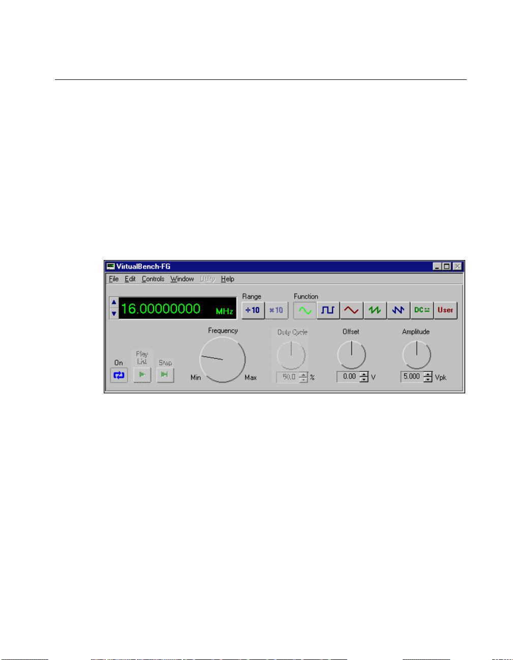
Generating Standard Functions
If you need to generate standard waveforms such as a sine, square, ramp,
or DC signal, you can use the VirtualBench-FG soft front panel shown in
Figure 1-6. Launch the front panel by selecting Start»Programs»National
Instruments FGEN»VirtualBench FG. You use this front panel to
control the frequency, amplitude, offset, and type of waveform generated.
The maximum sine frequency you can generate is 16 MHz. The maximum
amplitude is 5 V
the actual levels will be twice that shown on the front panel.
into a 50 Ω load. If the load is a high-impedance load,
pk
Figure 1-6.
©
National Instruments Corporation 1-11 NI 5401 User Manual
VirtualBench-FG Soft Front Panel for Function Generation
Page 19

Chapter 1 Generating Functions with the NI 5401
To control additional instrument parameters, select Edit»54xx Settings to
bring up the dialog box shown in Figures 1-7 and 1-8.
Figure 1-7. VirtualBench-FG General Settings Dialog Box for the NI 5401
Figure 1-8. VirtualBench-FG Signals Settings Dialog Box for the NI 5401
Note Refer to the online help for further information about the 54xx Settings dialog box.
NI 5401 User Manual 1-12 www.natinst.com
Page 20

Chapter 1 Generating Functions with the NI 5401
You can also load a custom waveform pattern with VirtualBench-FG. This
waveform should be a text file and should contain exactly 16,384 samples.
If the defined waveform does not contain exactly 16,384 samples, you may
see undesired effects in your wa veform output. F ollow these steps to load a
custom waveform:
1. Select File»Load Waveform to bring up the dialog box shown in
Figure 1-9.
Figure 1-9. VirtualBench-FG Load Waveform Dialog Box
2. Specify the delimiter used in the text file, the number of columns, the
start line, and the number of samples.
3. Click OK to return to the main VirtualBench-FG screen shown in
Figure 1-6.
4. Click the User button to use the information in the text file as the
source for the waveform.
5. Click the On button to generate the waveform.
Generating Multiple Frequencies in a Sequence
If desired, you can generate multiple frequencies in a sequence, which can
include frequency sweeping, hopping, and so on. You can list up to 512
different frequencies and specify the duration of generation for each of
©
National Instruments Corporation 1-13 NI 5401 User Manual
Page 21

Chapter 1 Generating Functions with the NI 5401
them using the VirtualBench-FG Frequency List Editor. Follow these steps
to create a list of multiple frequencies:
1. Select Window»Frequency List Editor from the VirtualBench-FG
soft front panel to bring up the dialog box shown in Figure 1-10.
Figure 1-10. VirtualBench-FG Frequency List Editor Dialog Box
2. Specify the frequency and duration of each function in the sequence.
3. Save the sequence by selecting File»Save.
4. To return to the main VirtualBench-FG screen shown in Figure 1-6,
select File»Close.
5. Select File»Load Frequency List to load the frequency list.
Y ou can combine the frequency list generation with diff erent trigger modes
to get the desired frequency generation.
NI 5401 User Manual 1-14 www.natinst.com
Page 22

Waveform Editor
Chapter 1 Generating Functions with the NI 5401
You can use the Waveform Editor shown in Figure 1-11 to create a custom
waveform. To launch the Waveform Editor, select Start»Programs»
National Instruments FGEN»Waveform Editor. You can select
waveforms from the function library, write equations, or draw them
manually. Each segment can have more than one waveform component in
it, and you can perform a variety of math functions on each component.
Figure 1-11.
Waveform Editor Soft Front Panel
This soft front panel is resizable so you can view the w av eforms you create
with as much precision as you wish. You can save the waveforms in the
following formats:
• Voltage (
•Text (
• Binary (
.wfm)
.txt)
.bin)
T ext wav eforms are the only format you can use with the NI 5401, and they
must contain exactly 16,384 samples to function properly.
©
National Instruments Corporation 1-15 NI 5401 User Manual
Page 23

Chapter 1 Generating Functions with the NI 5401
Power-Up and Reset Conditions
When you power up your computer, the NI 5401 is in the following state:
• The output is disabled and set to 0 V.
• The trigger mode is set to continuous.
• The trigger source is set to automatic (the software provides the
triggers).
• The digital filter is enabled.
• Output attenuation remains unchanged from its previous setting.
• The analog filter remains unchanged from its previous setting.
• Output impedance remains unchanged from its previous setting.
When you reset the board using NI-FGEN or any other application
software, your NI 5401 is in the same state as shown at power up,
previously listed, with the following differences:
• Output attenuation is set to 0 dB.
• The analog filter is enabled.
• Output impedance is set to 50 Ω.
• The PLL reference source is set to internal tuning.
• The SYNC duty cycle is set to 50%.
NI 5401 User Manual 1-16 www.natinst.com
Page 24

Function Generator Operation
This chapter describes how to use your NI 5401.
Figure 2-1 shows the NI 5401 block diagram.
RTSI/PXI Trigger Bus
2
Instruction
FIFOs
IFIFO
Control
Clock
Controls
Filter
Controls
Data Path
Bus
Interface
RTSI
Control
Waveform
Sequencer
Trigger
Control
DDS +
Lookup
Memory
DDS
Control
Analog
Control
Digital
Filter
PXI/PCI Channel
Figure 2-1.
Attenuators,
DAC
NI 5401 Block Diagram
Filter, and
Amplifier
Level
Crossing
Detector
PLL and
Clocking
ARB
SYNC
PLL Ref
©
National Instruments Corporation 2-1 NI 5401 User Manual
Page 25

Chapter 2 Function Generator Operation
The NI 5401 has several main components:
• A PXI or PCI bus interface that handles Plug and Play protocols for
assigning resources to the device and providing drivers for the data and
address bus that are local to the device
• A waveform sequencer that performs multiple functions such as
arbitrating the data buses and controlling the triggers, filters,
attenuators, clocks, PLL, RTSI switch, instruction FIFO, and DDS
• The data from the memory is fed to a digital-to-analog converter
(DA C) through a half-band interpolating digital filter . The output from
the DAC goes through the filter to the amplifiers, attenuators, and,
finally, the I/O connector.
Generating Waveforms
The NI 5401 generates waveforms using DDS, which is used for generating
standard waveforms that are repetitive in nature, such as sine, TTL, square,
and triangular waveforms. DDS mode limits you to one buffer, and the
buffer size must be exactly equal to 16,384 samples.
Figure 2-2 shows a block diagram of the data path for waveform
generation. The data for waveform generation comes from DDS lookup
memory. This data is interpolated by a half-band digital filter and then fed
to a high-speed DAC. The data has a pipeline delay of 26 update clocks
through this digital filter. Although the digital filter can be disabled through
software, there will still be a 26 update clock delay.
A
12 Bits
Digital Filter
DDS Lookup
Memory
Digital Filter
Enable
DDS
Figure 2-2.
Filter
12
MUX
B
Div/2
Waveform Data Path Block Diagram
DAC Register
80 MHz Oscillator
DAC12
On the NI 5401, the high-speed DAC is always updated at 80 MHz, but the
update clock for memory is 40 MHz.
NI 5401 User Manual 2-2 www.natinst.com
Page 26

Direct Digital Synthesis (DDS)
Direct digital synthesis (DDS) is a technique for deriving, under digital
control, an analog frequency source from a single reference clock
frequency. This technique produces high-frequency accuracy and
resolution, temperature stability, wideband tuning, and rapid and
phase-continuous frequency switching.
The NI 5401 uses a 32-bit, high-speed accumulator with a lookup memory
and a 12-bit DAC for DDS-based waveform generation. Figure 2-3 shows
the building blocks for DDS-based waveform generation.
Chapter 2 Function Generator Operation
Frequency
Time
Frequency
Time
Instruction FIFO
DDS
Sequencer
16-Bit
Counter
(14)
Lookup
Memory
Div/2
Figure 2-3.
Data Out (16)
80 MHz Oscillator
DDS Building Blocks
The lookup memory is dedicated to the DDS. Y ou can store one cycle of a
repetitive waveform—a sine, triangular, square, or arbitrary wave—in the
lookup memory . Then, you can change the frequency of that waveform by
sending just one instruction. You can use DDS mode for very fine
frequency resolution function generation. You can generate sine waves of
up to 16 MHz with the NI 5401. Waveform generation always loops back
to the beginning of the lookup memory after passing through the end of the
lookup memory.
The NI 5401 uses a lookup waveform memory for storing the waveform
buffer and FIFO memory for storing the staging list, which contains
multiple frequency list information. This FIFO is referred to as an
instruction FIFO.
©
National Instruments Corporation 2-3 NI 5401 User Manual
Page 27

Chapter 2 Function Generator Operation
Each stage is made up of two instructions: the frequency, which specifies
the frequency of the waveform to be generated, and the time, which
specifies the time for which the frequency is to be generated.
Note You cannot specify the number of iterations for a waveform to be generated.
Frequency Hopping and Sweeping
You can define a staging list for performing frequency hops and sweeps.
The entire staging list uses the same buffer loaded into the lookup memory.
All stages differ in the frequency to be generated.
Note The minimum time that a frequency should be generated is 2 µs. Therefore, the
maximum hop rate from frequency to frequency is 500 kHz.
The maximum number of stages that can be stored in the instruction FIFO
for DDS mode is 512. For more information on the waveform generation
process, refer to your software documentation.
Triggering
You use triggering to start and step through a waveform generation. The
trigger sources and modes of operation are explained in the following
sections.
Trigger Sources
Trigger sources are software selectable. By default, the software produces
the trigger sources. You can also use an external trigger from a pin on the
digital I/O connector, the RTSI trigger lines on the RTSI bus, or the TTL
trigger lines on the PXI trigger bus on the backplane. Figure 2-4 shows the
trigger sources for the NI 5401.
NI 5401 User Manual 2-4 www.natinst.com
Page 28

RTSI/PXI Trigger
Chapter 2 Function Generator Operation
RTSI/PXI Trigger
Lines <0..6>
7
RTSI Switch
Modes of Operation
External Trigger
Software Trigger
Trigger Select
Figure 2-4. Waveform Generation Trigger Sources
Digital
MUX
Start Trigger
If you need to automatically trigger the waveform generation, use software
to generate the triggers. A rising TTL edge is required for external
triggering. For more information on triggering over RTSI lines, see the
RTSI/PXI Trigger Lines section later in this chapter.
The NI 5401 has three triggering modes—single, continuous, and
stepped—described in the following sections.
Single Trigger Mode
The waveform you define in the staging list is generated only once by going
through the entire staging list. Only one trigger is required to start the
waveform generation.
In single trigger mode, after the NI 5401 receives a trigger, the waveform
generation starts at the first stage and continues through the last stage. The
last stage is generated repeatedly until you stop the waveform generation.
Figure 2-5 illustrates a single trigger mode of operation.
©
National Instruments Corporation 2-5 NI 5401 User Manual
Page 29

Chapter 2 Function Generator Operation
Start Trigger
f1, ∆T1
End of All Stages
f2, ∆T2
f3, ∆T3
Last Stage Generated
f4
Continuously Until Stopped
Figure 2-5. Single Trigger Mode
For example, assume that one cycle of a sine wave is stored in the DDS
lookup memory. F or stage 1, f1 specifies the sine frequency to be generated
for time ∆T1, f2 and ∆T2 for stage 2, and so on. If there are four stages in
the staging list, f4 will be generated continuously until the waveform
generation is stopped.
Continuous Trigger Mode
The waveform you define in the staging list is generated infinitely by
continually cycling through the staging list. After a trigger is received, the
waveform generation starts at the first stage, continues through the last
stage, and loops back to the start of the first stage, continuing until you stop
the waveform generation. Only one trigger is required to start the waveform
generation.
Figure 2-6 illustrates a continuous trigger mode of operation.
Start Trigger
(f1, ∆T1)
End of All Stages
(f2, ∆T2)
(f3, ∆T3)
(f4, ∆T4)
(f1, ∆T1)
Repeat
Until Stopped
(f2, ∆T2)
Figure 2-6. Continuous Trigger Mode
NI 5401 User Manual 2-6 www.natinst.com
Page 30

Chapter 2 Function Generator Operation
Stepped Trigger Mode
After a start trigger is received, the waveform defined by the first stage is
generated. Then, the device waits for the next trigger signal. On the next
trigger, the waveform described by the second stage is generated, and so on.
Once the staging list is exhausted, the waveform generation returns to the
first stage and continues in a cyclic fashion.
Figure2-7 illustrates a stepped trigger mode of operation. Switching from
stage to stage is phase continuous. In this mode, the time instruction is not
used. The trigger paces the waveform generation from one frequency to the
other.
Start Trigger
f1 f2
Analog Output
Note
The DAC output can be fine-tuned for gain and offset. Since the offset is adjusted
before the main attenuators and amplifier, it is referred to as pre-attenuation offset. This
fine-tuning of gain and offset is performed by separate DACs.
Start Trigger
Start Trigger
Start Trigger
f3
End of All Stages
Figure 2-7.
Stepped Trigger Mode
f4
Start Trigger
f1
Analog waveforms are generated as follows:
1. The 12-bit digital waveform data is fed to a high-speed DAC.
2. A lowpass filter filters the DAC output.
3. This filtered signal is amplified before it goes to a 10 dB attenuator.
4. The output from the 10 dB attenuator then goes to the main amplifier,
which can provide up to ±5 V levels into 50 Ω. An output relay can
switch between ground level and the main amplifier. Refer to the
Output Enable section of this document for additional information
about this relay.
5. The output of this relay goes to a series of passive attenuators.
6. The output of the attenuators goes through a selectable output
impedance of 50or75Ω to the I/O connector.
©
National Instruments Corporation 2-7 NI 5401 User Manual
Page 31

Chapter 2 Function Generator Operation
Figure 2-8 shows the essential block diagram of analog waveform
generation.
12
Clock
DAC
Lowpass
Filter
Gain
DAC
Offset
DAC
Level
DAC
Pre Amp
10 dB
Attenuator
Main Amp
Comparator
+
-
Output
Enable
50 Ω
Attenuators
(63 dB in 1 dB steps)
50 Ω
25 Ω
50 Ω/75 Ω
Selector
Figure 2-8. Analog Output and SYNC Out Block Diagram
Figure 2-9 shows the timing relationships of the trigger input and
waveform output. T
is the pulse width on the trigger signal. Td2 is the time
d1
delay from trigger to output on Arb output. Refer to Appendix A,
Specifications, for more information on these timing parameters.
Arb
SYNC
T
d1
Trigger Input Signal
(Slope: Positive, TTL)
Waveform Output
(±5 V
into 50 Ω
pp
)
T
d2
Figure 2-9. Waveform and Trigger Timings
Note
Y ou can switch off the analog lo wpass filter at any time during wav eform generation.
When you change this setting, the bouncing of electromechanical relays on the NI 5401
distorts the output signal for about 10 ms.
NI 5401 User Manual 2-8 www.natinst.com
Page 32

SYNC Output and Duty Cycle
The SYNC output is a TTL version of the sine waveform generated at the
output. The signal from the pre-amplifier is sent to a comparator, where it
is compared against a level set by the level DAC. The output of this
comparator is sent to the SYNC connector through a hysteresis buffer and
a 50 Ω series resistor to reverse terminate reflected pulses.
You can use the SYNC output as a very high-frequency resolution,
software-programmable clock source for many applications. You also can
vary the duty cycle of SYNC output, on the fly, by changing the output of
the level DAC. The SYNC output might not carry meaning for other types
of generated waveforms.
Note
You can change the duty cycle of the SYNC output at any time during waveform
generation.
Output Attenuation
Figure2-10 shows the NI5401 output attenuator chain. The output
attenuators are made of resistor networks and may be switched in any
combination. The maximum attenuation possible on the NI5401 is 73 dB.
Chapter 2 Function Generator Operation
1 dB
In
2 dB 4 dB
8 dB
Figure 2-10.
16 dB
Output Attenuation Chain
32 dB
Out
By attenuating the output signal, you keep the dynamic range of the DAC;
that is, you do not lose any bits from the digital representation of the signal
because the attenuation is done after the DAC and not beforeit.
attenuation (in decibels) = –20 log
whereV
Note
For the NI5401, Vi = ±5 V for a terminated load and ±10 V for an
= desired voltage level for the output signal
o
V
= input voltage level.
i
(Vo /Vi)
10
unterminatedload.
©
National Instruments Corporation 2-9 NI 5401 User Manual
Page 33

Chapter 2 Function Generator Operation
NI-FGEN calculates the value of the output attenuation chain, which you
can control by changing the peak-to-peak amplitude parameter. 0dB
attenuation corresponds to an amplitude of 10V
attenuation of 73dB corresponds to an amplitude of 2.24mV
amplitude less then this is coerced to this value.
Note You can change the output attenuation at any time during waveform generation.
When you change this setting, the bouncing of electromechanical relays on the NI5401
distorts the output signal for about 10 ms.
Output Impedance
As shown in Figure2-10, before the signal reaches the output connector,
you can select an output impedance of 50Ω or 75Ω. If the load impedance
is 50Ω and all the attenuators are off (an output attenuation of 0dB), the
output levels are ±5 V.
Most applications use a load impedance of 50Ω, but applications such as
video device testers require 75Ω. If the load is a very high-input impedance
load (~1 MΩ), you will see output levels up to ±10V.
Note You can change the output impedance at any time during waveform generation.
When you change this setting, the bouncing of electromechanical relays on the NI5401
distorts the output signal for about 10ms.
. The maximum
pk-pk
pk-pk
. Any
Output Enable
You can switch off the waveform generation at the output connector by
controlling the output enable relay, as shown in Figure2-8. When the
output enable relay is off, the output signal level goes to ground level.
Note Even though the output enable relay is in the off position, the waveform generation
process continues internally on the NI5401.
You can use this feature to disconnect and connect different devices to the
NI5401 on the fly.
Note You can change the output enable state at any time during waveform generation.
When you change this setting, the bouncing of electromechanical relays on the NI5401
distorts the output signal for about 10ms.
NI 5401 User Manual 2-10 www.natinst.com
Page 34

Chapter 2 Function Generator Operation
Pre-Attenuation Offset
The NI 5401 hardware supports a DC offset of up to ±2.5 V before the
attenuation chain. Unless the 10 dB attenuator is switched in, which occurs
when the amplitude is less then 3.16 V
, the waveform maximum plus
pk-pk
the offset must not exceed ±5 V into 50 Ω. If it does, the waveform is
clipped. Refer to Figure 2-8 for a diagram showing the location of the
10 dB attenuator.
NI-FGEN automatically calculates the pre-attenuation offset value based
on the DC offset and amplitude values, so the allowable DC offset range is
dependent on the amplitude. For example, if you have an amplitude of
1V
, the maximum DC offset you can apply is 0.25 V, which
pk-pk
corresponds to a pre-attenuation offset of 2.5 V.
Note
You can change the DC Offset at any time during waveform generation. Refer to
your software documentation for additional information.
Phase-Locked Loops and Board Synchronization
Figure 2-11 illustrates the block diagram for the NI 5401 for PCI PLL
circuit. Figure 2-12 illustrates the block diagram for the NI 5401 for PXI
PLL circuit. The PLL consists of a voltage-controlled crystal oscillator
(VCXO) with a tuning range of ±100 ppm. This VCXO generates the main
clock of 80 MHz.
The PLL can lock to a reference clock source from the external connector ,
from a RTSI Osc line on the RTSI bus (NI 5401 for PCI) , or fro m a
10 MHz Osc line on the PXI backplane bus (for NI 5401 for PXI). The PLL
can also be tuned internally using a calibration DAC (CalDAC). National
Instruments accurately performs this tuning during manufacturing. Refer to
the RTSI/PXI Trigger Lines section later in this manual for additional
information on using the RTSI and 10 MHz Osc lines.
The reference and VCXO clock are compared by a phase comparator
running at 1 MHz. The loop filters the error signal and sends it to the control
pin of the VCXO to complete the loop.
©
National Instruments Corporation 2-11 NI 5401 User Manual
Page 35

Chapter 2 Function Generator Operation
Board Clock (Master)
Master/Slave
RTSI Clock (Slave)
Source
Loop
Filter
RTSI
Switch
(20 MHz)
Phase
Comp
RTSI Osc
RTSI Bus
Control
Voltage
VCXO
Source
Control
Voltage
VCXO
AMUX
80 MHz
Div/4
Tune
DAC
20 MHz
14
(1 V
Board Clock
Figure 2-11. PLL Architecture for the NI 5401 for PCI
10 MHz Osc
80 MHz
AMUX
Div/8
Loop
Filter
CAL
DAC
10 MHz
Phase
Comp
(1 V
Figure 2-12. PLL Architecture for the NI 5401 for PXI
PLL Ref
pk-pk
PXI Bus
PLL Ref
pk-pk
min)
min)
Y ou can frequenc y lock to an external reference clock source of 1 MHz and
from 5–20 MHz in 1 MHz increments. The PLL can lock to a signal level
of at least 1 V
Caution Do not increase the voltage level of the clock signal at the PLL reference input
connector by more than the specified limit, 5 V
Note If two or more NI 5401 devices are locked to each other using the same reference
pk-pk
.
.
pk-pk
clock, they are frequency locked, but the phase relationship is indeterminate.
NI 5401 User Manual 2-12 www.natinst.com
Page 36

Analog Filter Correction
The NI5401 can correct for slight deviations in the flatness of the
frequency characteristic of the analog lowpass filter in its passband, as
shown in Figure2-13. Curve A shows a typical lowpass filter curve. The
response of the filter is stored in an onboard EEPROM in 1 MHz
increments up to 16 MHz. CurveC is the correction applied to the
frequency response. The resulting CurveB is a flat response over the entire
passband. If you want to generate a sine wave at a particular frequency with
filter correction applied, you have to specify that frequency through your
software.
Gain (dB)
Chapter 2 Function Generator Operation
A
B
C
Frequency (MHz)
A. Typical Analog Filter Characteristics
B. Corrected Filter Characteristics
C. Correction Applied
Figure 2-13.
Note
You can change the filter frequency correction at any time during waveform
Analog Filter Correction
generation.
©
National Instruments Corporation 2-13 NI 5401 User Manual
Page 37

Chapter 2 Function Generator Operation
RTSI/PXI Trigger Lines
The NI 5401 for PCI contains seven trigger lines and one RTSI clock line
available over the RTSI bus to send and receive NI 5401-specific
information to other boards that have RTSI connectors. Figure 2-14 shows
the RTSI trigger lines and routing of NI 5401 for PCI signals to the RTSI
switch.
SYNC
Start Trigger
RTSI Trigger
Board Clock
Master/Slave
RTSI Clock
Figure 2-14.
RTSI
Switch
RTSI Trigger Lines and Routing for the NI 5401 for PCI
RTSI 0
RTSI 1
RTSI 2
RTSI 3
RTSI 4
RTSI 5
RTSI 6
RTSI Osc
RTSI Bus
Figure 2-15 shows the PXI trigger lines and routing of NI 5401 for PXI
signals to the RTSI switch.
SYNC
Start Trigger
RTSI Trigger
BOARD_SYNC
RTSI
Switch
TRIG 0
TRIG 1
TRIG 2
TRIG 3
TRIG 4
TRIG 5
PXI STAR
PXI Bus
PXI 10MHz Osc
Figure 2-15.
PXI Trigger Lines, 10 MHz Backplane Oscillator, and Routing for the
NI 5401 for PXI
NI 5401 User Manual 2-14 www.natinst.com
Page 38

Chapter 2 Function Generator Operation
The NI 5401 can receive a hardware trigger from another board as a RTSI
trigger signal on any of the RTSI/PXI trigger lines.
You can also route signals as follows:
• Route the Start Trigger signal generated on the NI 5401 to other boards
through any of the RTSI/PXI bus trigger lines.
• Route the SYNC output generated on the NI 5401 to other boards
through any of the RTSI/PXI b u s trigger lines.You can use this signal
to give other boards an accurate and fine frequency resolution clock.
♦ NI 5401 for PCI
For frequency locking to other boards as a master, the NI 5401 sends an
onboard 20 MHz signal to the RTSI Osc line as a board clock signal. For
locking to other devices as a slave, the NI 5401 receives the RTSI Osc line
as a RTSI clock signal.
♦ NI 5401 for PXI
For frequency locking to other boards, the NI 5401 for PXI receives the
PXI backplane 10 MHz Osc as a reference clock signal. All the NI 5401s
for PXI use this common signal as the reference clock for frequency
locking.
Note Refer to your software documentation for selecting and routing signals to the
RTSI/PXI trigger bus.
Calibration
Calibration is the process of minimizing measurement errors by making
small circuit adjustments. On the NI 5401, NI-FGEN automatically makes
these adjustments by retrieving predetermined constants from the onboard
EEPROM, calculating correction values, and writing those values to the
CalDACs.
National Instruments calibrates all NI 5401 devices to the levels indicated
in Appendix A, Specifications. Factory calibration involves procedures
such as nulling the offset and gain errors. However, since offset and gain
errors may drift with time and temperature, you may need to recalibrate
your device. Contact National Instruments to recalibrate your NI 5401.
©
National Instruments Corporation 2-15 NI 5401 User Manual
Page 39

Specifications
This appendix lists the specifications for the NI 5401. These specifications
are typical at 25 °C unless otherwise stated. The operating temperature
range is 0 to 50 °C.
Analog Output
Number of channels...............................1
Resolution ..............................................12 bits
Maximum update rate ............................40 MHz
DDS accumulator................................... 32 bits
Frequency range
Sine .................................................16 MHz, max
SYNC (TTL)...................................16 MHz, max
Square .............................................1 MHz, max
Ramp............................................... 1 MHz, max
Triangle...........................................1 MHz, max
A
Frequency resolution ..............................9.31 mHz
Voltage Output
Ranges
.....................................................±5 V into a 50 Ω load
±10 V into a high-impedance load
Accuracy ................................................±0.1 dB
Output attenuation..................................0 to 73 dB
Resolution....................................... 0.001 dB steps
©
National Instruments Corporation A-1 NI 5401 User Manual
Page 40

Appendix A Specifications
Pre-attenuation offset
Range...............................................±2.5 V into 50 Ω
1
Accuracy..........................................±5 mV
Output coupling .....................................DC
Output impedance ..................................50 Ω or 75 Ω software selectable
Load impedance .....................................50 Ω or greater
Output enable..........................................Software switchable
Protection................................................Short-circuit protected
Sine Spectral Purity
Harmonic products and spurs
Up to 1 MHz....................................–60 dBc
Up to 16 MHz..................................–35 dBc
Phase noise .............................................–105 dBc/Hz at 10 kHz from
carrier
Filter Characteristics
Digital
Type.................................................Half-band interpolating
Selection..........................................Software switchable (enable or
disable)
Taps ................................................67
Filter coefficients ............................Fixed 20-bit
Data interpolating frequency ..........80 MS/s
Pipeline signal delay .......................26 sampling periods
Analog
Type.................................................7th-order L-C lowpass filter
Passband ripple................................±2 dB
1
With less than 10 dB of attenuation, signal maximum plus offset (before attenuation) must not exceed ±5 V (into 50
NI 5401 User Manual A-2 www.natinst.com
Ω)
Page 41

Triggers
Appendix A Specifications
Waveform Specifications
Memory.................................................. 16,384 16-bit samples
Segment length.......................................16,384 samples, exact
Segment linking (instruction FIFO)....... 512 links
Timing I/O
Update clock ..........................................Internal, 40 MHz only
Frequency locking
External reference sources.............. Input connector, RTSI clock line,
or internal
Reference clock frequencies........... 1 MHz, 5–20 MHz in 1 MHz steps
Frequency locking range.................±100 ppm
Digital Trigger
Compatibility ........................................ TTL
Response ...............................................Rising edge
Pulse width (T
Trigger to waveform
output delay (T
)....................................20 ns min
d1
)...................................28 sample clocks + 150 ns max
d2
RTSI
Trigger lines ..........................................7
Clock lines..............................................1
Bus Interface
Type .......................................................Slave
Operational Modes
Type .......................................................Single, continuous, stepped
©
National Instruments Corporation A-3 NI 5401 User Manual
Page 42

Appendix A Specifications
SYNC Out
Level ......................................................TTL
Duty cycle...............................................20% to 80%, software
External Clock Reference Input
Frequency ...............................................1 MHz or 5–20 MHz in 1 MHz
controllable
steps
Internal Clock
Mechanical
Amplitude...............................................1 V
Frequency ...............................................40 MHz
Initial accuracy .......................................±5 ppm
Temperature stability (0 to 5 °C)............±25 ppm
Aging (1 year).........................................±5 ppm
Connectors
ARB (output)...................................SMB/BNC
SYNC (output).................................SMB/BNC
PLL reference (input)......................SMB
External trigger in............................50-pin digital (PCI),
SMB (PXI)
Size .........................................................1 slot
Power requirements ...............................5 V, 3.5 A max
12 V, 125 mA
≤ level ≤ 5 V
pk-pk
pk-pk
NI 5401 User Manual A-4 www.natinst.com
Page 43

Optional Accessories
National Instruments offers a variety of products to use with your NI 5401,
including probes, cables, and other accessories:
• Shielded and unshielded I/O connector blocks (SCB-68, TBX-68,
CB-68)
• RTSI bus cables
For more specific information about these products, refer to your National
Instruments catalogue or Web site, or call the office nearest you.
Cabling
The following list gives recommended part numbers for cables that you can
use with your NI 5401 device:
• BNC male to BNC male, 50 Ω cable from ITT Pomona Electronics
(part number BNC-C-xx)
• BNC male to BNC male, 75 Ω cable from ITT Pomona Electronics
(part number 2249-E-xx)
• BNC female to RCA phono plug adapter, from ITT Pomona
Electronics (part number 5319)
• BNC 50 Ω feed-through terminator adapter from ITT Pomona
Electronics (part number 4119-50)
• BNC female-female adapter from ITT Pomona Electronics
(part number 3283)
B
©
National Instruments Corporation B-1 NI 5401 User Manual
Page 44

Frequency Resolution and
Lookup Memory
For DDS-based waveform generation, you must first load one cycle of the
desired waveform into the lookup memory. The size of the DDS lookup
memory is 16,384 samples. Each sample is 16 bits wide.
Note
One cycle of the waveform buffer loaded into the memory should be exactly equal
to the size of the DDS lookup memory.
= update clock for the accumulator.
F
c
C
For the NI 5401, F
F
= desired frequency of the output signal
a
N = accumulator size in bits
For the NI 5401, N = 32.
FCW = frequency control word to be loaded into the accumulator to
generate F
The frequency control word is calculated using the formula:
FCW = (2
The frequency resolution is then given by:
frequency resolution = F
For example, if you need to generate a frequency of 10 MHz, then the FCW
32
is (2
* 10E6)/40E6, which equals 1,073,741,824. If you need to generate
a frequency of 1 Hz, then the FCW is (2
Note
On the NI 5401, the maximum frequency of a sine wave you can generate reliably
is limited to 16 MHz. Other waveforms such as square or triangular waves are limited to
1MHz.
= 40 MHz.
c
.
a
N
* Fa) / F
c
/ 2N = (40 × 106) / 232 = 9.31322 mHz
c
32
* 1)/40E6, which equals 107.
©
National Instruments Corporation C-1 NI 5401 User Manual
Page 45

Appendix C Frequency Resolution and Lookup Memory
You can also synthesize arbitrary waveforms using DDS. Generating
arbitrary waveforms this way will be very limited; you are restricted to a
single buffer, and this buffer should be exactly equal to the size of the
lookup memory (16,384 samples).
T o update e v ery sample of an arbitrary w av eform in lookup memory at the
maximum clock rate of 40 MHz, the software writes an FCW value of
(N–L)
2
, where N is the size of the accumulator and L is the number of
address bits of lookup memory (L = 14 bits). Thus, the FCW value for the
NI 5401 equals 262,144. Since FCW = (2
so you would write a frequency value of (2
equals 2.441 kHz
If you want to update every sample in lookup memory at an integral
subdivision, D, of the maximum clock rate, then you want an FCW value
(N–L–D+1)
of 2
. In other words, for an effectiv e update rate of ev ery sample at
half the maximum clock rate, write a frequency value of
(32–14–2+1)
(2
×(40 × 106)) / 232, which equals 1.221 kHz.
N
* Fa) / Fc, Fa=(2
(32–14)
×(40 × 106)) / 232, which
(N–L)
*Fc)/2N,
NI 5401 User Manual C-2 www.natinst.com
Page 46

Technical Support Resources
This appendix describes the comprehensive resources available to you in
the Technical Support section of the National Instruments Web site and
provides technical support telephone numbers for you to use if you have
trouble connecting to our Web site or if you do not have internet access.
NI Web Support
To provide you with immediate answers and solutions 24 hours a day,
365 days a year, National Instruments maintains extensi ve online technical
support resources. They are available to you at no cost, are updated daily,
and can be found in the Technical Support section of our Web site at
www.natinst.com/support.
On-Line Problem-Solving and Diagnostic Resources
• KnowledgeBase—A searchable database containing thousands of
frequently asked questions (FA Qs) and their corresponding answers or
solutions, including special sections devoted to our newest products.
The database is updated daily in response to new customer experiences
and feedback.
• Troubleshooting Wizards—Step-by-step guides lead you through
common problems and answer questions about our entire product line.
Wizards include screen shots that illustrate the steps being described
and provide detailed information ranging from simple getting started
instructions to advanced topics.
• Product Manuals—A comprehensive, searchable library of the latest
editions of National Instruments hardware and software product
manuals.
• Hardware Reference Database—A searchable database containing
brief hardware descriptions, mechanical drawings, and helpful images
of jumper settings and connector pinouts.
• Application Notes—A library with more than 100 short papers
addressing specific topics such as creating and calling DLLs,
developing your own instrument driver software, and porting
applications between platforms and operating systems.
D
©
National Instruments Corporation D-1 NI 5401 User Manual
Page 47

Appendix D Technical Support Resources
Software-Related Resources
• Instrument Driver Network—A library with hundreds of instrument
drivers for control of standalone instruments via GPIB, VXI, or serial
interfaces. You also can submit a request for a particular instrument
driver if it does not already appear in the library.
• Example Programs Database—A database with numerous,
non-shipping example programs for National Instruments
programming environments. You can use them to complement the
example programs that are already included with National Instruments
products.
• Software Library—A library with updates and patches to application
software, links to the latest versions of driver software for National
Instruments hardware products, and utility routines.
Worldwide Support
National Instruments has offices located around the globe. Many branch
offices maintain a Web site to provide information on local services. You
can access these Web sites from
www.natinst.com/worldwide.
If you have trouble connecting to our Web site, please contact your local
National Instruments office or the source from which you purchased your
National Instruments product(s) to obtain support.
For telephone support in the United States, dial 512 795 8248. For
telephone support outside the United States, contact your local branch
office:
Australia 03 9879 5166, Austria 0662 45 79 90 0, Belgium 02 757 00 2 0,
Brazil 011 284 5011, Canada (Ontario) 905 785 0085,
Canada (Québec) 514 694 8521, China 0755 3904939,
Denmark 45 76 26 00, Finland 09 725 725 11, France 01 48 14 24 24,
Germany 089 741 31 30, Hong Kong 2645 3186, India 91805275406,
Israel 03 6120092, Italy 02 413091, Japan 03 5472 2 970,
Korea 02 596 7456, Mexico (D.F.) 5 280 7625,
Mexico (Monterrey) 8 357 7695, Netherlands 0348 433466,
Norway 32 27 73 00, Singapore 22658 86, Spain (Madrid) 91 640 0085,
Spain (Barcelona) 93 582 0251, Sweden 08 587 895 00,
Switzerland 056 200 51 51, Taiwan 02 2377 1200,
United Kingdom 01635 523545
NI 5401 User Manual D-2 www.natinst.com
Page 48

Glossary
Prefix Meaning Value
µ- micro- 10
m- milli- 10
k- kilo- 10
M- mega- 10
Numbers/Symbols
% percent
+ positive of, or plus
– negative of, or minus
± plus or minus
/per
–6
–3
3
6
°degree
Ω ohm
+5 V +5 V output signal
A
A amperes
amplification method of scaling the signal level to a higher level
ARB normal waveform output signal
attenuation decreasing the amplitude of a signal
©
National Instruments Corporation G-1 NI 5401 User Manual
Page 49

Glossary
B
b bit—one binary digit, either 0 or 1
B byte—eight related bits of data, an eight-bit binary number. Also used to
denote the amount of memory required to store one byte of data.
BNC a type of coaxial signal connector
buffer temporary storage for acquired or generated data
bus the group of conductors that interconnect individual circuitry in a computer.
Typically, a bus is the expansion vehicle to which I/O or other devices are
connected. Examples of PC buses are the AT bus (also known as the ISA
bus) and the PCI bus.
C
C Celsius
CalDAC calibration DAC
clock hardware component that controls timing for reading from or writing to
groups
CMOS complementary metal-oxide semiconductor
continuous trigger mode repeats a staging list until waveform generation is stopped
counter a circuit that counts external pulses or clock pulses (timing)
coupling the manner in which a signal is connected from one location to another
D
DAC digital-to-analog converter—an electronic device, often an integrated
circuit, that converts a digital number into a corresponding analog voltage
or current
dB decibel—the unit for expressing a logarithmic measure of the ratio of two
signal levels: dB = 20 log
dBc decibel referred to carrier level
NI 5401 User Manual G-2 www.natinst.com
V1/V2, for signals in volts
10
Page 50

Glossary
DC direct current
DC coupled allowing the transmission of both AC and DC signals
DDS direct digital synthesis—a digital technique of frequency generation using
a numerically controlled oscillator (NCO), a dedicated lookup memory,
and a DAC
DDS mode a method of waveform generation that uses built-in DDS functionality to
generate very high frequency resolution standard waveforms
DGND digital ground signal
digital word See word.
driver software that controls a specific hardware device
dynamic range the ratio of the largest signal lev el a circuit can handle to the smallest signal
level it can handle (usually taken to be the noise level), normally expressed
in dB
E
EEPROM electrically erasable programmable read-only memory—ROM that can be
erased with an electrical signal and reprogrammed
external trigger a voltage pulse from an external source that triggers an event such as A/D
conversion
EXT_TRIG external trigger input signal
©
National Instruments Corporation G-3 NI 5401 User Manual
Page 51

Glossary
F
FIFO first-in first-out memory buf fer—the first data stored is the f irst data sent to
the acceptor. FIFOs are often used on DAQ devices to temporarily store
incoming or outgoing data until that data can be retrieved or output. For
example, an analog input FIFO stores the results of A/D conversions until
the data can be retrieved into system memory, a process that requires the
servicing of interrupts and often the programming of the DMA controller.
This process can take several milliseconds in some cases. During this time,
data accumulates in the FIFO for future retrieval. With a larger FIFO,
longer latencies can be tolerated. In the case of analog output, a FIFO
permits faster update rates, because the waveform data can be stored on the
FIFO ahead of time. This again reduces the effect of latencies associated
with getting the data from system memory to the DAQ device.
filters digital or analog circuits that change the frequency characteristics of a
waveform
frequency hop change from one frequency to another
frequency resolution the smallest frequency change that can be generated by a NI 5411/5431
frequency sweep change the frequency of a waveform in a controlled manner
G
gain the factor by which a signal is amplified, sometimes expressed in decibels
GUI graphical user interface
H
hardware the physical components of a computer system, such as the circuit boards,
plug-in boards, chassis, enclosures, peripherals, cables, and so on
HiZ high impedance
Hz hertz—the number of cycles or repetitions per second
NI 5401 User Manual G-4 www.natinst.com
Page 52

Glossary
I
I/O input/output—the transfer of data to/from a computer system involving
communications channels, operator interface devices, and/or data
acquisition and control interfaces
IFIFO instruction FIFO
instruction FIFO the FIFO that stores the waveform generation staging list
K
k kilo—the standard metric prefix for 1,000, or 103, used with units of
measure such as volts, hertz, and meters
K kilo—the prefix for 1,024, or 2
computer memory
kS 1,000 samples
Kword 1,024 words of memory
10
, used with B in quantifying data or
L
latch a digital device that stores digital data based on a control signal
level DAC the calibration DAC used to change the voltage levels to another device
linking linking different buffers stored in the waveform memory
looping repeating the same buffer in the waveform memory. This method of
waveform generation decreases memory requirements.
lowpass filter a circuit used to smooth the waveform output and removed unwanted high
frequency contents form the signal
©
National Instruments Corporation G-5 NI 5401 User Manual
Page 53

Glossary
M
m meters
M (1) Mega, the standard metric prefix for 1 million or 10
units of measure such as volts and hertz; (2) mega, the prefix for 1,048,576,
20
or 2
, when used with B to quantify data or computer memory
master/slave locking the NI 5401 clock in frequency to an external phase locking
reference clock source
MB megabytes of memory
6
, when used with
N
noise an undesirable electrical signal—N oise comes fro m external sources such
as the AC power line, motors, generators, transformers, fluorescent lights,
soldering irons, CR T displays, computers, electrical storms, welders, radio
transmitters, and internal sources such as semiconductors, resistors, and
capacitors. Noise corrupts signals you are trying to send or receive.
O
output enable relay a relay switch at the output of the NI 5401 that can enable the waveform
generation at any time or that can connect the output to ground
P
passband the range of frequencies which a device can properly propagate or measure
PCI Peripheral Component Interconnect—a high-performance expansion bus
architecture originally developed by Intel to replace ISA and EISA. It is
achieving widespread acceptance as a standard for PCs and work-stations;
it offers a theoretical maximum transfer rate of 132 Mbytes/s.
PCLK digital pattern clock output
peak-to-peak a measure of signal amplitude; the difference between the highest and
lowest excursions of the signal
NI 5401 User Manual G-6 www.natinst.com
Page 54

Glossary
pipeline a high-performance processor structure in which the completion of an
instruction is broken into its elements so that several elements can be
processed simultaneously from different instructions
PLL phase-locked loop—a circuit that synthesizes a signal whose frequency is
exactly proportional to the frequency of a reference signal
PLL Ref a PLL input that accepts an external reference clock signal and phase locks
to it the NI 5401 internal clock
Plug and Play devices devices that do not require dip switches or jumpers to configure resources
on the devices—also called switchless devices
ppm parts per million
pre-attenuation offset an offset provided to the signal before it reaches the attenuators
protocol the exact sequence of bits, characters, and control codes used to transfer
data between computers and peripherals through a communications
channel, such as the GPIB bus
PXI PCI eXtensions for Instrumentation
R
resolution the smallest signal increment that can be detected by a measurement
system. Resolution can be expressed in bits, in proportions, or in percent of
full scale. For example, a system has 12-bit resolution, one part in 4,096
resolution, and 0.0244 percent of full scale.
RTSI bus Real-Time System Integration bus—the National Instruments timing bus
that connects DAQ boards directly, by means of connectors on top of the
boards, for precise synchronization of functions
S
s seconds
S samples
sampling rate the rate, in samples per second (S/s), at which each sample in the waveform
buffer is updated
©
National Instruments Corporation G-7 NI 5401 User Manual
Page 55

Glossary
SCSI Small Computer System Interface (bus)
sequence list See staging list.
shift-keying frequency shift keying (FSK)
single trigger mode when the arbitrary waveform generator goes through the staging list only
once
SMB Sub Miniature Type B connector that features a snap coupling for fast
connection
S/s samples per second—used to express the rate at which a DAQ board
samples an analog signal
stage in Arb mode, specifies the buffer to be generated, the number of loops on
that buffer , the marker position for that buf fer , and the sample count for the
buffer; for DDS mode, specifies the frequency to be generated of the
waveform in the lookup memory and the time for which that frequency has
to be generated
staging list a buffer that contains linking and looping information for multiple
waveforms; also known as a sequence list or waveform sequence
stepped trigger mode a mode of waveform generation used when you want a trigger to advance
the waveforms specified by the stages in the staging list
SYNC TTL version of the sine waveform output signal generated by the NI 5401
T
trigger any event that causes or starts some form of data capture
TTL transistor-transistor logic
U
update rate the rate at which a DAC is updated
NI 5401 User Manual G-8 www.natinst.com
Page 56

Glossary
V
Vvolts
VCXO voltage controlled crystal oscillator
VHDSCSI very high-density SCSI
W
waveform multiple voltage readings taken at a specific sampling rate
waveform buffer the collection of 16-bit data samples stored in the waveform memory that
represent a desired waveform. Also known as a waveform segment.
waveform linking and
looping
waveform memory physical data storage on the NI 5401 for storing the wa veform data samples
waveform segment See waveform buffer.
waveform sequence See staging list.
waveform staging See linking, looping.
word The standard number of bits that a processor or memory manipulates at one
See linking, looping.
time. Microprocessors typically use 8-, 16-, or 32-bit words.
©
National Instruments Corporation G-9 NI 5401 User Manual
Page 57

Index
A
analog filter correction, 2-13
analog output, 2-7 to 2-11
analog output and SYNC out block
diagram, 2-8
output attenuation, 2-9 to 2-11
output enable, 2-10
output impedance, 2-10
pre-attenuation offset, 2-11
specifications, A-1
SYNC output and duty cycle, 2-9
waveform and trigger timings (figure), 2-8
ARB connector, 1-3
attenuation of output, 2-9 to 2-11
B
block diagram for NI 5401, 2-1
bus interface specifications, A-3
C
cables, optional, B-1
calibration, 2-15
clocks
external clock reference input, A-4
internal clock, A-4
ComponentWorks software, 1-10
connectors. See I/O connectors.
continuous trigger mode, 2-6
conventions used in manual, iv
D
DDS. See direct digital synthesis (DDS).
DGND signal (table), 1-6
diagnostic resources, online, D-1
digital trigger specifications, A-3
direct digital synthesis (DDS)
building blocks for DDS (figure), 2-3
description, 2-3 to 2-4
frequency hopping and sweeping, 2-4
frequency resolution and lookup memory,
C-1 to C-2
duty cycle of SYNC output, 2-9
E
external clock reference input, A-4
EXT_TRIG signal (table), 1-6
F
filters
analog filter correction, 2-13
characteristics, A-2
frequency
direct digital synthesis, 2-4
frequency hops and sweeps, 2-4
frequency resolution and lookup memory,
C-1 to C-2
generating multiple frequencies in
sequence, 1-13 to 1-14
function generator operation
analog filter correction, 2-13
analog output, 2-7 to 2-11
output attenuation, 2-9 to 2-11
output enable, 2-10
output impedance, 2-10
pre-attenuation offset, 2-11
SYNC output and duty cycle, 2-9
block diagram, 2-1
calibration, 2-15
direct digital synthesis (DDS), 2-3 to 2-4
frequency hopping and sweeping, 2-4
©
National Instruments Corporation I-1 NI 5401 User Manual
Page 58

Index
phase-locked loops and board
synchronization, 2-11 to 2-12
RTSI/PXI trigger lines, 2-14 to 2-15
triggering, 2-4 to 2-7
continuous trigger mode, 2-6
single trigger mode, 2-5 to 2-6
stepped trigger mode, 2-7
trigger sources, 2-4 to 2-5
waveform generation, 2-2
I
impedance, output, 2-10
instruction FIFO, 2-3
internal clock specifications, A-4
I/O connectors, 1-2 to 1-7
ARB connector, 1-3
I/O connectors on front panel (figure), 1-2
Pattern Out connector, 1-5 to 1-6
pin assignments (figure), 1-5
signal descriptions (table), 1-6
PLL Ref connector, 1-4
SHC50-68 50-pin cable connector,
1-6 to 1-7
pin assignments (figure), 1-7
signals, 1-6
SYNC connector, 1-3 to 1-4
I/O connectors (figure), 1-2
L
LabVIEW and LabWindows/CVI software,
1-9 to 1-10
lookup memory
description, 2-3
frequency resolution and lookup memory,
C-1 to C-2
lookup waveform memory, 2-3
M
mechanical specifications, A-4
multiple frequencies, generating in sequence,
1-13 to 1-14
N
National Instruments Web support, D-1 to D-2
NI 5401. See also function generator
operation.
block diagram, 2-1
components, 2-2
connecting signals, 1-2 to 1-7
ARB connector, 1-3
I/O connectors (figure), 1-2
Pattern Out connector, 1-5 to 1-6
PLL Ref connector, 1-4
SHC50-68 50-pin cable connector,
1-6 to 1-7
SYNC connector, 1-3 to 1-4
features, 1-1
PLL architecture (figures), 2-12
power-up and reset conditions, 1-16
software options, 1-8 to 1-10
NI-FGEN instrument driver, 1-9
O
online problem-solving and diagnostic
resources, D-1
operational mode specifications, A-3
optional accessories, B-1
output attenuation, 2-9 to 2-11
P
Pattern Out connector, 1-5 to 1-6
pin assignments (figure), 1-5
signal descriptions (table), 1-6
phase-locked loop (PLL) Ref connector, 1-4
NI 5401 User Manual I-2 www.natinst.com
Page 59

Index
phase-locked loops and board
synchronization, 2-11 to 2-12
pin assignments (figure)
Pattern Out connector, 1-5
SHC50-68 50-pin cable connector, 1-7
PLL Ref connector, 1-4
power-up and reset conditions, 1-16
pre-attenuation offset, 2-11
problem-solving and diagnostic resources,
online, D-1
R
reset conditions, 1-16
RTSI trigger specifications, A-3
RTSI/PXI trigger lines, 2-14 to 2-15
S
SHC50-68 50-pin cable connector, 1-6 to 1-7
pin assignments (figure), 1-7
signals, 1-6
sine spectral purity, A-2
single trigger mode, 2-5 to 2-6
soft front panels. See VirtualBench software.
software options, 1-8 to 1-10
ComponentWorks, 1-10
LabVIEW, 1-9 to 1-10
LabWindows/CVI, 1-10
NI-FGEN instrument driver, 1-9
VirtualBench, 1-8
VirtualBench-FG, 1-8
Waveform Editor, 1-9
software-related resources, D-2
specifications, A-1 to A-4
analog output, A-1
bus interface, A-3
external clock reference input, A-4
filter characteristics, A-2
internal clock, A-4
mechanical, A-4
operational modes, A-3
sine spectral purity, A-2
SYNC out, A-4
timing I/O, A-3
triggers, A-3
voltage output, A-1 to A-2
waveform, A-3
staging list, 2-3
stepped trigger mode, 2-7
SYNC connector, 1-3 to 1-4
SYNC output
description, 2-9
duty cycle, 2-9
specifications, A-4
T
technical support resources, D-1 to D-2
time, in direct digital synthesis, 2-4
timing I/O specifications, A-3
trigger specifications, A-3
digital trigger, A-3
RTSI, A-3
triggering, 2-4 to 2-7
continuous trigger mode, 2-6
single trigger mode, 2-5 to 2-6
stepped trigger mode, 2-7
trigger sources, 2-4 to 2-5
V
VirtualBench software
description, 1-8
generating multiple frequencies in
sequence, 1-13 to 1-14
generating standard functions, 1-11 to
1-13
VirtualBench-FG software
description, 1-8
Frequency List Editor, 1-14
General Settings dialog box (figure), 1-12
©
National Instruments Corporation I-3 NI 5401 User Manual
Page 60

Index
Load Waveform dialog box (figure), 1-13
Signal Settings dialog box (figure), 1-12
voltage output specifications, A-1 to A-2
W
Waveform Editor
creating custom waveforms, 1-15
description, 1-9
waveform generation. See also function
generator operation.
analog waveforms, 2-7 to 2-11
data path block diagram (figure), 2-2
overview, 2-2
using soft front panels
generating multiple frequencies in
sequence, 1-13 to 1-14
generating standard functions,
1-11 to 1-13
using Waveform Editor, 1-15
waveform specifications, A-3
Web support from National Instruments,
D-1 to D-2
online problem-solving and diagnostic
resources, D-1
software-related resources, D-2
Worldwide technical support, D-2
NI 5401 User Manual I-4 www.natinst.com
 Loading...