

Page 1

CALIBRATION PROCEDURE
NI PXIe-5694
This document contains the verification and adjustment procedures for the National Instruments
PXIe-5694 IF conditioning module (NI 5694). Refer to
information about calibration solutions.
Contents
Software.................................................................................................................................... 2
Documentation.......................................................................................................................... 2
Test Equipment......................................................................................................................... 2
Test Conditions......................................................................................................................... 8
Initial Setup............................................................................................................................... 8
As-Found and As-Left Limits................................................................................................... 8
Characterization........................................................................................................................ 9
Determining Power Splitter Reference Output................................................................. 9
Calibrating Power Sensor Zero Settings........................................................................... 9
Characterizing RF Source Power ..................................................................................... 9
Synchronizing the Signal Generators ....................................................................... 9
Configuring the Hardware ........................................................................................ 10
Characterizing the Source Signal Power Levels....................................................... 11
Characterizing the Source 2 Signal Correction Level .............................................. 12
Characterizing Cable Loss ................................................................................................ 14
Verification ............................................................................................................................... 22
Synchronizing the Components........................................................................................ 22
Configuring the Hardware ................................................................................................ 22
Verifying Third-Order Intercept Point Out-of-Band ........................................................ 24
Determining the Path Gain ....................................................................................... 24
Verifying Third-Order Intercept Point Out-of-Band
At Multiple Input Power Levels............................................................................ 27
Adjustment................................................................................................................................ 32
Configuring the Hardware ................................................................................................ 32
Adjusting IF Gain for Bypass Path................................................................................... 33
Adjusting IF Gain ............................................................................................................. 34
Adjusting IF Flatness........................................................................................................ 37
Reverification ........................................................................................................................... 40
Worldwide Support and Services ............................................................................................. 40
ni.com/calibration for more
Page 2

Software
Calibrating the NI 5694 requires you to install the following software on the calibration system:
• NI-RFSA version 14.1 or later
• NI Spectral Measurements Toolkit version 2.6 or later
You can download all required software from
NI-RFSA supports programming the calibration procedures in the LabVIEW, C, and
LabWindows
NI-RFSA, you need to install support only for the ADE that you intend to use.
™
/CVI™ application development environments (ADEs). When you install
ni.com/downloads.
Documentation
You might find the following documents helpful as you perform the calibration procedure:
• NI PXIe-5694 Getting Started Guide
• NI PXIe-5694 Specifications
• NI RF Vector Signal Analyzers Help
The latest versions of these documents are available on
ni.com/manuals.
Test Equipment
Table 1 lists the equipment NI recommends for the performance verification and adjustment
procedures. If the recommended equipment is not available, select a substitute using the
minimum requirements listed in the table.
2 | ni.com | NI PXIe-5694 Calibration Procedure
Page 3

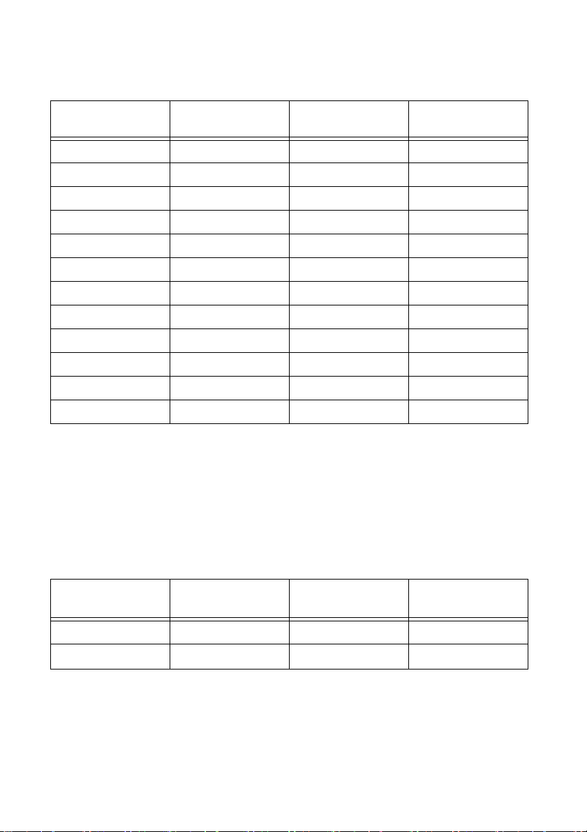
Table 1. Recommended Equipment for NI 5694 Calibration
Equipment
Recommended
Model
Power meter Anritsu ML2438A Characterizing RF source power
Characterizing cable loss
Verifying third-order intercept point
out-of-band
Adjusting IF gain for bypass path
NI PXIe-5694 Calibration Procedure | © National Instruments | 3
Adjusting IF gain
Adjusting IF flatness
Power sensor
(quantity: 2)
Anritsu MA247XD Characterizing RF source power
Characterizing cable loss
Verifying third-order intercept point
out-of-band
Adjusting IF gain for bypass path
Adjusting IF gain
Adjusting IF flatness
Where Used Minimum Requirements
Display resolution: ≤0.01 dB
Settling: ±0.1%
Instrumentation accuracy: <±0.5%
Noise, zero set, and drift: ≤±0.5% full-scale
(lowest range)
Reference power uncertainty: ≤±0.9%
Reference output VSWR: <1.04:1
Power range: -60 dBm to 20 dBm
Frequency range: 10 MHz to 18 GHz
Input VSWR:
10 MHz to 50 MHz .............. <1.90:1
50 MHz to 2 GHz................. <1.12:1
2 GHz to 12.4 GHz .............. <1:22:1
12.4 GHz to 18 GHz ............ <1:25:1
Linearity:
-60 dBm to 20 dBm.............. <1.8%
Calibration factor uncertainty:
10 MHz to 50 MHz .............. <1.9%
50 MHz to 500 MHz ............ <1.5%
500 MHz to 7 GHz............... <1.5%
7 GHz to 12.4 GHz .............. <1.9%
12.4 GHz to 18 GHz ............ <2.3%
Page 4

4 | ni.com | NI PXIe-5694 Calibration Procedure
Table 1. Recommended Equipment for NI 5694 Calibration (Continued)
Equipment
Recommended
Model
Where Used Minimum Requirements
IF digitizer NI PXIe-5622 Adjusting IF gain for bypass path
Adjusting IF gain
Adjusting IF flatness
Signal generators
(quantity: 2,
RF Source 1 and
RF Source 2)
Anritsu MG3692C
Options 2A, 3, 4, 15A,
and 22
Characterizing RF source power
Characterizing cable loss
Verifying third-order intercept point
out-of-band
Adjusting IF gain for bypass path
Adjusting IF gain
Adjusting IF flatness
Spectrum analyzer Rohde & Schwarz
FSU26
Characterizing RF source power
Verifying third-order intercept point
out-of-band
SMA (m)-to-SMA (m)
semi flexible cable
NI 190412B-04 Characterizing RF source power
Characterizing cable loss
198941D-0XL
Frequency range: 8 MHz to 270 MHz
Leveled power: -115 dBm to 18 dBm
Power accuracy: ±1.5 dB
Harmonics (typical):
0.1 MHz to ≤10 MHz ...........<-30 dBc
>10 MHz to ≤100 MHz ........<-40 dBc
>100 MHz to ≤2.2 GHz........<-50 dBc
>2.2 GHz to ≤20 GHz ..........<-30 dBc
Nonharmonic spurious:
0.1 MHz to ≤10 MHz ...........<-30 dBc
>10 MHz to ≤2.2 GHz..........<-60 dBc
>2.2 GHz to ≤20 GHz ..........<-60 dBc
Output VSWR: <2.0:1 (typical)
Frequency range: 10 MHz to 3.6 GHz
Noise floor: <-152 dBm/Hz
Third-order intercept point (entire frequency range):
>10 dBm
—
Page 5

Table 1. Recommended Equipment for NI 5694 Calibration (Continued)
Equipment
SMA (m)-toSMA (m) cable
(quantity: 4)
NI PXIe-5694 Calibration Procedure | © National Instruments | 5
Low-frequency
combiner
SMA (m)-toSMA (f) 10 dB
attenuator (quantity: 2)
Recommended
Model
MegaPhase
G916-SISI-36
Mini Circuits
ZFSC-2-5-S+
Huber+Suhner
6610_SMA-50-1/
199N
Where Used Minimum Requirements
Characterizing RF source power
Characterizing cable loss
Verifying third-order intercept point
out-of-band
Adjusting IF gain for bypass path
Adjusting IF gain
Adjusting IF flatness
Characterizing RF source power
Verifying third-order intercept point
out-of-band
Characterizing RF source power
Verifying third-order intercept point
out-of-band
Length: 36 in.
Frequency range: DC to 18 GHz
Insertion loss: ≤2 dB at 18 GHz
Impedance: 50 Ω
VSWR: ≤1.35:1 at 18 GHz
Frequency range: 10 MHz to 1.5 GHz
Isolation:
10 MHz to 100 MHz ............ ≥15 dB
100 MHz to 750 MHz .......... ≥20 dB
Insertion loss:
10 MHz to 100 MHz ............ ≤3.6 dB
100 MHz to 750 MHz .......... ≤4.0 dB
Connectors: SMA (f)
Frequency range: 10 MHz to 18 GHz
Attenuation: 10 dB (nominal)
Power rating: 2 W average
Impedance: 50 Ω
VSWR: DC to 4 GHz ........... ≤1.15:1
Page 6

6 | ni.com | NI PXIe-5694 Calibration Procedure
Table 1. Recommended Equipment for NI 5694 Calibration (Continued)
Equipment
3.5 mm (m)-to-
3.5 mm (m) adapter
3.5 mm (f)-to-
3.5 mm (f) adapter
BNC (m)-toBNC (m) cable
(quantity: 3)
Recommended
Model
Huber+Suhner
32_PC35-50-0-2/
199_NE
Huber+Suhner
31_PC35-50-0-2/
199_N
— Verifying third-order intercept point
Where Used Minimum Requirements
Verifying third-order intercept point
out-of-band
Adjusting IF gain for bypass path
Adjusting IF gain
Adjusting IF flatness
Frequency range: DC to 33 GHz
Impedance: 50 Ω
Return loss:
DC to 1.5 GHz ...................... ≥35 dB
1.5 GHz to 6.0 GHz .............. ≥30 dB
6.0 GHz to 18.0 GHz ............ ≥20 dB
Characterizing cable loss Frequency range: DC to 18 GHz
Impedance: 50 Ω
Return loss:
DC to 1.5 GHz ...................... ≥35 dB
1.5 GHz to 6.0 GHz .............. ≥30 dB
6.0 GHz to 18.0 GHz ............ ≥20 dB
Length: 36 in.
out-of-band
Impedance: 50 Ω
Adjusting IF gain for bypass path
Adjusting IF gain
Adjusting IF flatness
Page 7

Table 1. Recommended Equipment for NI 5694 Calibration (Continued)
Equipment
Power splitter
(2 resistor type)
NI PXIe-5694 Calibration Procedure | © National Instruments | 7
Recommended
Model
Aeroflex/Weinschel
1593
Where Used Minimum Requirements
Characterizing RF source power
Characterizing cable loss
Adjusting IF gain for bypass path
Adjusting IF gain
Adjusting IF flatness
Frequency range: DC to 26.5 GHz
Amplitude tracking: <0.25 dB
Phase tracking: <4°
Insertion loss: ≤8.5 dB (6 dB, nominal)
Power rating: 1 W
VSWR: DC to 270 MHz....... ≤1.25:1
Equivalent output VSWR:
DC to 270 MHz.................... ≤1.25:1
Connectors: 3.5 mm (f)
Torque wrench — — For SMA connectors: 0.565 N · m (5 lb · in.)
For 3.5mm connectors: 0.90 N · m (8 lb · in.)
Page 8

Test Conditions
The following setup and environmental conditions are required to ensure the NI 5694 meets
published specifications.
• Keep cabling as short as possible. Long cables and wires act as antennas, picking up extra
noise that can affect measurements.
• Verify that all connections, including front panel connections and screws, are secure.
• Maintain an ambient temperature of 23 °C ±5 °C.
• Keep relative humidity between 10% and 90%, noncondensing.
• Allow a warm-up time of at least 30 minutes after the chassis is powered on and NI-RFSA
is loaded and recognizes the NI 5694. The warm-up time ensures that the NI 5694 and test
instrumentation are at stable operating temperature.
• In each verification procedure, insert a delay between configuring all devices and acquiring
the measurement. This delay may need to be adjusted depending on the instruments used
but should always be at least 1,000 ms for the first iteration, 1,000 ms when the power level
changes, and 100 ms for each other iteration.
• Plug the PXI Express chassis and the calibrator into the same power strip to avoid ground
loops.
• Use a torque wrench appropriate for the type of RF connector that you are using.
NI recommends a 0.565 N · m (5 lb · in.) wrench for SMA connectors and a 0.90 N · m
(8 lb · in.) wrench for 3.5 mm connectors.
• Ensure that the PXI Express chassis fan speed is set to HIGH, that the fan filters, if present,
are clean, and that the empty slots contain filler panels. For more information, refer to the
Maintain Forced-Air Cooling Note to Users document, available at
ni.com/manuals.
Initial Setup
Refer to the NI 5694 Getting Started Guide for information about how to install the NI-RFSA
software, the NI 5694 hardware, and how to configure the NI 5694 in Measurement &
Automation Explorer (MAX).
As-Found and As-Left Limits
The as-found limits are the published specifications for the NI 5694. NI uses these limits to
determine whether the NI 5694 meets the device specifications when it is received for
calibration.
The as-left limits are equal to the published NI specifications for the NI 5694, less guard bands
for measurement uncertainty, temperature drift, and drift over time. NI uses these limits to
reduce the probability that the instrument is no longer calibrated at the end of the calibration
cycle.
8 | ni.com | NI PXIe-5694 Calibration Procedure
Page 9

Characterization
Complete each of the following procedures to characterize the test system. The information
obtained in characterization is used when verifying the system behavior.
Caution The connectors on the device under test (DUT) and test equipment are
fragile. Perform the steps in these procedures with great care to prevent damaging any
DUTs or test equipment.
Determining Power Splitter Reference Output
You must designate one of the two power splitter outputs as the reference output. Use only this
output as the reference output for all procedures.
Calibrating Power Sensor Zero Settings
Complete this procedure before beginning any characterization process to ensure that the power
sensor returns appropriate readings.
1. Connect channel A of the power meter to power sensor A.
2. Connect channel B of the power meter to power sensor B.
3. Zero and calibrate the power sensor using the built-in functions in the power meter.
Characterizing RF Source Power
Complete this procedure to characterize the output power of the RF sources through the cables,
attenuators, and combiner. The procedures listed in Verifying Third-Order Intercept Point
Out-of-Band require that the power levels of the sources be in accord with the specification
definition.
Synchronizing the Signal Generators
Complete this procedure to synchronize RF source 1, RF source 2, and the spectrum analyzer to
the same 10 MHz clock reference.
1. Connect the 10 MHz clock reference output on RF source 1 back panel to the 10 MHz clock
reference input on the RF source 2 back panel. Use a BNC (m)-to-BNC (m) cable.
2. Connect the 10 MHz clock reference output on the RF source 2 back panel to the 10 MHz
clock reference input on the spectrum analyzer back panel. Use a BNC (m)-to-BNC (m)
cable.
3. Configure the spectrum analyzer to use the external reference. On the Rohde & Schwarz
FSU26 analyzer, press the Setup button and select External Reference.
NI PXIe-5694 Calibration Procedure | © National Instruments | 9
Page 10

Configuring the Hardware
1
2
5
4
6
7
3
Complete this process to connect the two sources to a power sensor and power meter, preparing
the configuration for verification and characterization. This assembly is used in Verifying
Third-Order Intercept Point Out-of-Band.
1. Connect the spectrum analyzer REF OUT connector to the REF IN connector on the back
of the PXI Express chassis. Use a standard BNC (m)-to-BNC (m) cable.
2. Connect one 10 dB attenuator to a non-common low-frequency combiner connector. Label
both the low-frequency combiner connector and the attenuator P1.
3. Connect the remaining 10 dB attenuator to the remaining non-common low-frequency
combiner connector. Label both the low-frequency combiner connector and the attenuator
P2.
4. Use an SMA (m)-to-SMA (m) cable to connect RF source 1 to the 10 dB attenuator labeled
P1. Label the signal generator Source 1. Label the cable S1P.
5. Use an SMA (m)-to-SMA (m) cable to connect RF source 2 to the 10 dB attenuator labeled
P2. Label the signal generator Source 2. Label the cable S2P.
6. Connect the combiner common connector to power sensor A.
7. Connect channel A of the power meter to power sensor A.
Figure 1. Configuration for Power Level Characterization
1 RF Source 1
2 SMA (m)-to-SMA (m) Cable
3 10 dB Attenuator
10 | ni.com | NI PXIe-5694 Calibration Procedure
4 Low-Frequency Combiner
5 Power Sensor A
6 RF Source 2
7 Power Meter
Page 11

Characterizing the Source Signal Power Levels
Complete this process to characterize the power level of the RF source generators. This
information is required in the verification procedures.
1. Ensure that the RF source 1 generator output is ON and the RF source 2 generator output
is OFF.
2. Set the RF source 1 generator to the first frequency listed in Table 2.
Table 2. Source 1 Signal Characterization
Source 1
Frequency (MHz)
Power Level at
0dBm
Power Level at
-5 dBm
Power Level at
-12 dBm
21.4
163.6
186.1
191.5
193
193.51
193.6
193.765
194.2
195.7
201.1
223.6
3. Adjust the RF source 1 output power until the power level at the low-frequency combiner
common connector, measured by the power meter, is within 0.1 dB of 0 dBm.
4. Record the RF source 1 power level in the empty cell corresponding to the appropriate
frequency and power level.
5. Repeat steps 2 through 4 for each of the remaining frequency and power level combinations
in Table 2. Retain this information for use during the verification procedures.
6. Ensure that the RF source 1 generator output is OFF and the RF source 2 generator output
is ON.
NI PXIe-5694 Calibration Procedure | © National Instruments | 11
Page 12
7. Repeat steps 2 through 4 for each of the frequency and power level combinations in Table 3,
recording the RF source 2 power level in place of RF source 1.
Table 3. Source 2 Signal Characterization
Source 2
Frequency (MHz)
Power Level at
0dBm
Power Level at
-5 dBm
Power Level at
-12 dBm
21.4
133.6
178.6
189.4
192.4
193.27
193.6
193.93
194.8
197.8
208.6
253.6
Characterizing the Source 2 Signal Correction Level
Complete this process to characterize the power level of the RF source 2 generator. This
information is required in the verification procedures.
1. Ensure that the RF source 1 output is OFF and the RF source 2 output is ON.
2. Set the output power level of RF source 2 to -20 dBm.
3. Set RF source 2 to the first frequency listed in Table 4.
Table 4. Signal Correction
Source 2
Frequency (MHz)
Power Meter
Reference (dBm)
Spectrum
Analyzer (dBm)
Correction (dB)
193.6
21.4
4. Record the power level reading on the power meter in the Power Meter Reference cell
corresponding to the appropriate frequency.
5. Repeat steps 3 and 4 for the remaining frequency listed in Table 4.
6. Remove the power sensor from the combiner.
12 | ni.com | NI PXIe-5694 Calibration Procedure
Page 13

7. Connect the low-frequency combiner common connector to the spectrum analyzer RF
1
6
5
2
2
3
4
INPUT connector with the remaining SMA (m)-to-SMA (m) cable. Label the cable DS.
Figure 2. Configuration for Power Level Correction Characterization
1 RF Source 1
2 SMA (m)-to-SMA (m) Cable
8. Configure the spectrum analyzer as follows:
3 10 dB Attenuator
4 Low-Frequency Combiner
5 RF Source 2
6 Spectrum Analyzer
• Center frequency: the first frequency listed in Table 4
• Span: 0 Hz
• Reference level: 10 dBm
• Resolution bandwidth: 100 kHz
• Video bandwidth: 300 kHz
• Number of averages: 100
9. Set RF source 2 to the same frequency configured for the spectrum analyzer in step 8.
10. Record the power level reading on the spectrum analyzer in the Spectrum Analyzer cell in
Table 4 corresponding to the appropriate frequency.
11. Repeat steps 8 through 10 for the remaining frequency listed in Table 4.
12. For each of the two frequencies in Table 4, subtract the value in the Power Meter Reference
cell from the value in the Spectrum Analyzer cell and record it in the Correction cell.
NI PXIe-5694 Calibration Procedure | © National Instruments | 13
Page 14

Characterizing Cable Loss
Complete this procedure to characterize the loss of the system cables.
1. Recalibrate the power sensor zero settings.
2. Ensure that the RF source 1 output is ON and that the RF source 2 output is OFF.
3. Connect power sensor B to the RF source 1 output.
Figure 3. Power Meter to RF Source 1 Direct Connection
1
4
3
1 Power Meter
2 SMA (m)-to-SMA (m) Cable
3 Power Sensor B
4 RF Source 1
4. Configure RF source 1 as follows:
•Power: 0dBm
• Frequency: The first frequency listed in the Frequency column in Table 5
Table 5. Digitizer Cable Loss
Frequency
(MHz)
Reference
Source
Measurement
Digitizer Cable
Loss
Splitter
Tracking Error
(dB)
10
20
30
40
2
RF Source
Cable / Splitter
Loss (dB)
50
60
14 | ni.com | NI PXIe-5694 Calibration Procedure
Page 15

Table 5. Digitizer Cable Loss (Continued)
Frequency
(MHz)
70
80
90
100
107.5
109.1
110.7
112.3
113.9
115.5
117.1
117.5
119.1
120.7
122.3
Reference
Source
Measurement
Digitizer Cable
Loss
Splitter
Tracking Error
(dB)
RF Source
Cable / Splitter
Loss (dB)
123.9
125.5
127.1
128.7
130.3
131.9
133.5
135
135.1
136.6
138.2
NI PXIe-5694 Calibration Procedure | © National Instruments | 15
Page 16

Table 5. Digitizer Cable Loss (Continued)
Frequency
(MHz)
139.8
141.4
143
144.6
146.2
147.8
149.4
151
152.5
152.6
154.1
155.7
157.3
158.9
160.5
Reference
Source
Measurement
Digitizer Cable
Loss
Splitter
Tracking Error
(dB)
RF Source
Cable / Splitter
Loss (dB)
162.1
163.7
165.3
166.9
168.5
170
170.1
171.6
173.2
174.8
176.4
16 | ni.com | NI PXIe-5694 Calibration Procedure
Page 17

Table 5. Digitizer Cable Loss (Continued)
Frequency
(MHz)
178
179.6
181.2
182.8
184.4
186
187.6
189.2
190.8
192.4
193.6
195.2
196.8
198.4
200
Reference
Source
Measurement
Digitizer Cable
Loss
Splitter
Tracking Error
(dB)
RF Source
Cable / Splitter
Loss (dB)
201.6
203.2
204.8
206.4
208
209.6
211.2
212.8
213.5
214.4
215.1
NI PXIe-5694 Calibration Procedure | © National Instruments | 17
Page 18

Table 5. Digitizer Cable Loss (Continued)
Frequency
(MHz)
216.7
218.3
219.9
221.5
223.1
224.7
226.3
227
228.6
230.2
231.8
233.4
235
236.6
238.2
Reference
Source
Measurement
Digitizer Cable
Loss
Splitter
Tracking Error
(dB)
RF Source
Cable / Splitter
Loss (dB)
239.8
240.5
241.4
242.1
243.7
245.3
246.9
248.5
250.1
251.7
253.3
18 | ni.com | NI PXIe-5694 Calibration Procedure
Page 19

Table 5. Digitizer Cable Loss (Continued)
Frequency
(MHz)
Reference
Source
Measurement
Digitizer Cable
Loss
Splitter
Tracking Error
(dB)
RF Source
Cable / Splitter
Loss (dB)
254
255.6
257.2
258.8
260.4
262
263.6
265.2
266.8
268.4
5. Measure the channel B power using the appropriate sensor calibration factor for the
configured frequency. Record this value in the corresponding Reference Source
Measurement cell.
6. Repeat steps 4 and 5 for each frequency listed in Table 5.
7. Disconnect power sensor B from the RF source 1 output.
8. Connect the 3.5mm (m)-to-3.5mm (m) digitizer cable to the RF source 1 output.
NI PXIe-5694 Calibration Procedure | © National Instruments | 19
Page 20

9. Connect power sensor B to the digitizer cable. Use a 3.5 mm (f)-to-3.5 mm (f) adapter.
1
4
2
3
Figure 4. Power Meter-to-Digitizer Cable Connection
1 Power Meter
2 RF Source 1
3 Power Sensor B
4 Digitizer Cable
10. Reset RF source 1 to one of the frequencies listed in the Frequency column in Table 5.
11. Measure the channel B power using the appropriate sensor calibration factor for the
frequency. Use the following equation to calculate and record the Digitizer Cable Loss for
the frequency in Table 5.
Digitizer Cable Loss = Reference Source Measurement - Channel B Power
where Reference Source Measurement is the corresponding measurement
recorded in Table 5 for the frequency.
12. Repeat steps 10 and 11 for each frequency listed in Table 5.
13. Disconnect the digitizer cable and power sensor from the RF source 1 output.
14. Connect the RF source 1 output to the power splitter input. Use a 3.5 mm (m)-to-3.5 mm (m)
RF source cable.
15. Connect the power splitter reference output to power sensor A.
20 | ni.com | NI PXIe-5694 Calibration Procedure
Page 21

16. Connect the remaining power splitter output to power sensor B.
1
2
2
43 5
7
6
Figure 5. Power Meter to Splitter Connection
1 Power Meter
2 SMA (m)-to-SMA (m) Cable
3 Power Sensor B
4 Power Splitter
5 Power Sensor A
6 RF Source Cable
7 RF Source 1
17. Reset RF source 1 to one of the frequencies listed in the Frequency column on Table 5.
18. Measure the channel A power and the channel B power using the appropriate sensor
calibration factor for the frequency. Use the following equation to calculate and record the
Splitter Tracking Error value for the appropriate frequency in Table 5.
Splitter Tracking Error = Channel B Power - Channel A Power
19. Use the following equation to calculate and record the RF Source Cable/Splitter Loss value
for the appropriate frequency in Table 5.
RF Source Cable/Splitter Loss = Reference Source Measurement - Channel B Power
where Reference Source Measurement is the corresponding measurement
recorded in Table 5 for the frequency.
20. Repeat steps 17 through 19 for each frequency in Table 5.
NI PXIe-5694 Calibration Procedure | © National Instruments | 21
Page 22

Verification
The performance verification procedures assume that adequate traceable uncertainties are
available for the calibration references.
Synchronizing the Components
Complete the following procedure to synchronize RF source 1, RF source 2, the spectrum
analyzer, and the PXI Express chassis to the same 10 MHz clock reference.
1. Connect the 10 MHz clock reference output on the RF source 1 back panel to the 10 MHz
clock reference input on the RF source 2 back panel. Use a BNC (m)-to-BNC (m) cable.
2. Connect the 10 MHz clock reference output on the RF source 2 back panel to the 10 MHz
clock reference input on the spectrum analyzer back panel. Use a BNC (m)-to-BNC (m)
cable.
3. Configure the spectrum analyzer to use the external reference. On the Rohde & Schwarz
FSU26 analyzer, press the Setup button and then select External Reference.
4. Connect the 10 MHz clock reference output on the spectrum analyzer back panel to the
10 MHz clock reference input on the PXI Express chassis back panel. Use a
BNC (m)-to-BNC (m) cable.
Configuring the Hardware
Complete the following procedure to configure the hardware for verification.
1. Connect the 10 dB attenuator labeled P1 to the low-frequency combiner connector
labeled P1.
2. Connect the 10 dB attenuator labeled P2 to the low-frequency combiner connector
labeled P2.
3. Connect the signal generator labeled Source 1 to the 10 dB attenuator labeled P1. Use the
SMA (m)-to-SMA (m) cable labeled S1P.
4. Connect the signal generator labeled Source 2 to the 10 dB attenuator labeled P2. Use the
SMA (m)-to-SMA (m) cable labeled S2P.
5. Connect the low-frequency combiner common connector to the NI 5694 IF IN connector.
Use a 3.5 mm (m)-to-3.5 mm adapter.
Note The 3.5 mm (m)-to-3.5 mm adapter is uncharacterized and represents an
uncertainty. This uncertainty is absorbed into the product specifications.
22 | ni.com | NI PXIe-5694 Calibration Procedure
Page 23

6. Connect the NI 5694 IF OUT connector to the spectrum analyzer RF INPUT connector.
Use the SMA (m)-to-SMA (m) cable labeled DS.
Figure 6. Configuration for System Verification
1
2
5
7
1 RF Source 1
2 SMA (m)-to-SMA (m) Cable
3 10 dB Attenuator
IF Conditioning Module
ACCESS ACTIVE
4
3
IF
OUT
187.5 MHz/
193.6 MHz/
21.4 MHz
+22 dBm MAX
0 VDC MAX
IF
IN
187.5 MHz/
193.6 MHz
+18 dBm MAX
12 VDC MAX
REF/LO
IN
10 MHz/
215 MHz
+10 dBm NOM, +18 dBm MAX
12 VDC MAX
REF
OUT
10 MHz
+10 dBm NOM
12 VDC MAX
LO
OUT
215 MHz
+10 dBm NOM
12 VDC MAX
2
4 Low-Frequency Combiner
5 NI 5694
6 SMA (m)-to-SMA (m) Cable
ESD
SENSITIVE
7 RF Source 2
8 Spectrum Analyzer
6
8
NI PXIe-5694 Calibration Procedure | © National Instruments | 23
Page 24

Verifying Third-Order Intercept Point Out-of-Band
Complete the following procedures to determine the as-found status of the NI 5694. Third-order
intercept point out-of-band (TOI-OB) places one signal within the passband and a second signal
outside the passband.
Note Refer to the values recorded during system characterization to complete these
procedures.
Determining the Path Gain
Complete the following procedure to determine system path gain.
1. Ensure that the RF source 1 output is OFF and the RF source 2 output is ON.
2. Configure the RF source 2 generator as follows:
• Power level: -20 dBm
• Frequency: 193.6 MHz
3. Configure the spectrum analyzer as follows:
• Center frequency: 193.6 MHz
• Span: 0 Hz
• Reference level: 0 dBm
• Resolution bandwidth: 10 kHz
• Video bandwidth: 30 kHz
• Number of averages: 100
4. Configure the NI 5694 as follows:
• Reference level: -30 dBm
• IF output power level: +10 dBm
• IF conditioning downconversion enabled: Disabled
• Device instantaneous bandwidth: The first value shown in the Device Instantaneous
Bandwidth column in Table 6
• Step gain: The value in the Step Gain column in Table 6 corresponding to the
configured device instantaneous bandwidth
Table 6. Path Gain, Downconversion Disabled
Device
Instantaneous
Bandwidth (Path)
20 MHz
5 MHz
24 | ni.com | NI PXIe-5694 Calibration Procedure
Step Gain
Disabled
Enabled
Disabled
Enabled
IF OUT Power
(dBm)
Path Gain
Page 25

Table 6. Path Gain, Downconversion Disabled (Continued)
Device
Instantaneous
Bandwidth (Path)
Step Gain
IF OUT Power
(dBm)
Path Gain
1.4 MHz
Disabled
Enabled
Disabled
400 kHz
Enabled
Disabled
110 kHz
Enabled
5. Execute a sweep using the spectrum analyzer and record the peak marker reading in the
appropriate IF OUT Power cell in Table 6.
6. Use the following formula to compute the path gain and record it in the corresponding Path
Gain cell.
Path Gain = P
SA
- P
CORR
- P
REF
where:
P
= IF OUT Power recorded in Table 6
SA
P
= Characterized correction recorded in Table 4 for the configured
CORR
frequency
P
= Characterized reference power recorded in Table 4 for the configured
REF
frequency
7. Repeat steps 4 through 6 for each of the remaining values in the Device Instantaneous
Bandwidth column in Table 6.
8. Reconfigure the spectrum analyzer as follows:
• Center frequency: 21.4 MHz
• Span: 0 Hz
• Reference level: 10 dBm
• Resolution bandwidth: 10 kHz
• Video bandwidth: 30 kHz
• Number of averages: 100
NI PXIe-5694 Calibration Procedure | © National Instruments | 25
Page 26

9. Reconfigure the NI 5694 as follows:
• Reference Clock source: PXI_Clk
• Reference level: -30 dBm
• IF output power level: +10 dBm
• Downconversion enabled: TRUE
• Device instantaneous bandwidth: The first value shown in the Device Instantaneous
Bandwidth column in Table 7
• Step gain: The value in the Step Gain column in Table 7 corresponding to the
configured device instantaneous bandwidth
Table 7. Path Gain, Downconversion Enabled
Device
Instantaneous
Bandwidth (Path)
Step Gain
IF OUT Power
(dBm)
Path Gain
20 MHz
Disabled
Enabled
Disabled
5 MHz
Enabled
Disabled
1.4 MHz
Enabled
Disabled
400 kHz
Enabled
Disabled
110 kHz
Enabled
Disabled
30 kHz
Enabled
10. Record the power reported by the spectrum analyzer in the appropriate IF OUT Power cell
in Table 7.
11. Use the formula from step 6 to compute the path gain and record it in the corresponding
Path Gain cell in Table 7.
12. Repeat steps 9 through 11 for each of the remaining values in the Device Instantaneous
Bandwidth column in Table 7.
26 | ni.com | NI PXIe-5694 Calibration Procedure
Page 27

Verifying Third-Order Intercept Point Out-of-Band At Multiple Input Power Levels
Complete the following procedure to verify TOI-OB at multiple input power levels and
downconversion settings.
1. Ensure that the RF source 1 output and the RF source 2 output are both ON.
2. Configure the spectrum analyzer as follows:
• Frequency: 193.6 MHz
• Span: 0 Hz
• Reference level: -40 dBm
• RBW: 10 Hz
• VBW: 30 Hz
• Number of averages: 30
3. Configure the NI 5694 as follows:
• Reference level: -30 dBm
• IF output power level: +10 dBm
• Step gain: Disabled
• IF conditioning downconversion enabled: Disabled
• Device instantaneous bandwidth: The first value listed in the Device Instantaneous
Bandwidth column in Table 8
Table 8. TOI-OB Calculation,
DUT Input Power 0 dBm, Downconversion Disabled
Device
Instantaneous
Bandwidth
(Path)
20 MHz
5 MHz
1.4 MHz
400 kHz
110 kHz
RF Source 1
Frequency
(MHz)
223.6 253.6
163.6 133.6
201.1 208.6
186.1 178.6
195.7 197.8
191.5 189.4
194.2 194.8
193 192.4
193.765 193.93
193.51 193.27
RF Source 2
Frequency
NI PXIe-5694 Calibration Procedure | © National Instruments | 27
(MHz)
IF OUT Power
(dBm)
TOI-OB (dBm)
Page 28

4. Set RF source 1 to the first frequency listed in the RF Source 1 Frequency column of
TOI
OB
P
IN
P
INPOIMDGK
–()–
2
--------------------------------------------------+=
Table 8 corresponding to the configured device instantaneous bandwidth.
5. Set the RF source 1 output power to the appropriate characterized power recorded in
Table 2 for the configured RF source 1 frequency and a device under test (DUT) input
power of 0 dBm.
6. Set RF source 2 to the frequency listed in the RF Source 2 Frequency column of Table 8
corresponding to the configured RF source 1 frequency.
7. Set the RF source 2 output power to the characterized power recorded in Table 3
corresponding to the configured RF source 2 frequency and a DUT input power of 0 dBm.
8. Use the following equation to compute the IF OUT power and record the result in the
corresponding cell in the IF OUT Power column in Table 8.
IF OUT Power = P
- P
SA
CORR
where:
P
= Power reported by the spectrum analyzer
SA
P
= Characterized correction (dB) recorded in Table 4 for the frequency
CORR
193.6 MHz
9. Repeat steps 3 through 8 for each of the remaining combinations of device instantaneous
bandwidth, RF source 1 frequency, and RF source 2 frequency listed in Table 8.
10. Calculate the TOI-OB for the configured RF source 1 and RF source 2 frequencies using
the following formula. Record the result in the corresponding cell in the TOI-OB cell in
Table 8.
where:
= TOI out-of-band in dBm
TOI
OB
P
= Configured DUT input power, in this case 0 dBm
IN
P
= The greater of the two values recorded in the IF OUT Power column in
OIMD
Table 8 for the configured device instantaneous bandwidth
= The value recorded in the Path Gain column in Table 6 for the configured
G
K
device instantaneous bandwidth with step gain disabled
11. Repeat step 10 for each combination of frequencies listed in Table 8.
12. Reconfigure the NI 5694, enabling step gain.
28 | ni.com | NI PXIe-5694 Calibration Procedure
Page 29

13. Repeat steps 4 through 11 with the new settings and the following changes:
• When configuring RF source 1 and 2 output power, use a device under test (DUT)
input power of -5 dBm instead of -0 dBm.
• Record your results using Table 9.
Table 9. TOI-OB Calculation,
DUT Input Power -5 dBm (per Tone), Downconversion Disabled
Device
Instantaneous
Bandwidth (Path)
RF Source 1
Frequency
(MHz)
RF Source 2
Frequency
(MHz)
IF OUT
Power
(dBm)
TOI- OB
(dBm)
223.6 253.6
20 MHz
163.6 133.6
201.1 208.6
5 MHz
186.1 178.6
195.7 197.8
1.4 MHz
191.5 189.4
194.2 194.8
400 kHz
186.1 178.6
193.765 193.93
110 kHz
193.435 193.51
14. Reconfigure the spectrum analyzer for a frequency of 21.4 MHz.
15. Reconfigure the NI 5694, enabling IF conditioning downconversion and disabling step
gain.
NI PXIe-5694 Calibration Procedure | © National Instruments | 29
Page 30

16. Repeat steps 4 through 18 with the new settings and the following changes:
• When configuring RF source 1 and 2 output power, use a device under test (DUT)
input power of -5 dBm instead of -0 dBm.
• Record your results using Table 10.
Table 10. TOI-OB Calculation,
DUT Input Power -5 dBm (per Tone), Downconversion Enabled
Device
Instantaneous
Bandwidth (Path)
RF Source 1
Frequency
(MHz)
RF Source 2
Frequency
(MHz)
IF OUT
Power
(dBm)
Out-of-Band
201.1 208.6
5 MHz
186.1 178.6
195.7 197.8
1.4 MHz
191.5 189.4
194.2 194.8
400 kHz
193 192.4
193.765 193.93
110 kHz
193.435 193.27
193.645 193.69
30 kHz
193.555 193.51
17. Repeat steps 4 through 18 with the following changes:
• When configuring RF source 1 and 2 output power, use a device under test (DUT)
input power of -12 dBm instead of -0 dBm.
• Reconfigure the NI 5694 to enable step gain.
• Record your results using Table 11.
TOI
(dBm)
Table 11. TOI-OB Calculation,
DUT Input Power -12 dBm (per Tone), Downconversion Enabled
Device
Instantaneous
Bandwidth (Path)
RF Source 1
Frequency
(MHz)
201.1 208.6
5 MHz
186.1 178.6
195.7 197.8
1.4 MHz
191.5 189.4
30 | ni.com | NI PXIe-5694 Calibration Procedure
RF Source 2
Frequency
(MHz)
IF OUT
Power
(dBm)
TOI- OB
(dBm)
Page 31

Table 11. TOI-OB Calculation,
DUT Input Power -12 dBm (per Tone), Downconversion Enabled (Continued)
Device
Instantaneous
Bandwidth (Path)
RF Source 1
Frequency
(MHz)
RF Source 2
Frequency
(MHz)
IF OUT
Power
(dBm)
TOI- OB
(dBm)
194.2 194.8
400 kHz
193 192.4
193.765 193.93
110 kHz
193.435 193.51
193.645 193.69
30 kHz
193.555 193.51
18. Compare each of the values you recorded in the PATH TOI-OB column in each of the
previous tables to the values listed in Table 12. If the value is equal to or greater than the
value listed the table, the device passes verification. If the value is less than the value listed
in the table, the device fails verification.
Table 12. TOI Verification Test Limits
Test Condition As-Found Limit As-Left Limit*
Downconversion: Disabled
40 dBm 41 dBm
Gain: Off
Downconversion: Disabled
32 dBm 33 dBm
Gain: On
Downconversion: Enabled
29 dBm 30 dBm
Gain: Off
Downconversion: Enabled
25 dBm 26 dBm
Gain: On
* The as-left limits cannot be linearly combined with the measurement uncertainty values to equal the
warranted device specifications. Refer to the As-Found and As-Left Limits section of this document for
more information about as-left limits
NI PXIe-5694 Calibration Procedure | © National Instruments | 31
Page 32

Adjustment
ACCESS ACTIVE
IF Conditioning Module
NI PXIe-5694
ESD
SENSITIVE
REF/LO
IN
10 MHz/
215 MHz
+10 dBm NOM, +18 dBm MAX
12 VDC MAX
IF
OUT
187.5 MHz/
193.6 MHz/
21.4 MHz
+22 dBm MAX
0 VDC MAX
IF
IN
187.5 MHz/
193.6 MHz
+18 dBm MAX
12 VDC MAX
REF
OUT
10 MHz
+10 dBm NOM
12 VDC MAX
LO
OUT
215 MHz
+10 dBm NOM
12 VDC MAX
1
2
7
43 65
8
ACCESS ACTIVE
CLK IN
CLK OUT
PFI 1
ESD
SENSITIVE
TTL
6.3 Vp-p
MAX
2 Vp-p
NOM
+
20 dBm MAX
50 Ω
50 Ω
50 Ω
NI PXIe-5622
16-Bit IF Digitizer
IF IN
Complete the following procedures to adjust the NI 5694. Following the adjustment procedures
automatically updates the calibration date and temperature in the EEPROM of the NI 5694.
Note National Instruments recommends a complete adjustment of your device to
renew the calibration interval.
Configuring the Hardware
Complete the following procedure to configure the hardware for adjustment.
1. Connect RF source 1 to the power splitter input. Use an SMA (m)-to-SMA (m) cable.
2. Connect Power Sensor A to power meter channel A and to one output of the power splitter.
3. Connect the remaining power splitter output to the NI 5694 IF IN connector. Use an
SMA(m)-to-SMA(m) adapter.
4. Connect the NI 5694 IF OUT connector to the NI 5622 digitizer IF IN connector. Use an
SMA (m)-to-SMA (m) cable.
Figure 7. Hardware Configuration for Adjustment
1 RF Source 1
2 Power Sensor A
3 Power Splitter
4 NI 5694
5 SMA (m)-to-SMA (m) Cable
6 NI 5622 Digitizer
32 | ni.com | NI PXIe-5694 Calibration Procedure
7 SMA (m)-to-SMA (m) Cable
8 Power Meter
Page 33

Adjusting IF Gain for Bypass Path
Complete the following procedure to measure and adjust the IF gain for bypass path
performance of the NI 5694 IF conditioning module.
1. Zero and calibrate the power sensors using the built-in functions in the power meter.
2. Ensure that the hardware is properly configured as described in Configuring the Hardware.
3. Run the self-calibration procedure for the NI 5622 digitizer.
4. Initialize an external calibration session for the NI 5694.
5. Initialize an IF attenuation calibration step.
6. Configure the NI 5694 as follows:
• Signal conditioning: Bypassed
• IF conditioning downconversion: Disabled
• Step gain: Disabled
7. Configure RF source 1 as follows:
• Single frequency mode
• Frequency: 107.5 MHz
• Power level: 0 dBm
8. Configure the power meter as follows:
• Channel 1: Power sensor A
• Trigger with settling delay
• Sensor setting: 0.1%
9. Configure the NI 5622 digitizer as follows:
• Sampling rate: 585.9375 kS/s
• Number of samples to acquire: 40,960
• Reference source: PXI_Clk
• Reference Clock rate: 100 MHz
• DDC enabled: TRUE
• Data processing mode: Complex
• Frequency translation enables: TRUE
• DDC center frequency: 107.5 MHz
• Dither enabled: FALSE
• Bandpass filter enabled: FALSE
10. Read the power meter channel A power.
11. Calculate the NI 5694 IF input power using the following equation:
IF Input Power = Channel A Power + Splitter Tracking at RF Source Frequency
NI PXIe-5694 Calibration Procedure | © National Instruments | 33
Page 34

12. Acquire a complex record with the NI 5622 digitizer and compute the digitizer power in
Digitizer Power 10 log10×
1
N
--- -
I
j
2
Q
j
2
+()
j 0=
N 1–
10+=
dBm using the following equation:
where:
N = Number of samples to acquire
I
= Real part of the jth complex sample
j
= Imaginary part of the jth complex sample
Q
j
13. Query the NI 5622 digitizer frequency response and retrieve the value at the DDC center
frequency by linear interpretation.
14. Calculate the NI 5694 gain using the following equation:
Gain = Digitizer Power + Digitizer Cable Loss - Digitizer Frequency Response - Input Power
Note Refer to Table 5 for the characterized digitizer cable loss.
15. Record the calculated gain and the RF input frequency value to the NI 5694 EEPROM.
16. Increase the RF source 1 frequency and the digitizer DDC center frequency by 1.6 MHz.
17. Repeat steps 10 through 16 for all frequencies up to and including 267.5 MHz.
18. Close the IF attenuation calibration step.
19. Close the external calibration session.
Adjusting IF Gain
Complete the following procedure to measure and adjust the IF gain performance of the NI 5694
IF conditioning module.
1. Zero and calibrate the power sensors using the built-in functions in the power meter.
2. Ensure that the hardware is properly configured as described in Configuring the Hardware.
3. Run the self-calibration procedure of the NI 5622 digitizer.
4. Initialize an external calibration session for the NI 5694.
5. Initialize an IF attenuation calibration step.
6. Configure the NI 5694 as follows:
• Signal conditioning: Enabled
• Reference source: PXI_Clk
• IF conditioning downconversion: Disabled
• Step gain: Disabled
34 | ni.com | NI PXIe-5694 Calibration Procedure
Page 35

7. Configure RF source 1 as follows:
Digitizer Power 10 log10×
1
N
--- -
I
j
2
Q
j
2
+()
j 0=
N 1–
10+=
• Single frequency mode
• Frequency: 193.6 MHz
• Power level: -6 dBm
8. Configure the power meter as follows:
• Channel 1: Power sensor A
• Trigger with settling delay
• Sensor setting: 0.1%
9. Configure the digitizer as follows:
• Sampling rate: 585.9375 kS/s
• Number of samples to acquire: 40,960
• Reference source: PXI_Clk
• Reference Clock rate: 100 MHz
• DDC enabled: TRUE
• Data processing mode: Complex
• Frequency translation enabled: TRUE
• DDC center frequency: 193.6 MHz
• Dither enabled: FALSE
• Bandpass filter enabled: TRUE
10. Set the NI 5694 IF filter to 20 MHz.
11. Read the power meter channel A power.
12. Calculate the NI 5694 IF input power using the following equation:
13. Set IF Attenuation Table Index to 0.
14. Acquire a record of complex samples with the NI 5622 digitizer and compute the digitizer
power in dBm using the following equation:
where:
15. Query the NI 5622 digitizer frequency response and retrieve the value at 193.6 MHz by
linear interpolation.
IF Input Power = Channel A Power + Splitter Tracking at 193.6 MHz
N = Number of samples to acquire
I
= Real part of the jth complex sample
j
= Imaginary part of the jth complex sample
Q
j
NI PXIe-5694 Calibration Procedure | © National Instruments | 35
Page 36

16. Calculate the NI 5694 gain using the following equation:
Gain = Digitizer Power + Digitizer Cable Loss - Digitizer Frequency Response - Input Power
Note Refer to Table 5 for the characterized digitizer cable loss.
17. Record the calculated gain to the NI 5694 EEPROM along with the RF source 1 frequency.
18. Repeat steps 13 through 17 for IF Attenuation Table Index values from 1 to 25, with a step
size of 1.
19. Repeat steps 10 through 18 for each of the following IF filter frequency settings:
•5 MHz
• 1.4 MHz
• 400 kHz
• 110 kHz
20. Reconfigure the NI 5694 to enable step gain.
21. Reconfigure RF source 1, adjusting the power level to -15 dBm.
22. Repeat steps 10 through 19 with the new settings.
23. Reconfigure the NI 5622 digitizer as follows:
• DDC center frequency: 21.4 MHz
• Bandpass filter enabled: FALSE
24. Reconfigure the NI 5694 as follows:
• Step gain: Disabled
• IF conditioning downconversion: Enabled
25. Repeat steps 10 through 19 with the new settings and the following changes:
• In step 15, query the digitizer response at 21.4 MHz instead of 193.6 MHz
• In step 19, add 30 kHz to the list of frequencies to be iterated over
26. Reconfigure RF source 1, adjusting the power level to -25 dBm.
27. Reconfigure the NI 5694, enabling step gain.
28. Repeat steps 10 through 19 with the new settings and the following changes:
• In step 15, query the digitizer response at 21.4 MHz instead of 193.6 MHz
• In step 19, add 30 kHz to the list of frequencies to measure
29. Close the IF attenuation calibration step.
30. Close the external calibration session.
36 | ni.com | NI PXIe-5694 Calibration Procedure
Page 37

Adjusting IF Flatness
Complete the following procedure to measure and adjust the IF flatness performance of the
NI 5694 IF conditioning module.
1. Zero and calibrate the power sensors using the built-in functions in the power meter.
2. Ensure that the hardware is properly configured as described in Configuring the Hardware.
3. Run the self-calibration procedure of the NI 5622 digitizer.
4. Initialize an external calibration session for the NI 5694.
5. Initialize an IF response calibration step.
6. Configure the NI 5694 as follows:
• Signal conditioning: Enabled
• Reference source: PXI_Clk
• IF conditioning downconversion: Disabled
• Step gain: Disabled
7. Configure the RF source 1 generator as follows:
• Single frequency mode
• Frequency: 193.6 MHz
• Power level: -6 dBm
8. Configure the power meter as follows:
• Channel 1: Power sensor A
• Trigger with settling delay
• Sensor setting %: 0.1
9. Configure the digitizer as follows:
• Sampling rate: 585.9375 kS/s
• Number of samples to acquire: 40,960
• Reference source: PXI_Clk
• Reference Clock rate: 100 MHz
• DDC enabled: TRUE
• Data processing mode: Complex
• Frequency translation enabled: TRUE
• Dither enabled: TRUE
• Bandpass filter enabled: TRUE
NI PXIe-5694 Calibration Procedure | © National Instruments | 37
Page 38

10. Set the NI 5694 IF filter to the first value listed in Table 13.
Current Frequency Offset Lower RF Frequency Offset j
Measurement Span
Number of Frequency Points 1–
----------------------------------------------------------------------------- -
+=
Table 13. IF Flatness Measurement Settings
Measurement
IF Filter
20 MHz 32 MHz -16 MHz
5 MHz 10 MHz -5 MHz
1.4 MHz 2 MHz -1 MHz
400 kHz 600 kHz -300 kHz
110 kHz 220 kHz -110 kHz
30 kHz 40 kHz -20 kHz
Span
Lower RF
Frequency Offset
Number of Frequency Points
IF attenuation index = 5 51
All other indexes 15
IF attenuation index = 5 41
All other indexes 11
IF attenuation index = 5 51
All other indexes 21
IF attenuation index = 5 31
All other indexes 11
IF attenuation index = 5 31
All other indexes 21
IF attenuation index = 5 61
All other indexes 21
11. Set the NI 5694 IF attenuation table index to 0.
12. Calculate the list of RF frequency offsets using the following equation:
where:
Lower RF Frequency Offset = The value displayed in Table 13 corresponding to
the configured IF filter
j = A range from 0 to Number of Frequency Points - 1
Measurement Span = The value displayed in Table 13 corresponding to the
configured IF filter
Number of Frequency Points = The value displayed in Table 13 corresponding to
the configured IF filter
13. Set the frequency of RF source 1 to 193.6 MHz plus the current frequency offset calculated
in step 12.
14. Read the power meter channel A power.
15. Calculate the NI 5694 IF input power using the following equation:
Input Power = Channel A Power + Splitter Tracking at Current RF Source Frequency
38 | ni.com | NI PXIe-5694 Calibration Procedure
Page 39

16. Set the NI 5622 digitizer DDC center frequency to the RF source 1 frequency.
Digitizer Power 10 log10×
1
N
--- - I
j
2
Q
j
2
+()
j 0=
N 1–
10+=
17. Acquire a record of complex samples with the NI 5622 digitizer and compute the digitizer
power using the following equation:
where:
N = Number of samples to acquire
I
= Real part of the jth complex sample
j
Q
= Imaginary part of the jth complex sample
j
18. Query the NI 5622 frequency response and retrieve the value at the current DDC center
frequency by using linear interpolation.
19. Calculate the NI 5694 gain using the following equation:
Gain = Digitizer Power + Digitizer Cable Loss - Digitizer Frequency Response - Input Power
Note Refer to Table 5 for the characterized digitizer cable loss.
20. Record the calculated gain and the current frequency of RF source 1 to the NI 5694
EEPROM.
21. Repeat steps 13 through 20 for all the values in the frequency list computed in step 12.
22. Repeat steps 11 through 21 for IF attenuation table index values from 1 to 25, with a step
size of 1.
23. Repeat steps 10 through 22 for each of the following IF filter values:
•5 MHz
• 1.4 MHz
• 400 kHz
• 110 kHz
24. Reconfigure the NI 5694, enabling step gain.
25. Reconfigure RF source 1 for a power level of -15 dBm.
26. Repeat steps 10 through 23 with the new settings.
27. Reconfigure the NI 5622 digitizer, disabling the bandpass filter.
28. Reconfigure the NI 5694 as follows:
• Step gain: Disabled
• IF conditioning downconversion: Enabled
29. Repeat steps 10 through 23 with the new settings and the following changes:
• In step 16, set the DDC center frequency to 215 MHz - RF Source 1 Frequency
• In step 23, add 30 kHz to the list of frequencies to measure
30. Reconfigure RF source 1 for a power level of -25 dBm.
31. Reconfigure the NI 5694, enabling step gain.
NI PXIe-5694 Calibration Procedure | © National Instruments | 39
Page 40

32. Repeat steps 10 through 23 with the new settings and the following changes:
• In step 16, set the DDC center frequency to 215 MHz - RF Source 1 Frequency
• In step 23, add 30 kHz to the list of frequencies to measure
33. Close the IF response calibration step.
34. Close the external calibration session.
Reverification
Repeat the Verification section to determine the as-left status of the device.
Note If any test fails reverification after performing an adjustment, verify that you
have met the Test Conditions before returning your device to NI. Refer to Worldwide
Support and Services for information about support resources or service requests.
Worldwide Support and Services
The National Instruments website is your complete resource for technical support. At ni.com/
support
self-help resources to email and phone assistance from NI Application Engineers.
Vis it
other services.
Vis it
facilitates technical support and ensures that you receive important information updates from NI.
you have access to everything from troubleshooting and application development
ni.com/services for NI Factory Installation Services, repairs, extended warranty, and
ni.com/register to register your National Instruments product. Product registration
A Declaration of Conformity (DoC) is our claim of compliance with the Council of the European
Communities using the manufacturer’s declaration of conformity. This system affords the user
protection for electromagnetic compatibility (EMC) and product safety. You can obtain the DoC
for your product by visiting
you can obtain the calibration certificate for your product at
ni.com/certification. If your product supports calibration,
ni.com/calibration.
National Instruments corporate headquarters is located at 11500 North Mopac Expressway,
Austin, Texas, 78759-3504. National Instruments also has offices located around the world. For
telephone support in the United States, create your service request at
ni.com/support or dial
1 866 ASK MYNI (275 6964). For telephone support outside the United States, visit the
Worldwide Offices section of ni.com/niglobal to access the branch office websites, which
provide up-to-date contact information, support phone numbers, email addresses, and current
events.
Refer to the NI Trademarks and Logo Guidelines at ni.com/trademarks for more information on National Instruments trademarks. Other
product and company names mentioned herein are trademarks or trade names of their respective companies. For patents covering National
Instruments products/technology, refer to the appropriate location: Help»Patents in your software, the patents.txt file on your media, or the
National Instruments Patents Notice at ni.com/patents. You can find information about end-user license agreements (EULAs) and third-party
legal notices in the readme file for your NI product. Refer to the Export Compliance Information at ni.com/legal/export-compliance
for the National Instruments global trade compliance policy and how to obtain re levant HTS codes, ECCNs, and other import/export data. NI MAKES
NO EXPRESS OR IMPLIED WARRANTIES AS TO THE ACCURACY OF THE INFORMATION CONTAINED HEREIN AND SHALL NOT BE LIABLE FOR
ANY ERRORS. U.S. Government Customers: The data contained in this manual was developed at private expense and is subject to the applicable
limited rights and restricted data rights as set forth in FAR 52.227-14, DFAR 252.227-7014, and DFAR 252.227-7015.
© 2013–2014 National Instruments. All rights reserved.
374004C-01 Oct14
 Loading...