

Page 1

CALIBRATION PROCEDURE
PXIe-5185/5186
This document contains information for calibrating National Instruments PXIe-5185/5186
digitizers. The PXIe-5185/5186 digitizers were developed jointly between Tektronix and
National Instruments. The devices use Tektronix, Enabling Technology
™
to deliver wide analog
bandwidth and high-speed sampling on the National Instruments Synchronization and Memory
Core (SMC) technology with TClk synchronization.
For more information on calibration, visit
ni.com/calibration.
Contents
50 Ω and 1 MΩ Devices ...........................................................................................................2
Software Requirements............................................................................................................. 2
Related Documentation ............................................................................................................2
Password ..................................................................................................................................3
Calibration Interval...................................................................................................................3
Test Equipment.........................................................................................................................3
Test Conditions.........................................................................................................................5
Calibration Procedures .............................................................................................................6
Initial Setup....................................................................................................................... 6
Self-Calibration ................................................................................................................6
MAX......................................................................................................................... 7
NI-SCOPE Soft Front Panel ..................................................................................... 7
NI-SCOPE ................................................................................................................ 7
External Calibration.......................................................................................................... 7
Test System Characterization ........................................................................................... 7
Zeroing the Power Sensor......................................................................................... 8
Characterizing Power Splitter Amplitude Imbalance............................................... 8
Verification....................................................................................................................... 14
Verifying DC and Programmable Vertical Offset Accuracy.................................... 14
Verifying 50 Ω AC Amplitude Accuracy and Bandwidth .......................................17
Verifying 1 MΩ AC Amplitude Accuracy and Bandwidth...................................... 20
Verifying Timebase Accuracy.................................................................................. 23
Adjustment........................................................................................................................ 23
Worldwide Support and Services ............................................................................................. 29
Page 2

2 | ni.com | PXIe-5185/5186 Calibration Procedure
50 Ω and 1 MΩ Devices
Early versions of the PXIe-5185/5186 support only 50 Ω input impedance. Check the part
number of your device to see what input impedance is supported by your device:
• PXIe-5185 module part numbers 199363x-0zL and PXIe-5186 module part numbers
193537x-0zL (where x is any letter and z is any number) only support 50 Ω input
impedance. These devices require NI-SCOPE 3.8.7 or later.
• PXIe-5185 module part numbers 152962x-0zL and PXIe-5186 module part numbers
152961x-0zL (where x is any letter and z is any number) support both 50 Ωand 1 MΩ input
impedance. These devices require NI-SCOPE 3.9.6 or later.
50 Ωdevices need to be tested for only 50 Ωinput impedance because they have no 1 MΩ input.
Software Requirements
Calibrating the PXIe-5185/5186 requires installing the NI-SCOPE instrument driver on the
calibration system. Refer to the 50 Ω and 1 MΩ Devices section to see which driver version your
device requires. You can download the NI-SCOPE instrument driver from the NI website at
ni.com/downloads/drivers. NI-SCOPE supports programming a self-calibration and an
external calibration in multiple application development environments (ADEs). When you
install NI-SCOPE, you need to install support for only the ADE that you intend to use.
LabVIEW support is in the
niScope.llb file, and all calibration functions appear in the
NI-SCOPE Calibration palette. For LabWindows
™
/CVI™ users, the NI-SCOPE function panel,
niScope.fp, provides access to the available functions.
For the locations of files you may need to calibrate your device, refer to the NI-SCOPE Readme,
which is available on the NI-SCOPE media.
Related Documentation
For information about NI-SCOPE and the PXIe-5185/5186, consult the following documents:
• NI High-Speed Digitizers Getting Started Guide—provides instructions for installing and
configuring the PXIe-5185/5186.
• NI High-Speed Digitizers Help—includes detailed information about the PXIe-5185/5186
and NI-SCOPE VIs and functions and information about creating applications using
NI-SCOPE.
• PXIe-5185 Specifications—provides the published specification values for the PXIe-5185.
• PXIe-5186 Specifications—provides the published specification values for the PXIe-5186.
These documents are installed with NI-SCOPE. You can also find the latest versions of the
documentation at
ni.com/manuals.
Page 3

PXIe-5185/5186 Calibration Procedure | © National Instruments | 3
Password
The default calibration password is NI.
Calibration Interval
NI recommends a calibration interval of one year to ensure the warranted specifications for the
PXIe-5185/5186 are met.
Test Equipment
National Instruments recommends that you use the equipment in Table 1 for calibrating the
PXIe-5185/5186. If you do not have the recommended instruments, use these specifications to
select a substitute calibration standard.
Table 1. PXIe-5185/5186 Test Equipment
Equipment
Recommended
Model
Requirements
Oscilloscope
calibrator
Fluke 9500B/3200 DC Output Range: 2 V to -2 V into 50 Ω,
6.5V to - 6.5 V into 1 MΩ
DC Voltage Accuracy: DC ±0.3% of output
into 50 Ω and 1 MΩ
Leveled Sine Wave Amplitude Range:
0.9 V
pk-pk
into 50 Ω
Leveled Sine Wave Frequency Accuracy:
±4 ppm
Square Wave: 8.0 V
pk-pk
at 100 kHz
into 1 MΩ
3.2 GHz output
module
Fluke 9530 Active
Head
Power sensor Rohde & Schwarz
NRP-Z91
Range: -26 dBm to 10 dBm
Frequency range: 50 kHz to 5.0 GHz
Absolute power accuracy:
• <0.048 dB at 50 kHz
• <0.063 dB at 5.0 GHz
Relative power accuracy:
• <0.022 dB at 50 kHz
• <0.031 dB for frequencies > 50 kHz and
< 5.0 GHz
VSWR: <1.11
Page 4

4 | ni.com | PXIe-5185/5186 Calibration Procedure
Signal generator Rohde & Schwarz
SMA100A
Frequency range: 50 kHz to 5.0 GHz
Amplitude range: -20 dBm to 16 dBm
Harmonics: <-30 dBc
Power splitter Aeroflex/Weinschel Frequency range: 50 kHz to 5.0 GHz
VSWR: <1.1
Amplitude tracking: <0.5 dB
50 Ω BNC
terminator (f)
Fairview Microwave
ST3B-F
Frequency range: DC to 0.5 GHz
VSWR: <1.2
Impedance: 50 Ω
50 Ω SMA
terminator (f)
Fairview Microwave
ST1852F
Frequency range: DC to 5.0 GHz
VSWR: <1.1
Impedance: 50 Ω
SMA (m)-toSMA (m) cable
— Frequency range: DC to 5.0 GHz
VSWR: <1.1
Length: ≤1 meter
SMA (m)-toBNC (f)
Fairview Microwave
SM4723
Frequency range: DC to 100 kHz
Impedance: 50 Ω
SMA (f)-toN (m) adapter
Fairview Microwave
SM4226
Frequency range: DC to 5.0 GHz
VSWR: <1.05
Impedance: 50 Ω
SMA (f)-to-N (f)
adapter
Fairview Microwave
SM4236
Frequency range: DC to 5.0 GHz
VSWR: <1.15
Impedance: 50 Ω
SMA (m)-toSMA (m)
adapter (×2)
Fairview Microwave
SM4960
Frequency range: DC to 5.0 GHz
VSWR: <1.1
Impedance: 50 Ω
Table 1. PXIe-5185/5186 Test Equipment (Continued)
Equipment
Recommended
Model
Requirements
Page 5

PXIe-5185/5186 Calibration Procedure | © National Instruments | 5
Test Conditions
Follow these guidelines to optimize the equipment and the environment during calibration:
• Keep connections to the device as short as possible. Long cables and wires act as antennae,
picking up extra noise that can affect measurements.
• Verify that all connections to the device, including front panel connections, are secure.
• Use shielded copper wire for all cable connections to the device. Use twisted-pairs wire to
eliminate noise and thermal offsets.
• Maintain an ambient temperature of 23 ±3 °C. The device temperature will be greater than
the ambient temperature.
• Keep relative humidity below 80%.
• Allow a warm up time of at least 25 minutes to ensure that the measurement circuitry is at
a stable operating temperature.
• Ensure that the PXI Express chassis fan speed is set to HIGH, that the fan filters are clean
if present, and that the empty slots contain PXI chassis slot blockers and filler panels. For
more information, refer to the Maintain Forced-Air Cooling Note to Users document
available at
ni.com/manuals.
• Plug the chassis/PC and the calibrator into the same power strip to avoid ground loops.
BNC (f)-toN (f) adapter
Fairview Microwave
SM3526
Frequency range: DC to 0.5 GHz
VSWR: <1.2
Impedance: 50 Ω
SMA (m)-toBNC (m)
adapter (×2)
Fairview Microwave
SM4716
Frequency range: DC to 0.5 GHz
VSWR: <1.3
Impedance: 50 Ω
BNC
feed-through
terminator
Fairview Microwave
ST0150
Frequency range: DC to 0.5 GHz
VSWR:
• <1.1 at 100 MHz
• <1.25 at 500 MHz
Impedance: 50 Ω
PXI Express
Chassis
Any NI PXI Express
chassis that meets the
requirements
100 MHz reference clock for PXI Express
slots with an accuracy of ±25ppm
Table 1. PXIe-5185/5186 Test Equipment (Continued)
Equipment
Recommended
Model
Requirements
Page 6

6 | ni.com | PXIe-5185/5186 Calibration Procedure
Calibration Procedures
The calibration process includes the following steps:
1. Initial Setup—Install the device and configure it in Measurement & Automation Explorer
(MAX).
2. Self-Calibration—Adjust the self-calibration constants of the device.
3. Verification—Verify the existing operation of the device. This step confirms whether the
device is operating within the published specifications prior to adjustment.
4. Adjustment—Perform an external adjustment of the device that adjusts the calibration
constants of the device. The adjustment procedure automatically stores the calibration date
on the EEPROM to allow traceability.
5. Re-verification—Repeat the verification procedure to ensure that the device is operating
within the published specifications after adjustment.
These procedures are described in more detail in the following sections.
Initial Setup
Refer to the NI High-Speed Digitizers Getting Started Guide for information about how to install
the software and hardware and how to configure the device in MAX.
Self-Calibration
The PXIe-5185/5186 includes precise internal circuits and references used during
self-calibration to adjust for any errors caused by short-term fluctuations in the environment.
Note Allow a 25 minute warm-up period before you begin self-calibration.
Self-calibration can be initiated from MAX, NI-SCOPE Soft Front Panel (SFP), or NI-SCOPE.
MAX
To initiate self-calibration from MAX, complete the following steps:
1. Launch MAX.
2. Select My System»Devices and Interfaces.
3. Select the device that you want to calibrate.
4. Initiate self-calibration in one of the following ways:
• Click Self-Calibrate in the upper right corner of the window.
• Right-click the device name under Devices and Interfaces, and select Self-Calibrate
from the drop-down menu.
NI-SCOPE Soft Front Panel
To initiate self-calibration from the NI-SCOPE SFP, complete the following steps:
1. Launch the NI-SCOPE SFP.
Page 7

PXIe-5185/5186 Calibration Procedure | © National Instruments | 7
2. Select the device you want to calibrate using the Device Configuration dialog box by
selecting Edit»Device Configuration.
3. Launch the Calibration dialog box by selecting Utility»Self Calibration.
4. Click OK to begin self-calibration.
NI-SCOPE
To self-calibrate the digitizer programmatically using NI-SCOPE, complete the following steps:
1. Open a session and obtain a session handle using the niScope Initialize VI.
2. Self-calibrate the digitizer using niScope Cal Self Calibrate VI.
3. End the session using the niScope Close VI.
External Calibration
External calibration involves both verification and adjustment. Verification is the process of
testing the device to ensure that it is within certain specifications. You can use verification to
ensure that the adjustment process was successful.
Adjustment is the process of measuring and compensating for device performance to improve
the input accuracy. Performing an adjustment updates the calibration date, resetting the
calibration interval. The device is warranted to meet or exceed its published specifications for
the duration of the calibration interval.
Test System Characterization
The following procedures characterize the test equipment used during verification.
Caution The connectors on the device under test (DUT) and test equipment are
fragile. Perform the steps in these procedures with care to prevent damaging any
DUTs or test equipment.
Zeroing the Power Sensor
1. Ensure that the power sensor is not connected to any signals.
2. Zero the power sensor using the built-in function, according to the power sensor
documentation.
Characterizing Power Splitter Amplitude Imbalance
These procedures characterize the amplitude imbalance of the two output ports of the power
splitter over a range of frequencies. You must perform separate characterizations for the two
different connector types used in verification.
Page 8

8 | ni.com | PXIe-5185/5186 Calibration Procedure
SMA Adapters
This procedure characterizes the power splitter imbalance when using SMA adapters. The
results of this characterization are later used as a correction in the Verifying 50 Ω AC Amplitude
Accuracy and Bandwidth procedure.
1. Connect the SMA (f)-to-N (f) adapter to the power sensor. Refer to this assembly as the
power sensor.
2. Zero the power sensor as described in the Zeroing the Power Sensor section.
3. Connect the RF OUT connector of the signal generator to the input port of the power splitter
using an SMA (f)-to-N (m) adapter and an SMA (m)-to-SMA (m) cable.
4. Connect an SMA (m)-to-SMA (m) adapter to one of the power splitter output ports. Refer
to this assembly as splitter output 1.
5. Connect the 50 Ω SMA terminator (f) to splitter output 1.
6. Connect the other SMA (m)-to-SMA (m) adapter to the other output port of the power
splitter. Refer to this assembly as splitter output 2.
Table 2. Power Splitter Characterization for SMA Configuration
Configuration
Test Point
Impedance
Frequency
(MHz)
Amplitude (dBm)
1 50 Ω 0.05 -0.5
2 50 Ω
(PXIe-5185 only)
3000 -0.5
3 50 Ω
(PXIe-5186 only)
5000 -0.5
Page 9
PXIe-5185/5186 Calibration Procedure | © National Instruments | 9
7. Connect the power sensor to splitter output 2.
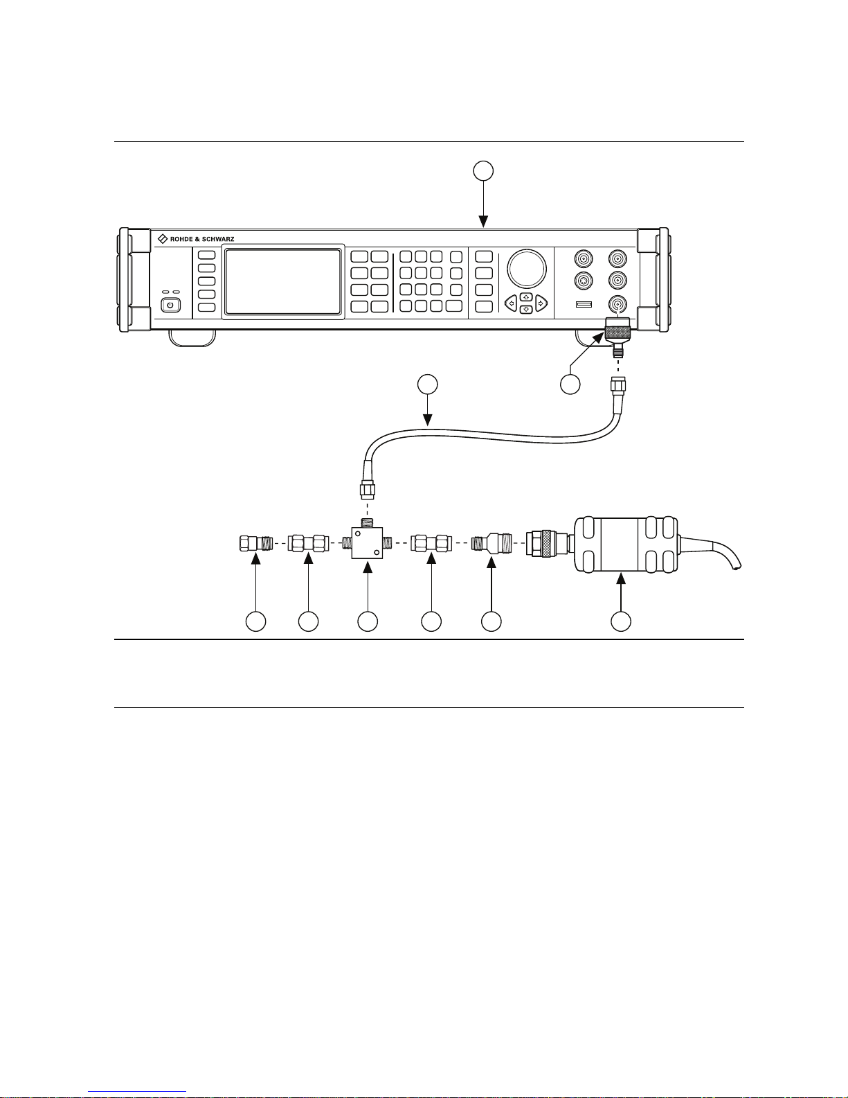
The following figure illustrates the hardware setup.
Figure 1. Connection Diagram for Measuring at Splitter Output 2 (SMA)
8. Configure the signal generator to generate a sine waveform with the following
characteristics:
• Frequency: the Test Point Frequency value from Table 2
• Amplitude level: the Test Point Amplitude value from Table 2
9. Configure the power sensor to correct for the Test Point Frequency value using the power
sensor frequency correction function.
10. Use the power sensor to measure the power in dBm.
11. Repeat steps 8 through 10 for each configuration in Table 2, recording each result as
splitter output 2 power, where each configuration has a corresponding value.
12. Disconnect the power sensor and 50 Ω SMA terminator (f) from splitter output 2 and
splitter output 1.
1 Signal Generator
2 SMA (f)-to-N (m) Adapter
3 SMA (m)-to-SMA (m) Cable
4 50 ΩSMA Terminator (f)
5 SMA (m)-to-SMA (m) Adapter
6 Power Splitter
7 SMA (f)-to-N (f) Adapter
8 Power Sensor
1
64 5
3
7
8
2
5
Page 10

10 | ni.com | PXIe-5185/5186 Calibration Procedure
13. Connect the power sensor to splitter output 1.
14. Connect the 50 Ω SMA terminator (f) to splitter output 2.
The following figure illustrates the hardware setup.
Figure 2. Connection Diagram for Measuring at Splitter Output 1 (SMA)
15. Configure the signal generator to generate a sine waveform with the following
characteristics:
• Frequency: the Test Point Frequency value from Table 2
• Amplitude level: the Test Point Amplitude value from Table 2
16. Configure the power sensor to correct for the Test Point Frequency value using the power
sensor frequency correction function.
17. Use the power sensor to measure the power in dBm.
1 Signal Generator
2 SMA (f)-to-N (m) Adapter
3 SMA (m)-to-SMA (m) Cable
4 Power Sensor
5 SMA (f)-to-N (f) Adapter
6 SMA (m)-to-SMA (m) Adapter
7 Power Splitter
8 50 ΩSMA Terminator
1
3
8
6
7
6
5
4
2
Page 11

PXIe-5185/5186 Calibration Procedure | © National Instruments | 11
18. Repeat steps 15 through 17 for each configuration in Table 2, recording each result as
splitter output 1 power, where each configuration has a corresponding value.
19. Calculate the splitter imbalance for each frequency point using the following equation:
splitter imbalance = splitter output 2 power - splitter output 1 power
20. Disconnect the 50 Ω SMA terminator (f) from splitter output 2. Refer to the remaining
assembly as the power sensor assembly. The power sensor assembly will be used in the
Verifying 50 Ω AC Amplitude Accuracy and Bandwidth procedure.
BNC Adapters
This procedure characterizes the power splitter imbalance when using BNC adapters. The results
of this characterization are later used as a correction in the Verifying 1 MΩ AC Amplitude
Accuracy and Bandwidth procedure.
1. Connect the BNC (f)-to-N (f) adapter to the power sensor. Refer to this assembly as the
power sensor.
2. Zero the power sensor as described in the Zeroing the Power Sensor section.
3. Connect the RF OUT connector of the signal generator to the input port of the power splitter
using an SMA (f)-to-N (m) adapter and an SMA (m)-to-SMA (m) cable.
4. Connect an SMA (m)-to-BNC (m) adapter to one of the power splitter output ports. Refer
to this assembly as splitter output 1.
5. Connect the 50 Ω BNC terminator (f) to splitter output 1.
6. Connect the other SMA (m)-to-BNC (m) adapter to the other output port of the power
splitter. Refer to this assembly as splitter output 2.
Table 3. Power Splitter Characterization with BNC Configuration
Configuration
Test Point
Impedance Frequency (MHz) Amplitude (dBm)
1 1 MΩ 0.05 -0.5
2 1 MΩ 425 -0.5
Page 12

12 | ni.com | PXIe-5185/5186 Calibration Procedure
7. Connect the power sensor to splitter output 2.
The following figure illustrates the hardware setup.
Figure 3. Connection Diagram for Measuring at Splitter Output 2 (BNC)
8. Configure the signal generator to generate a sine waveform with the following
characteristics:
• Frequency: the Test Point Frequency value from Table 3
• Amplitude level: the Test Point Amplitude value from Table 3
9. Configure the power sensor to correct for the Test Point Frequency value using the power
sensor frequency correction function.
10. Use the power sensor to measure the power in dBm.
11. Repeat steps 8 through 10 for each configuration in Table 3, recording each result as
splitter output 2 power, where each configuration has a corresponding value.
12. Disconnect the power sensor and 50 Ω BNC terminator (f) from splitter output 2 and
splitter output 1.
1 Signal Generator
2 SMA (f)-to-N (m) Adapter
3 SMA (m)-to-SMA (m) Cable
4 50 ΩBNC Terminator
5 SMA (m)-to-BNC (m) Adapter
6 Power Splitter
7 BNC (f)-to-N (f) Adapter
8 Power Sensor
1
64 5
3
7
8
2
5
Page 13

PXIe-5185/5186 Calibration Procedure | © National Instruments | 13
13. Connect the power sensor to splitter output 1.
14. Connect the 50 Ω BNC terminator (f) to splitter output 2.
The following figure illustrates the hardware setup.
Figure 4. Connection Diagram for Measuring at Splitter Output 1 (BNC)
15. Configure the signal generator to generate a sine waveform with the following
characteristics:
• Frequency: the Test Point Frequency value from Table 3
• Amplitude level: the Test Point Amplitude value from Table 3
16. Configure the power sensor to correct for the Test Point Frequency value using the power
sensor frequency correction function.
17. Use the power sensor to measure the power in dBm.
18. Repeat steps 15 through 17 for each configuration in Table 3, recording each result as
splitter output 1 power, where each configuration has a corresponding value.
1 Signal Generator
2 SMA (f)-to-N (m) Adapter
3 SMA (m)-to-SMA (m) Cable
4 Power Sensor
5 BNC (f)-to-N (f) Adapter
6 SMA (m)-to-BNC (m) Adapter
7 Power Splitter
8 50 ΩBNC Terminator
1
3
8
6
7
6
5
4
2
Page 14

14 | ni.com | PXIe-5185/5186 Calibration Procedure
19. Calculate the splitter imbalance for each frequency point using the following equation:
splitter imbalance = splitter output 2 power - splitter output 1 power
20. Disconnect the 50 Ω BNC terminator (f) from splitter output 2. Refer to the remaining
assembly as the power sensor assembly. The power sensor assembly will be used in the
Verifying 1 MΩ AC Amplitude Accuracy and Bandwidth procedure.
Verification
This section provides instructions for verifying the PXIe-5185/5186 specifications. Refer to
Table 4 for a list of the verification tests and the equipment needed for each test.
Verifying DC and Programmable Vertical Offset Accuracy
To verify the DC and programmable vertical offset accuracy of the PXIe-5185/5186, compare
the voltage measured by the device and the value sourced by the voltage standard. Table 5 lists
the settings for each channel.
1. Connect the calibrator test head directly to the channel 0, 50 Ω input of the
PXIe-5185/5186.
2. Configure the PXIe-5185/5186 with the following settings:
• Vertical coupling: DC
Table 4. Verification Tests
Test Type
Specification
Recommended
Equipment
50 Ω 1 MΩ
DC Accuracy ±(2% of Input +
0.35% FS +
0.7 mV)
±1.2% of Offset
Setting
±(2% of Input +
0.9% FS + 1.3 mV)
±1.2% of Offset
Setting
Fluke 9500B
Fluke 9530
AC Amplitude
Accuracy
±0.35 dB ±0.5 dB Rohde & Schwarz
SMA100A
Rohde & Schwarz
NRP-Z91
Bandwidth (-3 dB) 3 GHz
(PXIe-5185)
5 GHz
(PXIe-5186)
425 MHz Rohde & Schwarz
SMA100A
Rohde & Schwarz
NRP-Z91
Timebase
Accuracy
±25 ppm Fluke 9500B
Fluke 9530
*
1 MΩ input available on PXIe-5185 module part number 152962x-0zL and PXIe-5186 module part
number 152961x-0zL, where x is any letter and z is any number.
Page 15

PXIe-5185/5186 Calibration Procedure | © National Instruments | 15
• Input impedance: The Input Impedance value from Table 5 for the current iteration
• Max input frequency:
(PXIe-5185) 3 GHz, (PXIe-5186) 5 GHz
• Programmable vertical offset: The Programmable Vertical Offset value from
Table 4 for the current iteration
• Range: The Vertical Range value from Table 5 for the current iteration
• Sample rate: 12.5 GS/s
• Minimum number of samples: 1,048,567
3. Configure the calibrator output impedance to match that of the PXIe-5185/5186 for the
current iteration listed in Table 5.
4. Configure the calibrator to output the Test Point voltage for the current iteration listed in
Table 5.
5. Enable the calibrator output.
6. Wait 2.5 s for settling, then record the measured voltage.
7. Use the following formula to calculate the voltage difference:
error = V measured - Test Point
8. Compare the error to the Test Limit provided in Table 5.
9. Repeat steps 2-8 for iterations 2 through 16 listed in Table 5.
10. Connect the calibrator test head directly to the channel 1 50 Ω input of the PXIe-5185/5186
and repeat steps 2 through 9.
Note If your module supports 1 MΩ input, follow steps 11 and 12. Otherwise, DC
and programmable vertical offset accuracy has been verified. 1 MΩ input is available
on PXIe-5185 module part number 152962x-0zL and PXIe-5186 module part number
152961x-0zL, where x is any letter and z is any number.
11. Connect the calibrator test head directly to the channel 0, 1 MΩ input of the
PXIe-5185/5186 and repeat steps 2 through 8 for iterations 17 through 44 listed in Table 5.
12. Connect the calibrator test head directly to the channel 1, 1 MΩ input of the
PXIe-5185/5186 and repeat steps 2 through 8 for iterations 17 through 44 listed in Table 5.
Table 5. PXIe-5185/5186 DC and Programmable Vertical Offset Accuracy Limits
Iteration
Input
Impedance
Vertical
Range
(V
pk-pk
)
Programmable
Vertical
Offset (V)
Test
Point (V)
Test Limit
(V)
1 50 Ω 0.11 0 0.045 ±0.0020
2 50 Ω 0.11 0 -0.045 ±0.0020
3 50 Ω 0.11 0.25 0.295 ±0.0100
4 50 Ω 0.11 -0.25 -0.295 ±0.0100
Page 16

16 | ni.com | PXIe-5185/5186 Calibration Procedure
5 50 Ω 0.2 0 0.08 ±0.0030
6 50 Ω 0.2 0 -0.08 ±0.0030
7 50 Ω 0.2 0.25 0.33 ±0.0110
8 50 Ω 0.2 -0.25 -0.33 ±0.0110
9 50 Ω 0.5 0 0.2 ±0.0065
10 50 Ω 0.5 0 -0.2 ±0.0065
11 50 Ω 0.5 0.25 0.45 ±0.0145
12 50 Ω 0.5 -0.25 -0.45 ±0.0145
13 50 Ω 1 0 0.4 ±0.0122
14 50 Ω 1 0 -0.4 ±0.0122
15 50 Ω 1 0.25 0.65 ±0.0202
16 50 Ω 1 -0.25 -0.65 ±0.0202
17 1 MΩ 0.11 0 0.045 ±0.0032
18 1 MΩ 0.11 0 -0.045 ±0.0032
19 1 MΩ 0.11 0.25 0.295 ±0.0112
20 1 MΩ 0.11 -0.25 -0.295 ±0.0112
21 1 MΩ 0.2 0 0.08 ±0.0047
22 1 MΩ 0.2 0 -0.08 ±0.0047
23 1 MΩ 0.2 0.25 0.33 ±0.0127
24 1 MΩ 0.2 -0.25 -0.33 ±0.0127
25 1 MΩ 0.5 0 0.2 ±0.0098
26 1 MΩ 0.5 0 -0.2 ±0.0098
27 1 MΩ 0.5 0.25 0.45 ±0.0178
28 1 MΩ 0.5 -0.25 -0.45 ±0.0178
29 1 MΩ 1 0 0.4 ±0.0183
30 1 MΩ 1 0 -0.4 ±0.0183
Table 5. PXIe-5185/5186 DC and Programmable Vertical Offset Accuracy Limits
Iteration
Input
Impedance
Vertical
Range
(V
pk-pk
)
Programmable
Vertical
Offset (V)
Test
Point (V)
Test Limit
(V)
Page 17

PXIe-5185/5186 Calibration Procedure | © National Instruments | 17
Verifying 50 Ω AC Amplitude Accuracy and Bandwidth
Follow this procedure to verify the 50 Ω AC amplitude accuracy and analog bandwidth of the
PXIe-5185/5186 by generating a sine wave and comparing the amplitude measured by the
PXIe-5185/5186 to the amplitude measured by the power sensor.
Before performing this procedure, complete the Test System Characterization procedures and
calculate the splitter imbalance of your power splitter.
Table 6. 50 Ω AC Amplitude Accuracy and Bandwidth Verification
1. Connect splitter output 2 of the power sensor assembly from the Test System
Characterization section to the channel 0, 50 Ω input of the PXIe-5185/5186.
31 1 MΩ 1 0.25 0.65 ±0.0263
32 1 MΩ 1 -0.25 -0.65 ±0.0263
33 1 MΩ 2 0 0.8 ±0.0353
34 1 MΩ 2 0 -0.8 ±0.0353
35 1 MΩ 2 2.5 3.3 ±0.1153
36 1 MΩ 2 -2.5 -3.3 ±0.1153
37 1 MΩ 5 0 2 ±0.0863
38 1 MΩ 5 0 -2 ±0.0863
39 1 MΩ 5 2.5 4.5 ±0.1663
40 1 MΩ 5 -2.5 -4.5 ±0.1663
41 1 MΩ 10 0 4 ±0.1713
42 1 MΩ 10 0 -4 ±0.1713
43 1 MΩ 10 2.5 6.5 ±0.2513
44 1 MΩ 10 -2.5 -6.5 ±0.2513
Iteration Sample Rate Test Point (dBm) Test Limit (dB)
1 1.25 GS/s -12 at 50 kHz ±0.35
2 12.5 GS/s (PXIe-5185) -12 at 3 GHz
(PXIe-5186) -12 at 5 GHz
-3 to 1
Table 5. PXIe-5185/5186 DC and Programmable Vertical Offset Accuracy Limits
Iteration
Input
Impedance
Vertical
Range
(V
pk-pk
)
Programmable
Vertical
Offset (V)
Test
Point (V)
Test Limit
(V)
Page 18

18 | ni.com | PXIe-5185/5186 Calibration Procedure
Note The power sensor assembly must match the configuration used in the Test
System Characterization section, in which the power sensor is connected to splitter
output 1 and the signal generator is connected to the input port of the power splitter.
The following figure illustrates the hardware setup.
Figure 5. 50 Ω AC Amplitude Accuracy and Bandwidth Verification Cabling Diagram
1 Power Sensor
2 SMA (f)-to-N(f) Adapter
3 SMA (m)-to-SMA (m) Adapter
4 Power Splitter
5 PXIe-5185/5186
6 SMA (m)-to-SMA (m) Cable
7 SMA (f)-to-N (m) Adapter
8 Signal Generator
3 GHz 12.5 GS/s 8-Bit Digitizer
ACCESS
ACTIVE
REF CLK
CLK IN
+16 dBm Max
(1.4 Vrms)
50˖
+9 dBm Max
(0.6 Vrms)
50˖
1 Vpp measure
± 1 V MAX
1 Vpp measure
± 1 V MAX
10 Vpp measure
± 42 V MAX
10 Vpp measure
± 42 V MAX
CH 0
CH 1
TRIG
ESD
SENSITIVE
NI PXIe-5185
50˖
1M˖
50˖
1M˖
50˖
± 5 V
MAX
6
5
8
7
2
1
3
4
3
Page 19

PXIe-5185/5186 Calibration Procedure | © National Instruments | 19
2. Configure the PXIe-5185/5186 with the following settings:
• Vertical coupling: DC
• Input impedance: 50 Ω
• Maximum input frequency: 3 GHz (PXIe-5185), 5 GHz (PXIe-5186)
• Range: 0.11 V
pk-pk
• Sample rate: The Sample Rate value from Table 6 for the current iteration
• Minimum number of samples: 1,048,567
3. Configure the signal generator to generate a sine waveform with the following
characteristics:
• Frequency: the Test Point frequency value from Table 6
• Amplitude level: the Test Point amplitude value from Table 6
4. Configure the power sensor to correct for the Test Point frequency using the power sensor
frequency correction function.
5. Use the power sensor to measure the power in dBm. Record the result as measured input
power.
6. Calculate the corrected input power using the following equation:
corrected input power = measured input power + splitter imbalance
Note Select the splitter imbalance value from the list of test points from the Test
System Characterization section for the current Test Point frequency from Table 6.
7. Use the PXIe-5185/5186 to acquire and measure the power using the Extract Single Tone
Information VI, converting the result from Vpk to dBm. Record the result as device input
power.
8. If the Test Point frequency from Table 6 is 50 kHz, proceed to the following step.
Otherwise, go to step 12.
9. Calculate the power reference using the following equation:
power reference = device input power - corrected input power
10. Compare the power reference to the test limit for Iteration 1 in Table 6 to verify the 50 Ω
AC amplitude accuracy.
11. Go to step 14. The power error is not calculated for this configuration.
12. Calculate the power error using the following equation:
power error = device input power - corrected input power - power reference
13. Compare the power error to the test limit for Iteration 2 in Table 6 to verify the 50 Ω analog
bandwidth.
14. Repeat steps 2 through 13 for each Iteration in Table 6.
15. Connect splitter output 2 of the power sensor assembly to the channel 1 50 Ω input of the
PXIe-5185/5186 and repeat steps 2 through 13 for each Iteration listed in Table 6.
Page 20

20 | ni.com | PXIe-5185/5186 Calibration Procedure
Verifying 1 MΩAC Amplitude Accuracy and Bandwidth
Follow this procedure to verify the 1 MΩ AC amplitude accuracy and analog bandwidth of the
PXIe-5185/5186 by generating a sine wave and comparing the amplitude measured by the
PXIe-5185/5186 to the amplitude measured by the power sensor.
Before performing this procedure, complete the Test System Characterization procedures and
calculate the splitter imbalance of your power splitter.
1. Connect the 50 Ω BNC feed-through terminator to the channel 0 1 MΩ input of the
PXIe-5185/5186. Connect splitter output 2 of the power sensor assembly from the Test
System Characterization section to the 50 Ω BNC feed-through terminator.
Note The power sensor assembly must match the configuration used in the Test
System Characterization section, in which the power sensor is connected to splitter
output 1 and the signal generator is connected to the input port of the power splitter.
Table 7. 1 MΩ AC Amplitude Accuracy and Bandwidth Verification
Iteration Sample Rate Test Point (dBm) Test Limit (dB)
1 1.25 GS/s -12 at 50 kHz ±0.5
2 12.5 GS/s -12 at 425 MHz -3 to 1
Page 21

PXIe-5185/5186 Calibration Procedure | © National Instruments | 21
The following figure illustrates the hardware setup.
Figure 6. 1 MΩ AC Amplitude Accuracy and Bandwidth Verification Cabling Diagram
2. Configure the PXIe-5185/5186 with the following settings:
• Vertical coupling: DC
• Input impedance: 1 MΩ
1 Power Sensor
2 BNC (m)-to-N (m) Adapter
3 SMA (f)-to-BNC (f) Adapter
4 Power Splitter
5 50 ΩBNC Feed-Through
6 PXIe-5185/5186
7 SMA (f)-to-SMA (f) Cable
8 SMA (m)-to-N (f) Adapter
9 Signal Generator
3 GHz 12.5 GS/s 8-Bit Digitizer
ACCESS
ACTIVE
REF CLK
CLK IN
+16 dBm Max
(1.4 Vrms)
50˖
+9 dBm Max
(0.6 Vrms)
50˖
1 Vpp measure
± 1 V MAX
1 Vpp measure
± 1 V MAX
10 Vpp measure
± 42 V MAX
10 Vpp measure
± 42 V MAX
CH 0
CH 1
TRIG
ESD
SENSITIVE
NI PXIe-5185
50˖
1M˖
50˖
1M˖
50˖
± 5 V
MAX
7
6
9
8
2
1
3
4
5
3
Page 22

22 | ni.com | PXIe-5185/5186 Calibration Procedure
• Maximum input frequency: 425 MHz
• Range: 0.11 V
pk-pk
• Sample rate: The Sample Rate value from Table 7 for the current iteration
• Minimum number of samples: 1,048,567
3. Configure the signal generator to generate a sine waveform with the following
characteristics:
• Frequency: the Test Point frequency from Table 7
• Amplitude level: the Test Point amplitude from Table 7
4. Configure the power sensor to correct for the Test Point frequency using the power sensor
frequency correction function.
5. Use the power sensor to measure the power in dBm. Record the result as measured input
power.
6. Calculate the corrected input power using the following equation:
corrected input power = measured input power + splitter imbalance
Note Select the splitter imbalance value from the list of test points from the Test
System Characterization section for the current Test Point frequency from Table 7.
7. Use the PXIe-5185/5186 to acquire and measure the power using the Extract Single Tone
Information VI, converting the result from Vpk to dBm. Record the result as device input
power.
8. If the Test Point frequency from Table 7 is 50 kHz, proceed to step 9. Otherwise, go to
step 12.
9. Calculate the power reference using the following equation:
power reference = device input power - corrected input power
10. Compare the power reference to the test limit for Iteration 1 in Table 7 to verify the 1 MΩ
AC amplitude accuracy.
11. Go to step 14. The power error is not calculated for this configuration.
12. Calculate the power error using the following equation:
power error = device input power - corrected input power - power reference
13. Compare the power error to the test limit for Interation 2 in Table 7 to verify the 1 MΩ
analog bandwidth.
14. Repeat steps 2 through 13 for each Iteration in Table 7.
15. Connect the 50 Ω BNC feed-through terminator to the channel 1 1 MΩ input of the
PXIe-5185/5186. Connect splitter output 2 of the power sensor assembly to the 50 Ω BNC
feed-through terminator and repeat steps 2 through 13 for each Iteration in Table 7.
Page 23

PXIe-5185/5186 Calibration Procedure | © National Instruments | 23
Verifying Timebase Accuracy
To verify the timebase accuracy of the PXIe-5185/5186 compare the peak frequency of a leveled
sine wave measured by the PXIe-5185/5186 and the value sourced by the calibrator. Table 8 lists
the settings.
1. Configure the PXIe-5185/5186 with the following settings:
• Vertical coupling: DC
• Input impedance: 50 Ω
• Max input frequency:
(PXIe-5185) 3 GHz, (PXIe-5186) 5 GHz
• Range: 1 V
pk-pk
• Sample rate: 12.5 GS/s
• Minimum number of samples: 1,048,567
2. Connect the calibrator test head directly to the channel 0, 50 Ω input of the digitizer.
3. Configure the calibrator output impedance to 50 Ω .
4. Configure the calibrator to output a 1.0 GHz leveled sine wave with peak-to-peak voltage
amplitude of 0.90 V.
5. Enable the calibrator output.
6. Wait 2.5 s for settling, then record the measured peak frequency.
7. Use the following formula to calculate the frequency difference:
TBerror = ( f - 1.0E+9)/1.0E+3
where f = measured frequency
8. Compare the error to the Test Limit shown in Table 8.
Note Timebase verification is only required on one channel.
Adjustment
If the PXIe-5185/5186 successfully passed each of the verification procedures within the test
limits, then an adjustment is recommended but not required to warrant the published
specifications for the next year. If the digitizer was not within the test limits for each of the
verification procedures, you can perform the adjustment procedure to improve the accuracy of
the digitizer.
An adjustment is required once a year. Following the adjustment procedure automatically
updates the calibration date and temperature in the EEPROM of the digitizer.
Table 8. PXIe-5185/5186 Timebase Accuracy Limits
Channel Function
Input
Impedance
Range
(V
pk-pk
)
Test Point
(V
pk-pk
) Test Limit
0 Timebase 50 Ω 1.0 0.9 at 1 GHz ±25 ppm
(25.0 kHz)
Page 24

24 | ni.com | PXIe-5185/5186 Calibration Procedure
Complete the following steps to externally adjust the PXIe-5185/5186.
1. Obtain a calibration session handle using the niScope Cal Start VI.
2. Connect the calibrator test head directly to the channel 0, 50 Ω input of the digitizer.
3. Configure the calibrator output impedance to 50 Ω.
4. Configure the calibrator to output the voltage listed under Input (V) in Table 9 for the
current iteration.
5. Enable the calibrator output.
6. Wait 2.5 s for the impedance matching of the calibrator to settle.
7. Adjust the vertical range using the niScope Cal Adjust Range VI.
8. Repeat steps 4 through 7 for each iteration in Table 9.
9. Connect the calibrator test head directly to the channel 1, 50 Ω input of the digitizer and
repeat steps 3 through 8, changing the value of the channels parameter from
"0" to "1".
Note If your module supports 1 MΩ input, follow steps 10 through 22. Otherwise,
jump to step 23 to complete the adjustment. 1 MΩ input available on PXIe-5185
module part number 152962X-0ZL and PXIe-5186 module part number
152961X-0ZL, where X is any letter and Z is any number.
10. Connect the calibrator test head directly to the channel 0, 1 MΩ input of the digitizer.
11. Configure the calibrator output impedance to 1 MΩ.
12. Configure the calibrator to output a 100 kHz symmetrical square wave with peak-to-peak
voltage amplitude of 8.0 V.
LabVIEW VI C/C++ Function Call
Call niScope_CalStart with the
following parameters:
resourceName: The device number
assigned by MAX
password:
"NI"
LabVIEW VI C/C++ Function Call
Call niScope_CalAdjustRange with
the following parameters:
vi: The instrument handle from
niScope_CalStart
channelName: "0"
range: 0
stimulus: The Input (V) value listed in
Table 9 for the current iteration
Page 25

PXIe-5185/5186 Calibration Procedure | © National Instruments | 25
13. Enable the calibrator output.
14. Wait 2.5 s for the impedance matching of the calibrator to settle.
15. Adjust the 1 MΩ compensation attenuator using the niScope Cal Adjust Compensation
Attenuator VI.
16. Configure the calibrator output impedance to 1 MΩ.
17. Configure the calibrator to output the voltage listed under Input (V) in Table 10 for the
current iteration.
18. Enable the calibrator output.
19. Wait 2.5 s for the impedance matching of the calibrator to settle.
20. Adjust the vertical range using the niScope Cal Adjust Range VI.
21. Repeat steps 17 through 20 for each iteration in Table 10.
22. Connect the calibrator test head directly to the channel 1, 1 MΩ input of the digitizer and
repeat steps 11 through 21, changing the value of the channels parameter from
"0" to "1".
23. Connect the calibrator test head directly to the external trigger channel input on the
digitizer.
24. Configure the calibrator output impedance to 50 Ω.
25. Configure the calibrator to output the voltage listed under Input (V) in Table 11 for the
current iteration. Configure the load impedance of the calibrator to 50 Ω.
26. Enable the calibrator output.
LabVIEW VI C/C++ Function Call
Call
niScope_CalAdjustCompensatio
nAttenuator
with the following
parameters:
vi: The instrument handle from
niScope_CalStart
channelName: "0"
range: 8.0
LabVIEW VI C/C++ Function Call
Call niScope_CalAdjustRange with
the following parameters:
vi: The instrument handle from
niScope_CalStart
channelName: "0"
range: 0
stimulus: The Input (V) value listed in
Table 10 for the current iteration
Page 26

26 | ni.com | PXIe-5185/5186 Calibration Procedure
27. Wait 2.5 s for the impedance matching of the calibrator to settle.
28. Adjust the vertical range using the niScope Cal Adjust Range VI.
.
29. Repeat steps 25 through 28 for each iteration in Table 11.
30. Disconnect or disable all inputs to the digitizer.
31. Self-calibrate the digitizer using niScope Cal Self Calibrate VI.
32. End the calibration session by calling the niScope Cal End VI.
You have finished adjusting the PXIe-5185/5186. Repeat the Verification section to reverify the
performance of the digitizer after adjustments.
LabVIEW VI C/C++ Function Call
Call niScope_CalAdjustRange with
the following parameters:
vi: The instrument handle from
niScope_CalStart
channelName:
"NISCOPE_VAL_EXTERNAL"
range: 0
stimulus: The Input (V) value listed in
Table 11 for the current iteration
LabVIEW VI C/C++ Function Call
Call niScope_CalSelfCalibrate
with the following parameters:
vi: The instrument handle from
niScope_CalStart
channelList: VI_NULL
option: VI_NULL
LabVIEW VI C/C++ Function Call
Call niScope_CalEnd with the
following parameters:
sessionHandle: The instrument handle
from
niScope_CalStart
action:
NISCOPE_VAL_ACTION_STORE to
save the results of the calibration
Page 27

PXIe-5185/5186 Calibration Procedure | © National Instruments | 27
Table 9. PXIe-5185/5186 50 Ω Input Parameters for Input Channel
External Adjustment
Iteration Input (V)
1 0.32
2 0.135
3 0.075
4 0.065
5 0.055
6 0.045
7 -0.045
8 -0.055
9 -0.065
10 -0.075
11 -0.135
12 -0.32
13 2.0
14 -2.0
Table 10. PXIe-5185/5186 1 MΩ Input Parameters for Input Channel
External Adjustment
Iteration Input (V)
1 5.0
2 3.0
3 2.0
4 1.0
5 0.75
6 0.5
7 0.32
8 0.135
9 0.075
Page 28

28 | ni.com | PXIe-5185/5186 Calibration Procedure
10 0.065
11 0.055
12 0.045
13 -0.045
14 -0.055
15 -0.065
16 -0.075
17 -0.135
18 -0.32
19 -0.5
20 -0.75
21 -1.0
22 -2.0
23 -3.0
24 -5.0
Table 11. PXIe-5185/5186 Input Parameters for External Trigger Channel
External Adjustment
Iteration Input (V)
1 -5.0
2 0.001
3 5.0
Table 10. PXIe-5185/5186 1 MΩ Input Parameters for Input Channel
External Adjustment (Continued)
Iteration Input (V)
Page 29

© 2011–2018 National Instruments. All rights reserved.
373258F-01
April 24, 2018
Information is subject to change without notice. Refer to the NI Trademarks and Logo Guidelines atni.com/trademarks for more
information on NI trademarks. Other product and company names mentioned herein are trademarks or trade names of their
respective companies. For patents covering NI products/technology, refer to the appropriate location: Help»Patents in your
software, the
patents.txt file on your media, or the National Instruments Patents Notice at ni.com/patents. You can find
information about end-user license agreements (EULAs) and third-party legal notices in the readme file for your NI product. Refer
to the Export Compliance Information at
ni.com/legal/export-compliance for the NI global trade compliance policy and how
to obtain relevant HTS codes, ECCNs, and other import/export data. NI MAKES NO EXPRESS OR IMPLIED WARRANTIES AS
TO THE ACCURACY OF THE INFORMATION CONTAINED HEREIN AND SHALL NOT BE LIABLE FOR ANY ERRORS. U.S.
Government Customers: The data contained in this manual was developed at private expense and is subject to the applicable
limited rights and restricted data rights as set forth in FAR 52.227-14, DFAR 252.227-7014, and DFAR 252.227-7015.
Worldwide Support and Services
The NI website is your complete resource for technical support. At ni.com/support you have
access to everything from troubleshooting and application development self-help resources to
email and phone assistance from NI Application Engineers.
Visit
ni.com/services for NI Factory Installation Services, repairs, extended warranty, and
other services.
Visit
ni.com/register to register your NI product. Product registration facilitates technical
support and ensures that you receive important information updates from NI.
A Declaration of Conformity (DoC) is our claim of compliance with the Council of the European
Communities using the manufacturer’s declaration of conformity. This system affords the user
protection for electromagnetic compatibility (EMC) and product safety. You can obtain the DoC
for your product by visiting
ni.com/certification. If your product supports calibration,
you can obtain the calibration certificate for your product at
ni.com/calibration.
NI corporate headquarters is located at 11500 North Mopac Expressway, Austin, Texas,
78759-3504. NI also has offices located around the world. For telephone support in the United
States, create your service request at
ni.com/support or dial 1 866 ASK MYNI (275 6964).
For telephone support outside the United States, visit the Worldwide Offices section of
ni.com/niglobal to access the branch office websites, which provide up-to-date contact
information, support phone numbers, email addresses, and current events.
 Loading...