

Page 1

CALIBRATION PROCEDURE
PXIe-4330/4331
This document contains information about verifying and adjusting National Instruments
PXIe-4330/4331 modules using NI-DAQmx 9.1 and later. For more information about
calibration, visit
Contents
Software.................................................................................................................................... 2
Documentation.......................................................................................................................... 2
Calibration Interval................................................................................................................... 2
Test Equipment......................................................................................................................... 3
Test Conditions......................................................................................................................... 4
Calibration Procedure ............................................................................................................... 4
Initial Setup....................................................................................................................... 5
Connecting the Equipment ............................................................................................... 5
Verification Procedures .................................................................................................... 11
Gain and Offset Adjustment Procedure............................................................................ 20
Test Limits................................................................................................................................ 24
Gain Accuracy Test Limits............................................................................................... 25
Input Offset Test Limits ................................................................................................... 31
Shunt Quarter-Bridge Calibration Test Limits ................................................................. 32
Shunt Calibration Resistance Test Limits ........................................................................ 32
Excitation Voltage Test Limits......................................................................................... 33
Appendix A: Connection Path Details...................................................................................... 34
Worldwide Support and Services ............................................................................................. 40
ni.com/calibration.
Install the CAL-4330 Into a Rack (Optional)........................................................... 7
Connect the Calibration and Switch Cables ............................................................. 8
Connect the DMM and Multifunction Calibrator Cables......................................... 10
Gain Accuracy Verification...................................................................................... 11
Input Offset Verification .......................................................................................... 14
Shunt Quarter-Bridge Calibration Accuracy Verification........................................ 15
Shunt Calibration Resistance Accuracy Verification ............................................... 17
Excitation Voltage Verification................................................................................ 18
Page 2

Software
Install NI-DAQmx 9.1 or later on the calibration computer. NI-DAQmx includes high-level
function calls to simplify the task of writing software to calibrate modules. You must have the
proper module driver installed on the calibration system before calibrating the module.
Note NI recommends that you install the NI-DAQmx driver software before
physically installing the PXIe-4330/4331. NI-DAQmx, available at
downloads
, configures and controls the PXIe-4330/4331.
ni.com/
NI-DAQmx supports a number of programming languages, including LabVIEW,
LabWindows
™
/CVI™, C/C++, C#, and Visual Basic .NET.
Documentation
The following documents are your primary references for writing your calibration utility with
NI-DAQmx. You can download the latest version of these documents from the NI Web site at
ni.com/manuals.
•The NI SC Express 4330/4331 Installation Guide and Terminal Block Specifications
provides instructions for installing and configuring the NI PXIe-4330/4331 module.
•The NI PXIe-4330/4331 User Manual describes how to use the NI PXIe-4330/4331.
•The NI PXIe-4330/4331 Specifications lists the specifications for the NI PXIe-4330/4331.
•The NI-DAQmx Help includes information about creating applications that use the
NI-DAQmx driver.
•The NI-DAQmx C Reference Help includes information about the functions in the driver.
Calibration Interval
National Instruments recommends a calibration interval of one year for the PXIe-4330/4331.
Adjust and verify the PXIe-4330/4331 at the recommended calibration interval based on the
measurement accuracy demands of your application.
2 | ni.com | PXIe-4330/4331 Calibration Procedure
Page 3

Test Equipment
National Instruments recommends that you use the equipment in Table 1 for calibrating an
PXIe-4330/4331 module.
Table 1. Recommended Equipment
Equipment Recommended Model(s) Requirements
Multifunction
calibrator
DMMs (x2) PXI-4071 If this instrument is unavailable, use
Chassis PXIe-1062Q If this chassis is unavailable, use another
Switch modules (x2) PXIe-2737 4x64 2-wire relay module
160-Pin DIN to
160-Pin DIN cable
for PXIe-2737 (x2)
CAL-4330 to
PXIe-4330/4331
calibration cable
Fluke 5520A If this instrument is unavailable, use a
calibrator that can provide resistance values
in the range of 120 Ω to 1 k Ω with 0.01 Ω
resolution, an accuracy of 90 ppm or better,
automatic lead wire compensation, and
2-wire output compensation.
multiranging 6 1/2 digit DMMs with a DC
voltage accuracy of 40 ppm or better of
reading +6 ppm of range for the 10 V and
1 V ranges, and 4-wire resistance
measurement capability with resistance
accuracy of 80 ppm or better of reading
+6 ppm range for the 100 k Ω range
PXIe chassis
NI Part Number: 782417-02 Cable for connecting the PXIe-2737s to the
CAL-4330
NI Part Number: 787003-01 Cable and included standoffs for connecting
the PXIe-4330/4331 DUT to the CAL-4330
Connection
accessory
Banana-to-banana
patch cables (x10)
CAL-4330, NI Part Number
786988-01
Five Pomona 1440-36-0 black
banana plug patch cords
(cables)
Five Pamona 1440-36-1 red
banana plug patch cords
(cables)
PXIe-4330/4331 Calibration Procedure | © National Instruments | 3
Calibration Fixture to enable automated
calibration of the PXIe-4330/4331
—
Page 4

Test Conditions
The following setup and environmental conditions are required to ensure the NI device meets
published specifications.
• Keep connections to the module as short as possible. Long cables and wires act as antennae,
picking up extra noise that can affect measurements.
• Use shielded copper wire for all cable connections to the module. Use twisted-pair wire to
eliminate noise and thermal offsets.
• Maintain an ambient temperature of 23 °C ±5 °C.
• Keep relative humidity below 80%.
• Allow a warm-up time of at least 15 minutes to ensure that the measurement circuitry is at
a stable operating temperature.
• Ensure that the PXI Express chassis fan speed is set to HIGH, that the fan filters are clean,
and that the empty slots contain filler panels. For more information, refer to the Maintain
Forced-Air Cooling Note to Users document available at
• Warm-up time for test equipment may vary depending on the manufacturer. Please refer to
the equipment’s Operators Manual for specified warm-up time.
• To meet Fluke 5520A specifications, zero the Calibrator every 7 days, or when the
Calibrator ambient temperature changes by more than 5 °C. Warm-up time for Fluke 5520A
is 30 minutes.
ni.com/manuals.
Calibration Procedure
This section provides instructions for verifying the performance of the PXIe-4330/4331.
The calibration process consists of the following steps:
1. Initial Setup—Install the module and configure it in Measurement & Automation Explorer
(MAX).
2. Verification Procedures—Verify the existing operation of the module. This step confirms
whether the module is operating within the published specifications—gain accuracy, input
offset, shunt quarter-bridge calibration, shunt calibration resistance, and excitation—prior
to adjustment.
3. Gain and Offset Adjustment Procedure—If necessary, perform an external calibration that
adjusts the module calibration constants with respect to a known calibration source.
4. Reverification—Repeat the verification procedure to ensure that the module is operating
within the published specifications after adjustment.
4 | ni.com | PXIe-4330/4331 Calibration Procedure
Page 5

Initial Setup
You must configure the module in MAX to communicate with NI-DAQmx.
Complete the following steps to configure a module in MAX. Refer to the
NI SC Express 4330/4331 Installation Guide and Terminal Block Specifications for complete
installation instructions.
1. Install the NI-DAQmx, 9.1 or later, driver software.
Caution Always have the PXI Express chassis turned off when inserting a module.
2. Insert the module into an available slot in the PXI Express chassis.
3. Power on the chassis.
4. Launch MAX.
5. Expand Devices and Interfaces to confirm that MAX detects the module.
6. Right-click the module name and select Self-Test to ensure that the module is working
properly.
Note When a module is configured with MAX, it is assigned a module name. Each
function call uses this module name to determine which DAQ module to calibrate.
This document uses
use the module name as it appears in MAX.
Dev1 to refer to the module name. In the following procedures,
Connecting the Equipment
The CAL-4330 and two switch modules provide the ability to programmatically connect the
required module connections as needed for the various verification and calibration steps.
Refer to the specific verification or calibration procedure section for information describing the
required switch connections. Detailed connection paths for each of the verification calibration
steps are shown in Appendix A: Connection Path Details. Before connecting or disconnecting
the calibrator from the module, always set the calibrator to standby mode (STBY).
PXIe-4330/4331 Calibration Procedure | © National Instruments | 5
Page 6
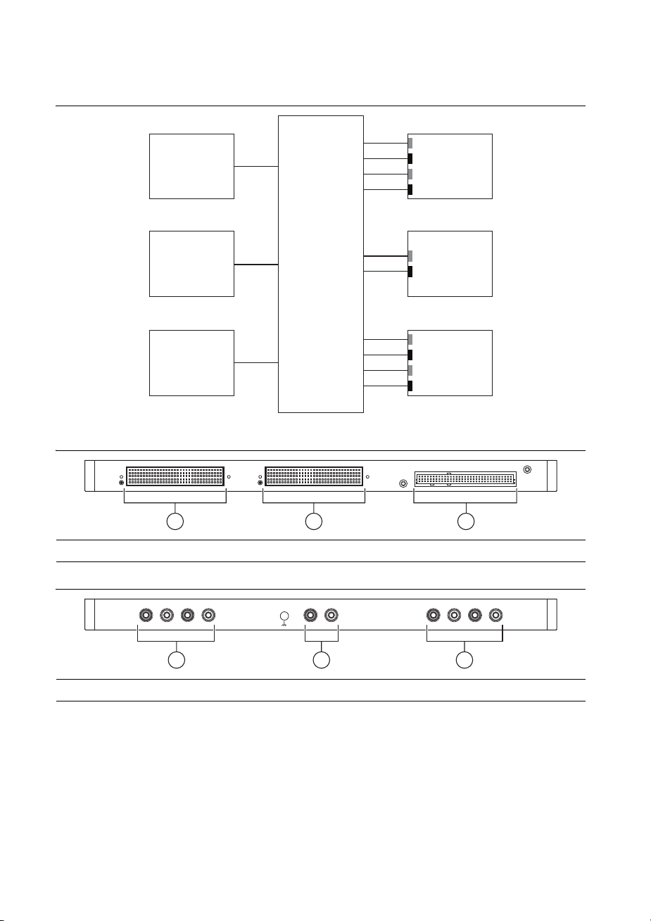
Refer to Figure 1 for a block diagram of the equipment connections. Figure 2 and Figure 3 show
the front and rear connectors on the CAL-4330.
Figure 1. Block Diagram
CAL-4330
SWITCH 1
2-wire
4x64 Switch
SWITCH 2
2-wire
4x64 Switch
DUT
PXIe-4330 or
PXIe 4331
SWITCH 1
1
CAL-4330
Figure 2. Front Connectors
SWITCH 2
2
DMM 2
HI
LO
SENSE HI
SENSE LO
DMM 1
HI
LO
CALIBRATOR
VOLTS HI
VOLTS LO
AUX HI
AUX LO
DEVICE UNDER TEST
PXIe-4330/4331
3
1SWITCH 1 2SWITCH 2 3 DEVICE UNDER TEST
Figure 3. Rear Connectors
CAL-4330
LO HI
VOLTS
LO HI
DMM 2 DMM 1
1
VOLTS
LO HI
2
SENSE
1DMM 2 2DMM 1 3CALIBRATOR
6 | ni.com | PXIe-4330/4331 Calibration Procedure
AUX
LO HI
CALIBRATOR
3
VOLTS
LO HI
Page 7
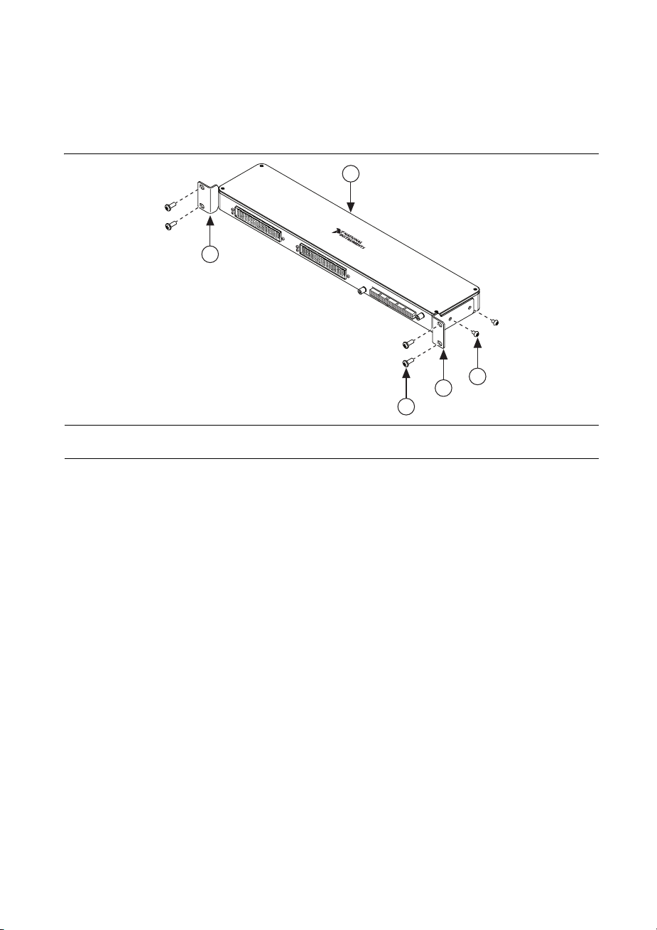
Install the CAL-4330 Into a Rack (Optional)
To install the CAL-4330 into a rack, complete the following steps:
1. Attach the two rack-mount brackets to the sides of the CAL-4330. The brackets and screws
are included with the CAL-4330.
Figure 4. Using the Rack-Mount Brackets
1
CAL-4330
SWITCH 1
S
2
WITCH 2
DEVI
C
E
PXI
UN
e-4330/4331
DE
R T
ES
T
3
2
4
1 CAL-4330
2 Rack-Mount Brackets (2)
3 Rack-Mount Bracket Mounting Screws (4)
4 Rack-Mounting Screws (4)
2. Place the CAL-4330 in the desired position in your rack.
3. Install and tighten the four rack-mounting screws that are included with the CAL-4330.
If the chassis is not already installed in the rack (optional), complete the following steps:
1. Attach the PXIe chassis rack-mount hardware to the PXIe chassis. Refer to your
rack-mount kit installation guide for more details.
2. Mount the PXIe chassis in the rack in the desired position. Refer to your rack-mount kit
installation guide for more details.
PXIe-4330/4331 Calibration Procedure | © National Instruments | 7
Page 8
Connect the Calibration and Switch Cables
NI
P
X
I
e-
10
62Q
C
OOL
I
N
G
C
L
E
A
R
A
N
C
E
A
N
D
FA
N
F
I
L
T
E
R
M
A
I
N
TE
N
A
N
C
E
R
E
Q
U
I
R
E
D.
S
E
E
M
A
N
U
A
L
.
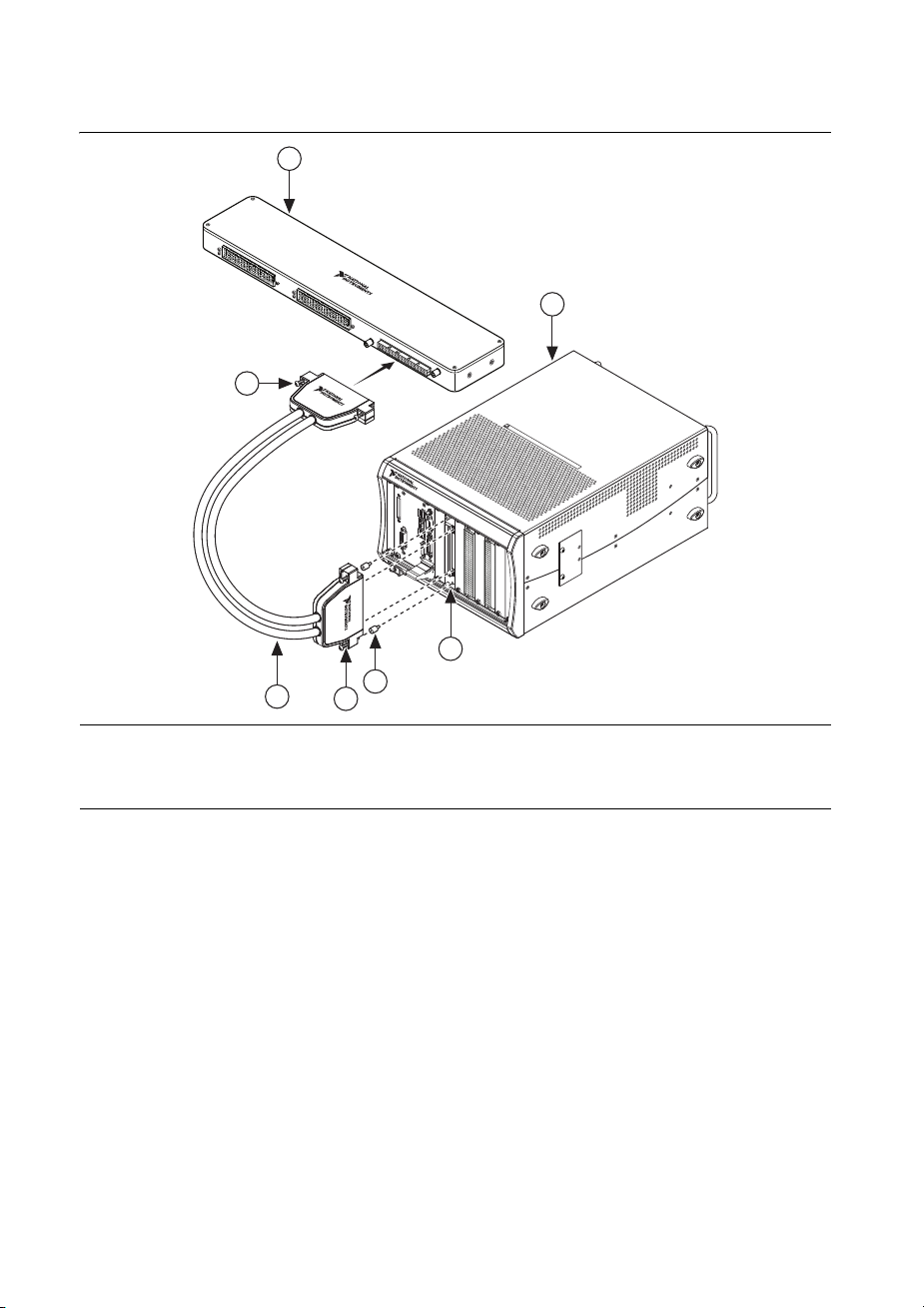
Figure 5. Connecting the Calibration Cable
1
C
A
L
-433
0
S
W
I
TC
H 1
S
W
I
TC
H 2
DE
VI
C
E
PXI
UND
e
4330/4331
E
R
TE
S
T
7
NI
P
3
6
4
5
2
C
O
O
L
I
N
G
C
LE
A
R
A
N
C
E
A
N
D
F
A
N
F
I
L
T
E
R
M
A
I
N
T
E
N
A
N
C
E
R
E
Q
U
I
R
E
D
XI
e-1062Q
.
S
E
E
MA
N
U
A
L.
1CAL-4330
2 PXI Chassis
3 PXIe-4330/4331 (DUT)
5 Jack Screws (2)
6 CAL-4330 to PXIe-4330/4331 Calibration Cable
7 Jack Screws (2)
4 Standoffs (2)
1. Screw the two standoffs into the PXIe-4330/4331 module and tighten the standoffs to
1.30 N · m (11.5 lb · in.), as shown in Figure 5.
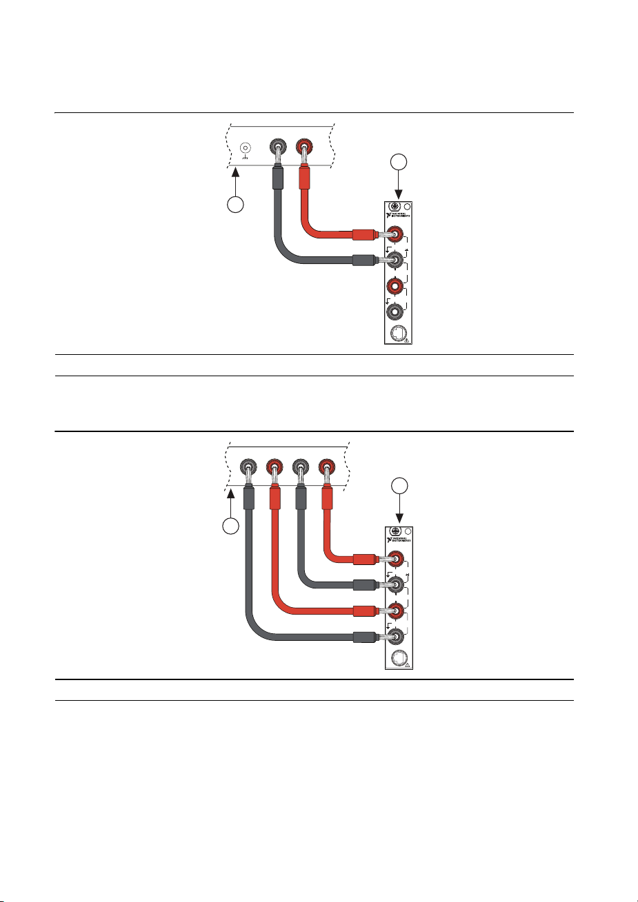
2. Connect the male end of the calibration cable to the CAL-4330 and tighten the two jack
screws to 0.90 N · m (8.0 lb · in.), as shown in Figure 5.
3. Connect the female end of the calibration cable to the PXIe-4330/4331 and tighten the two
jack screws to 0.90 N · m (8.0 lb · in.), as shown in Figure 5.
8 | ni.com | PXIe-4330/4331 Calibration Procedure
Page 9
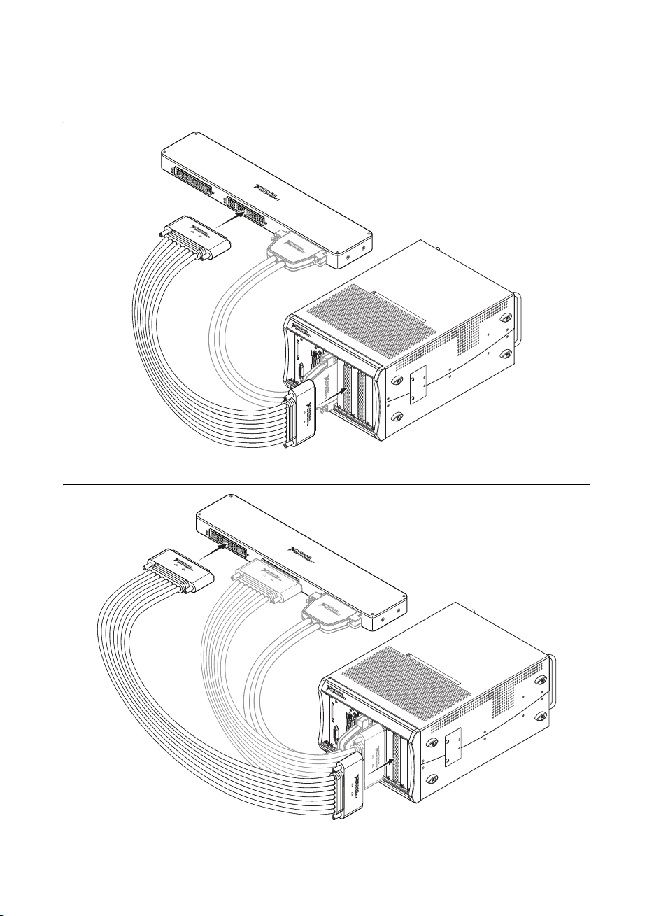
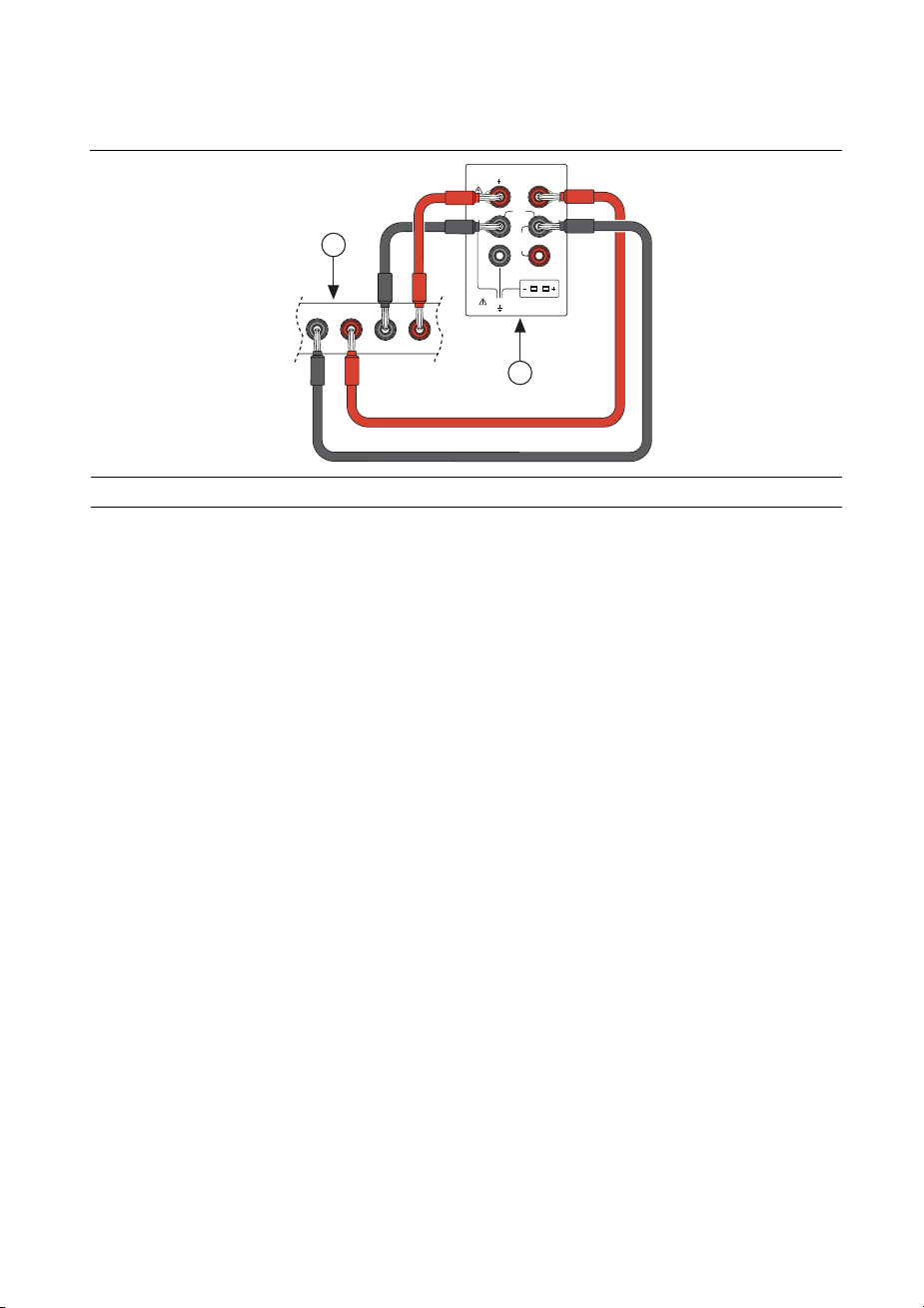
4. Connect the two 160-Pin DIN to 160-Pin DIN cables from the CAL-4330 to the two
N
I
PX
I
e-1
062Q
C
O
O
L
I
N
G
C
L
E
A
R
A
N
C
E
A
N
D
F
A
N
F
I
LT
E
R
M
A
I
N
T
E
N
A
NC
E
R
E
Q
U
I
R
E
D
.
S
E
E
M
A
N
U
A
L
.
150V
1
5
0
V
NI
P
X
I
e
-1
0
62
Q
N
I
P
X
I
e-1
062Q
C
O
O
L
I
NG
C
LE
A
R
A
N
C
E
A
N
D
F
A
N
F
I
LTE
R
MA
I
N
T
E
N
A
N
C
E
R
E
Q
U
I
R
E
D
.
S
E
E
M
A
N
U
A
L
.
C
O
O
L
I
N
G
C
L
E
A
R
A
N
C
E
A
N
D
F
A
N
F
I
LT
E
R
M
A
I
N
TE
N
A
N
C
E
R
E
Q
U
I
R
E
D
.
S
E
E
M
A
N
U
A
L
.
150V150V
1
5
0V
1
5
0V
150V150V
1
5
0
V
1
5
0
V
PXIe-2737 modules and tighten all the jack screws to 0.56 N · m (5.0 lb · in.), as shown in
Figure 6 and Figure 7.
Figure 6. Connecting the Switch 2 Cable
1
5
0
V
CO
O
L
I
N
G
C
LE
A
R
A
N
C
E
A
N
D
F
A
N
F
I
LTE
R
M
A
I
N
T
E
N
A
N
C
E
R
E
Q
U
I
R
E
D
.
S
E
E
M
A
N
U
A
L.
N
I
P
X
I
e
-1
0
62
Q
150V
Figure 7. Connecting the Switch 1 Cable
PXIe-4330/4331 Calibration Procedure | © National Instruments | 9
Page 10
Connect the DMM and Multifunction Calibrator Cables
HI
LO
300 V
MAX
CAT II
HI
LO
AUX I/O
1 A
250 V
MAX
300 V
MAX
CAT II
5 V
MAX
AMPS
INPUT
V
˖
SENSE
˖ 4W
NI PXI-4071
6½-Digit FlexDMM
SENSE
DMM 2
LO HI
VOLTS
LO HI
1
2
1. Connect DMM 1 on the back of the CAL-4330 to a PXI-4071 as shown in Figure 8.
Figure 8. DMM 1
VOLTS
LO HI
DMM 1
2
1
NI PXI-4071
6½-Digit FlexDMM
HI
INPUT
300 V
MAX
˖
V
CAT II
LO
1 A
AMPS
250 V
MAX
HI
300 V
SENSE
MAX
CAT II
˖ 4W
LO
AUX I/O
5 V
MAX
1CAL-4330 2PXI-4071
2. Connect DMM 2 on the back of the CAL-4330 to another PXI-4071 as shown in Figure 9.
Figure 9. DMM 2
1CAL-4330 2PXI-4071
10 | ni.com | PXIe-4330/4331 Calibration Procedure
Page 11
3. Connect the CALIBRATOR on the back of the CAL-4330 to a Fluke 5520A multifunction
calibrator as shown in Figure 10.
Figure 10. CALIBRATOR
NORMAL
AUX
V, ˖, , RTD
A, ˖-SENSE, AUX V
HI
GUARD
20V
1V PK
RMS
MAX
MAX
LO
20V
RMS
MAX
20A
TC
1
AUX
LO HI
CALIBRATOR
VOLTS
LO HI
1000V
RMS
MAX
20 V PK MAX
2
1 CAL-4330 2 Fluke 5520A
Verification Procedures
This section provides instructions for verifying the PXIe-4330/4331 specifications. The
PXIe-4330/4331 has eight independent analog input channels. You can conduct verification on
any or all of them, depending upon your desired test coverage.
You can verify the following for PXIe-4330/4331 modules:
• Gain Accuracy Verification
• Input Offset Verification
• Shunt Quarter-Bridge Calibration Accuracy Verification
• Shunt Calibration Resistance Accuracy Verification
• Excitation Voltage Verification
Gain Accuracy Verification
This section provides instructions for verifying the PXIe-4330/4331 gain accuracy
specifications. Table 8 shows all the settings for the PXIe-4330/4331. Throughout the gain
accuracy verification, use Tables 12 through 23 to determine if the module is operating within
its specified range.
Complete the following steps to test the gain accuracy of the module.
1. Configure the switch modules to connect to the 350 Ω bridge completion resistor on the
CAL-4330. Refer to Table 2 for the specific switch column and row configuration. The
connection paths are shown in Figure 11 in Appendix A: Connection Path Details.
2. Measure the 350 Ω bridge completion resistor with DMM 2 configured for 4-wire
resistance with offset ohms compensation enabled. Divide the measured resistance by 350
and record the result as R
.
adj
PXIe-4330/4331 Calibration Procedure | © National Instruments | 11
Page 12
3. Set the calibrator to standby mode (STBY).
4. Configure the switch modules to connect to the channel you want to verify. Refer to Table 3
for the specific switch column and row configuration. The connection paths are shown in
Figure 12 in Appendix A: Connection Path Details.
Note Only one channel can be connected to the calibrator at a time.
Table 2. Bridge Completion Resistor Measurement
Switch 1
r0->c2, r1->c55, r0->c8, r1->c9
Table 3. Gain Accuracy Verification Switch Settings
Channel Switch 1 Switch 2
0 r0->c0,r1->c1,r0->c2,r1->c3,
r3->c7,r3->c16
1 r0->c0,r1->c1,r0->c2,r1->c3,
r3->c7,r3->c21
2 r0->c0,r1->c1,r0->c2,r1->c3,
r3->c7,r3->c26
3 r0->c0,r1->c1,r0->c2,r1->c3,
r3->c7,r3->c31
4 r0->c0,r1->c1,r0->c2,r1->c3,
r3->c7,r3->c36
5 r0->c0,r1->c1,r0->c2,r1->c3,
r3->c7,r3->c41
6 r0->c0,r1->c1,r0->c2,r1->c3,
r3->c7,r3->c46
7 r0->c0,r1->c1,r0->c2,r1->c3,
r3->c7,r3->c51
r0->c0,r1->c1,r0->c2,r1->c3,
r0->c14,r1->c16
r0->c0,r1->c1,r0->c2,r1->c3,
r0->c19,r1->c21
r0->c0,r1->c1,r0->c2,r1->c3,
r0->c24,r1->c26
r0->c0,r1->c1,r0->c2,r1->c3,
r0->c29,r1->c31
r0->c0,r1->c1,r0->c2,r1->c3,
r0->c34,r1->c36
r0->c0,r1->c1,r0->c2,r1->c3,
r0->c39,r1->c41
r0->c0,r1->c1,r0->c2,r1->c3,
r0->c44,r1->c46
r0->c0,r1->c1,r0->c2,r1->c3,
r0->c49,r1->c51
5. Zero the calibrator with the ohms-only zero (OHMS ZERO) operation. Refer to the
calibrator documentation for more information about zeroing the calibrator.
6. Set the calibrator output for 2-wire compensation (COMP 2-wire). This automatically
compensates for the lead wire resistance in series with the HI and LO terminals of the
calibrator.
7. Set the calibrator resistance output to a Calibrator Output value for the appropriate range
beginning with the 0 V/V nominal value, 350 Ω, indicated in Table 12 for excitation
voltages >2.5 V or Table 13 for excitation voltages ≤2.5 V for f
through 23 for f
> 51.2 kHz and their specific excitation voltages.
s
≤ 51.2 kHz. Use Tables 14
s
12 | ni.com | PXIe-4330/4331 Calibration Procedure
Page 13

8. If this is the first test point, set the calibrator to operate mode (OPR) to enable the output.
VrTest Result 0 V/V Test Result–=
strain ε()
4– Vr×
GF 1 2 Vr×()+()
-------------------------- -----------------=
9. Create a DAQmx task.
10. Create and configure an AI Bridge (V/V) channel.
11. Configure the properties for the acquisition as described in Table 8.
12. Commit the task to enable the latest excitation voltage.
13. Start the task.
14. Read 10,000 samples of data for f
= 25600. Read 40,000 samples of data for fs = 102400.
s
15. Average the readings that you acquired in step 14 and record the result as Test Result, which
is used in step 18.
16. Clear the task.
17. Repeat steps 7 through 16 for all calibrator output values. NI recommends that you verify
all values, although you can save time by verifying only the values used in your application.
18. Perform the following calculation for each test result value other than 0 V/V, using the
results you recorded in step 15.
19. Compare the compensated result (V
) for each value to the Upper Limit (V/V) and Lower
r
Limit (V/V) values in Table 12 for excitation voltages >2.5 V or Table 13 for excitation
voltages ≤2.5 V for f
≤ 51.2 kHz. Use Tables 14 through 23 for fs > 51.2 kHz and the
s
excitation value specified in each table. If the result is between these values, the module
passes the test.
Note You can analyze data in V/V form or convert it to strain using the standard
quarter-bridge equation:
Note
where Vr is the compensated reading from the PXIe-4330/4331 and GF is a gage
factor of 2.
20. If calibrating an NI PXIe-4331, repeat steps 7 through 19 using a sample rate of 102.4 kHz
and the appropriate test limits from Tables 14 through 23.
21. Repeat steps 7 through 20 for every excitation setting you want to verify.
22. Set the calibrator to standby mode (STBY).
23. Repeat steps 3 through 22 for every channel you want to verify.
24. Disconnect the calibrator from the module.
PXIe-4330/4331 Calibration Procedure | © National Instruments | 13
Page 14

Input Offset Verification
This section provides instructions for verifying the PXIe-4330/4331 input offset specifications.
Table 8 shows all settings for the PXIe-4330/4331. Throughout the input offset verification, use
Tables 24 and 25 to determine if the module is operating within its specified range.
Complete the following steps to test the input offset accuracy of the module.
1. Configure the switch modules to connect to the channel you want to verify. Refer to Table 4
for the specific switch column and row configuration. The connection paths are shown in
Figure 13 in Appendix A: Connection Path Details.
Table 4. Offset Verify Switch Settings
Channel Switch 1 Switch 2
0 r2->c4,r2->c11,r3->c12,
r3->c16
1 r2->c4,r2->c11,r3->c12,
r3->c21
2 r2->c4,r2->c11,r3->c12,
r3->c26
3 r2->c4,r2->c11,r3->c12,
r3->c31
4 r2->c4,r2->c11,r3->c12,
r3->c36
5 r2->c4,r2->c11,r3->c12,
r3->c41
6 r2->c4,r2->c11,r3->c12,
r3->c46
0 r2->c4,r2->c11,r3->c12,
r3->c51
r0->c4,r1->c5,r0->c6,r1->c7,
r0->c14,r1->c16
r0->c4,r1->c5,r0->c6,r1->c7,
r0->c19,r1->c21
r0->c4,r1->c5,r0->c6,r1->c7,
r0->c24,r1->c26
r0->c4,r1->c5,r0->c6,r1->c7,
r0->c29,r1->c31
r0->c4,r1->c5,r0->c6,r1->c7,
r0->c34,r1->c36
r0->c4,r1->c5,r0->c6,r1->c7,
r0->c39,r1->c41
r0->c4,r1->c5,r0->c6,r1->c7,
r0->c44,r1->c46
r0->c4,r1->c5,r0->c6,r1->c7,
r0->c49,r1->c51
2. Create a DAQmx task.
3. Create and configure an AI Bridge (V/V) channel.
4. Configure the properties for the acquisition as described in Table 8.
5. Start the task.
6. Read 10,000 samples of data if f
= 25600. Read 40,000 samples of data if fs = 102400
s
7. Average the readings that you acquired and record the result.
8. Clear the task.
9. Compare the final result to the Upper Limit and Lower Limit values in Table 24 for f
51.2 kHz and Table 25 for f
> 51.2 kHz. If the result is between these values, the module
s
passes the test.
≤
s
14 | ni.com | PXIe-4330/4331 Calibration Procedure
Page 15

10. If calibrating a PXIe-4331, repeat steps 2 through 9 using a sample rate of 102.4 kHz.
11. Repeat steps 1 through 10 for each channel you want to verify.
Shunt Quarter-Bridge Calibration Accuracy Verification
This section provides instructions for verifying the PXIe-4330/4331 shunt quarter-bridge
calibration accuracy. Table 10 shows all settings for the PXIe-4330/4331. Throughout the shunt
quarter-bridge calibration accuracy verification, use Table 26 to determine if the module is
operating within its specified range. If the module is not operating within the specified values,
refer to the Worldwide Support and Services section for assistance in returning the
PXIe-4330/4331 to NI.
Complete the following steps to test the accuracy of the module shunt quarter-bridge calibration.
1. Configure the switch modules to connect to the channel you want to verify. Refer to Table 5
for the specific switch column and row configuration. The connection paths are shown in
Figure 14 in Appendix A: Connection Path Details.
Note Only one channel can be connected to the calibrator at a time.
Table 5. Shunt Quarter-Bridge Calibration Accuracy Verification
Channel Switch 1
0 r1->c0,r0->c1,r1->c15,r3->c16,r0->c17,r3->c18
1 r1->c0,r0->c1,r1->c20,r3->c21,r0->c22,r3->c23
2 r1->c0,r0->c1,r1->c25,r3->c26,r0->c27,r3->c28
3 r1->c0,r0->c1,r1->c30,r3->c31,r0->c32,r3->c33
4 r1->c0,r0->c1,r1->c35,r3->c36,r0->c37,r3->c38
5 r1->c0,r0->c1,r1->c40,r3->c41,r0->c42,r3->c43
6 r1->c0,r0->c1,r1->c45,r3->c46,r0->c47,r3->c48
7 r1->c0,r0->c1,r1->c50,r3->c51,r0->c52,r3->c53
2. Set the calibrator output for 2-wire compensation (COMP 2-wire). This automatically
compensates for the lead wire resistance in series with the HI and LO terminals of the
calibrator.
3. Set the calibrator resistance output to 120 Ω, 350 Ω, or 1000 Ω, depending on the
quarter-bridge configuration you want to verify. This must match the configuration setting
made in step 7.
4. Set the calibrator to operate mode (OPR).
5. Create the DAQmx task.
6. Create and configure an AI Bridge (V/V) channel.
7. Configure the properties for the acquisition as described in Table 10.
PXIe-4330/4331 Calibration Procedure | © National Instruments | 15
Page 16

8. Disable shunt calibration for the channel.
VrResult
SCE
Result
SCD
–=
strain ε()
4– Vr×
GF 1 2 Vr×()+()
--------------------------- ----------------=
9. Commit the task to enable the latest excitation voltage.
10. Start the task.
11. Read 10,000 samples of data.
12. Average the readings that you acquired and record the result as Result
SCD
.
13. Stop the task.
14. Set the shunt calibration resistance for the channel using the Shunt Cal A Resistor Value
property with one of the following values: 33,333 Ω , 50,000 Ω , or 100,000 Ω.
15. Enable shunt calibration for the channel.
16. Start the task.
17. Read 10,000 samples of data.
18. Average the readings that you acquired and record the result as Result
SCE
.
19. Stop the task.
20. Perform the following calculation using the results you recorded in steps 12 and 18:
where Result
Result
21. Compare the final result (V
= result with shunt calibration enabled in step 18
SCE
= result with shunt calibration disabled in step 12
SCD
) to the Upper Limit and Lower Limit values in Table 26. If the
r
result is between these values, the module passes the test.
Note You can analyze data in V/V form or convert it to strain using the standard
quarter-bridge equation:
where V
is the compensated reading from the PXIe-4330/4331 and GF is a gage
r
factor of 2.
22. Repeat steps 3 through 21 for each combination of quarter-bridge completion and shunt
calibration resistance settings you want to verify.
23. Set the calibrator to standby mode (STBY).
24. Repeat steps 1 through 23 for each channel you want to verify.
25. Disconnect the calibrator from the module.
16 | ni.com | PXIe-4330/4331 Calibration Procedure
Page 17

Shunt Calibration Resistance Accuracy Verification
This section provides instructions for verifying the PXIe-4330/4331 shunt resistance accuracy.
Table 10 shows all settings for the PXIe-4330/4331. Throughout the shunt resistance accuracy
verification, use Table 27 to determine if the module is operating within its specified range. If
the module is not operating within the specified values, refer to the Worldwide Support and
Services section for assistance in returning the terminal block to NI.
Complete the following steps to test the accuracy of the module shunt resistances.
1. Configure the switch modules to connect to the channel you want to verify. Refer to table 6
for the specific switch column and row configuration. The connection paths are shown in
Figure 15 in Appendix A: Connection Path Details.
Table 6. Shunt Resistance Accuracy Verification
Channel Switch 1
0 r3->c8,r2->c9,r2->c14,r3->c15
1 r3->c8,r2->c9,r2->c19,r3->c20
2 r3->c8,r2->c9,r2->c24,r3->c25
3 r3->c8,r2->c9,r2->c29,r3->c30
4 r3->c8,r2->c9,r2->c34,r3->c35
5 r3->c8,r2->c9,r2->c39,r3->c40
6 r3->c8,r2->c9,r2->c44,r3->c45
7 r3->c8,r2->c9,r2->c49,r3->c50
2. Create the DAQmx task.
3. Create and configure an AI Bridge (V/V) channel.
4. Enable shunt calibration for the channel. Configure the properties for the acquisition as
described in Table 9.
5. Set the shunt calibration resistance for the channel using the Shunt Cal A Resistor Value
property with one of the following values: 33,333 Ω, 50,000 Ω , or 100,000 Ω .
6. Commit the task to enable the specified shunt resistor.
7. Take a reading of the shunt calibration resistance from the DMM using the 4-wire
measurement configuration and record the result.
8. Compare the result from step 7 to the Upper Limit and Lower Limit values in Table 27 for
the applicable resistance value. If the result is between these values, the module passes the
test.
9. Repeat steps 5 through 8 for each shunt calibration resistance you want to verify.
10. Clear the task.
11. Repeat steps 1 through 10 for each channel you want to verify.
12. Disconnect the DMM from the module.
PXIe-4330/4331 Calibration Procedure | © National Instruments | 17
Page 18

Excitation Voltage Verification
This section provides instructions for verifying the PXIe-4330/4331 excitation voltage
specifications. Table 28 in the Test Limits section shows all acceptable excitation voltage
settings for the PXIe-4330/4331. Throughout the excitation voltage verification, use Table 28 to
determine if the module is operating within its specified range.
Complete the following steps to test the performance of the module.
1. Configure the switch modules to connect to the channel you want to verify. Refer to Table 7
for the specific switch column and row configuration.The connection paths are shown in
Figure 16 in Appendix A: Connection Path Details.
Table 7. Excitation Verify Switch Settings
Channel Switch 1 Switch 2
0 r3->c4,r3->c6 r0->c8,r0->c14
1 r3->c4,r3->c6 r0->c8,r0->c19
2 r3->c4,r3->c6 r0->c8,r0->c24
3 r3->c4,r3->c6 r0->c8,r0->c29
4 r3->c4,r3->c6 r0->c8,r0->c34
5 r3->c4,r3->c6 r0->c8,r0->c39
6 r3->c4,r3->c6 r0->c8,r0->c44
7 r3->c4,r3->c6 r0->c8,r0->c49
2. Create the DAQmx task.
3. Create and configure an AI Bridge (V/V) channel.
4. Configure the properties for the task configuration as described in Table 8.
Note Set the sample rate and samples to read to 25,600 and 10,000 respectively for
the excitation voltage verification.
5. Commit the task.
6. Take a reading of the excitation voltage from the DMM and record the result.
7. Compare the result from step 6 to the Upper Limit and Lower Limit values indicated in
Table 28 for the applicable excitation setting.
8. Clear the task.
9. Repeat steps 2 through 8 for all excitation voltage settings.
10. Repeat steps 1 through 9 for all channels.
11. Disconnect the DMM from the module.
18 | ni.com | PXIe-4330/4331 Calibration Procedure
Page 19

Table 8. Configuration Settings for Full-Bridge Operation
Property Val ue
Channel Name Use channel names specific to your application.
Acquisition Mode Finite number of samples
Rate (Hz) 25,600 or 102,400
Samples to Read 10,000 or 40,000
*
†
Measurement Type Bridge
Max Input Limit 0.025 or 0.10
Min Input Limit -0.025 or -0.10
**
**
Units V/V
Bridge Type Full Bridge
Nominal Bridge Resistance 350 Ω
Vex So u rc e Internal
Vex Val u e 0.625, 1.0, 1.5, 2.0, 2.5, 2.75, 3.3, 5.0, 7.5, or 10.0
*
Use the excitation value and rate that corresponds to the configuration being verified.
†
Read 10,000 samples when verifying at the 25,600 Hz rate. Read 40,000 samples when verifying at the
102,400 Hz rate.
**
Use -0.025 and 0.025 for excitation >2.5 V. Use -0.10 and 0.10 for excitation ≤2.5 V.
*
Table 9. Configuration Settings for Shunt Calibration Resistance
Accuracy Verification
Property Val ue
Channel Name Use channel names specific to your application.
Acquisition Mode Finite number of samples
Rate (Hz) 25,600
Samples to Read 10,000
Measurement Type Bridge
Max Input Limit 0.10
Min Input Limit -0.10
Units V/V
Bridge Type Full Bridge
Nominal Bridge Resistance 350 Ω
PXIe-4330/4331 Calibration Procedure | © National Instruments | 19
Page 20

Table 9. Configuration Settings for Shunt Calibration Resistance
Accuracy Verification (Continued)
Property Va lu e
Vex So u rc e Internal
Vex Val u e 2.5
Table 10. Configuration Settings for Quarter-Bridge Operation
Property Va lu e
Channel Name Use channel names specific to your application.
Acquisition Mode Finite number of samples
Rate (Hz) 25,600
Samples to Read 10,000
Measurement Type Bridge
Max Input Limit 0.10
Min Input Limit -0.10
Units V/V
Bridge Type Quarter Bridge
Nominal Bridge Resistance 120 Ω, 350 Ω, 1 kΩ
∗
Vex So u rc e Internal
Vex Val u e 2.5
*
Use the bridge resistance value that corresponds to the configuration being verified.
Gain and Offset Adjustment Procedure
Use the adjustment procedure to adjust the gain and offset calibration constants for each channel
and excitation. At the end of each calibration procedure, these new constants are stored in the
external calibration area of the EEPROM.
Complete the following steps to perform module adjustment.
1. Configure the switch modules to connect to the channel you want to verify. Refer to
Table 11 for the specific switch column and row configuration.The connection paths are
shown in Figure 17 in Appendix A: Connection Path Details.
20 | ni.com | PXIe-4330/4331 Calibration Procedure
Page 21

Table 11. Gain and Offset Adjust Switch Settings
Channel Switch 1 Switch 2
0 r0->c0,r1->c1,r0->c2,r1->c3,
r2->c4,r2->c5,r3->c6,r3->c7,
r3->c16
1 r0->c0,r1->c1,r0->c2,r1->c3,
r2->c4,r2->c5,r3->c6,r3->c7,
r3->c21
2 r0->c0,r1->c1,r0->c2,r1->c3,
r2->c4,r2->c5,r3->c6,r3->c7,
r3->c26
3 r0->c0,r1->c1,r0->c2,r1->c3,
r2->c4,r2->c5,r3->c6,r3->c7,
r3->c31
4 r0->c0,r1->c1,r0->c2,r1->c3,
r2->c4,r2->c5,r3->c6,r3->c7,
r3->c36
5 r0->c0,r1->c1,r0->c2,r1->c3,
r2->c4,r2->c5,r3->c6,r3->c7,
r3->c41
6 r0->c0,r1->c1,r0->c2,r1->c3,
r2->c4,r2->c5,r3->c6,r3->c7,
r3->c46
7 r0->c0,r1->c1,r0->c2,r1->c3,
r2->c4,r2->c5,r3->c6,r3->c7,
r3->c51
r0->c0,r1->c1,r0->c2,r1->c3,
r0->c14,r1->c16
r0->c0,r1->c1,r0->c2,r1->c3,
r0->c19,r1->c21
r0->c0,r1->c1,r0->c2,r1->c3,
r0->c24,r1->c26
r0->c0,r1->c1,r0->c2,r1->c3,
r0->c29,r1->c31
r0->c0,r1->c1,r0->c2,r1->c3,
r0->c34,r1->c36
r0->c0,r1->c1,r0->c2,r1->c3,
r0->c39,r1->c41
r0->c0,r1->c1,r0->c2,r1->c3,
r0->c44,r1->c46
r0->c0,r1->c1,r0->c2,r1->c3,
r0->c49,r1->c51
2. Zero the calibrator with the ohms-only zero (OHMS ZERO) operation. Refer to the
calibrator documentation for more information about zeroing the calibrator.
3. Set the calibrator output for 2-wire compensation (COMP 2-wire). This automatically
compensates for the lead wire resistance in series with the HI and LO terminals of the
calibrator.
4. Set the calibrator resistance output to 350 Ω
5. Set the calibrator to operate mode (OPR).
6. Open a calibration session on your module using the DAQmx Initialize External
Calibration VI. The default password is
PXIe-4330/4331 Calibration Procedure | © National Instruments | 21
NI.
Page 22

LabVIEW Block Diagram NI-DAQmx Function Call
Call DAQmxInitExtCal
with the following parameters:
deviceName: Dev1
password: NI
calHandle: &calHandle
7. For the channel and excitation setting you want to adjust, set up the calibration on the
PXIe-4330/4331 with the DAQmx Setup 433x Calibration VI.
LabVIEW Block Diagram NI-DAQmx Function Call
Call DAQmxSetup433xCal
with the following parameters:
calHandle: calHandle
channelNames: Dev1/aix,
where
x refers to the channel
number.
excitationVoltage:
1.0, 1.5, 2.0, 2.5, 2.75,
3.3, 5.0, 7.5, or 10.0
*
Use the excitation value that corresponds to the configuration being adjusted.
0.625,
*
Note Executing the DAQmx setup cal function commits the task and enables the
latest excitation settings.
8. Wait one minute after executing the DAQmx setup cal function to allow the bridge element
temperatures to stabilize.
9. Set the calibrator to output a resistance of 241.50 Ω for excitation settings ≤2.5 V,
or 319.20 Ω for excitation settings >2.5 V.
10. Acquire voltage readings from DMM1 and DMM2 and record the results.
Note The calibration software uses the ratio of the measurements from the DMMs
as a ratiometric reference signal. Using two DMMs allows measurement of the
excitation voltage and the input voltage to be made closely spaced in time to optimize
the accuracy of the ratiometric signal.
11. Call the DAQmx Adjust 433x Calibration VI.
22 | ni.com | PXIe-4330/4331 Calibration Procedure
Page 23

LabVIEW Block Diagram NI-DAQmx Function Call
Call DAQmxAdjust433xCal
with the following parameters:
calHandle: calHandle
refVoltage: DMM Reading 1
refExcitation: DMM Reading
2
shuntLocation:
DAQmx_Val_R3
12. Set the calibrator to output a resistance of 350 Ω.
13. Acquire voltage readings from DMM1 and DMM2 and record the results.
14. Call the DAQmx Adjust 433x Calibration VI.
LabVIEW Block Diagram NI-DAQmx Function Call
Call DAQmxAdjust433xCal
with the following parameters:
calHandle: calHandle
refVoltage: DMM Reading 1
refExcitation: DMM Reading
2
shuntLocation:
DAQmx_Val_None
15. Set the calibrator to output a resistance of 509.60 Ω for excitation settings ≤2.5 V,
or 385.00 Ω for excitation settings >2.5 V.
16. Acquire voltage readings from DMM1 and DMM2 and record the results.
17. Call the DAQmx Adjust 433x Calibration VI.
LabVIEW Block Diagram NI-DAQmx Function Call
Call DAQmxAdjust433xCal
with the following parameters:
calHandle: calHandle
refVoltage: DMM Reading 1
refExcitation: DMM Reading
2
shuntLocation:
DAQmx_Val_R4
PXIe-4330/4331 Calibration Procedure | © National Instruments | 23
Page 24

18. Set the calibrator to output a resistance of 350 Ω.
19. Save the adjustment constants to the EEPROM using the DAQmx Close External
Calibration VI. This VI also saves the date, time, and temperature of the adjustment to the
onboard memory.
Note If an error occurs during adjustment, no constants will be written to the
EEPROM.
LabVIEW Block Diagram NI-DAQmx Function Call
Call DAQmxCloseExtCal with
the following parameters:
calHandle: calHandle
action:
DAQmx_Val_Action_Comm
it
20. Repeat steps 6 through 19 for every excitation setting you want to adjust.
21. Repeat steps 1 through 20 for every channel you want to adjust.
22. Disconnect the calibrator and DMMs from the module.
The module is now adjusted with respect to your external source. After adjusting the module,
you must reverify the accuracy of the module. To do this, repeat the Verification Procedures
section.
Test Limits
Tables 12 through 28 list the test limits that the PXIe-4330/4331 should meet if it has been one
year between calibrations. The following definitions describe how to use the information from
the test limits tables:
• Calibrator Output—The Calibrator Output is the calibrator resistance output entered for
verification.
• Nominal Value—The Nominal Value is the approximate value that the module should
read, given the corresponding calibrator output.
• 1-Year Limits—The 1-Year Limits column contains the Upper Limits and Lower Limits for
the test results. That is, when the module is within its 1-year calibration interval, the test
results should fall between these upper and lower limit values.
For accuracy verification, Upper Limits and Lower Limits are given in units of V/V for
verification and units of με for reference.
24 | ni.com | PXIe-4330/4331 Calibration Procedure
Page 25

Gain Accuracy Test Limits
Table 12. PXIe-4330/4331 Gain Accuracy Verification Test Limits, f
>2.5V
V
ex
1-Year Limits
Calibrator
Output (Ω)
350.00 * R
319.20 * R
332.50 * R
341.25 * R
358.75 * R
367.50 * R
380.80 * R
385.00 * R
Nominal
Val ue
(V/V)
adj
adj
adj
adj
adj
adj
adj
adj
00.0————
0.0230126 - 44,000.0 0.0230010 0.0230241 - 44,022.0 -43978.0
0.0128205 -25,000.0 0.0128141 0.0128269 -25,012.5 -24987.5
0.0063291 -12,500.0 0.0063259 0.0063323 -12,506.3 -12493.8
-0.0061728 12,500.0 - 0.0061759 - 0.0061698 12,493.8 12506.3
-0.0121951 25,000.0 - 0.0122012 - 0.0121890 24,987.5 25012.5
-0.0210728 44,000.0 - 0.0210833 - 0.0210623 43,978.0 44022.0
-0.0238095 50,000.0 - 0.0238214 - 0.0237976 49,975.0 50025.0
Nominal
Val ue ( με)
Lower
Limit
(V/V)
Upper
Limit
(V/V)
Table 13. PXIe-4330/4331 Gain Accuracy Verification Test Limits, f
V
≤ 2.5 V
ex
1-Year Limits
≤ 51.2 kHz,
s
Lower
Limit (με)
≤ 51.2 kHz,
s
Upper
Limit (με)
Calibrator
Output (Ω)
350.00 * R
241.50 * R
295.75 * R
341.25 * R
358.75 * R
367.50 * R
458.50 * R
509.60 * R
Nominal
Val ue
(V/V)
adj
adj
adj
adj
adj
adj
adj
adj
00.0————
0.0917160 -155,000.0 0.0916701 0.0917618 -155,077.5 -154,922.5
0.0420054 -77,500.0 0.0419844 0.0420264 -77,538.8 -77,461.3
0.0063291 -12,500.0 0.0063259 0.0063323 -12,506.3 -12,493.8
-0.0061728 12,500.0 - 0.0061759 - 0.0061698 12,493.8 12,506.3
-0.0121951 25,000.0 - 0.0122012 - 0.0121890 24,987.5 25,012.5
-0.0670996 155,000.0 - 0.0671331 - 0.0670660 154,922.5 155,077.5
-0.0928339 228,000.0 - 0.0928803 - 0.0927875 227,886.0 228,114.0
Nominal
Val ue ( με)
PXIe-4330/4331 Calibration Procedure | © National Instruments | 25
Lower
Limit
(V/V)
Upper
Limit
(V/V)
Lower
Limit (με)
Upper
Limit (με)
Page 26

Table 14. PXIe-4331 Gain Accuracy Verification Test Limits, f
1-Year Limits
> 51.2 kHz, Vex = 0.625 V
s
Calibration
Output
(Ω)
350.00 * R
241.50 * R
295.75 * R
341.25 * R
358.75 * R
367.50 * R
458.50 * R
509.60 * R
Nominal
Val ue
(V/V)
adj
adj
adj
adj
adj
adj
adj
adj
00.0————
0.0917160 -155,000.0 0.0916151 0.0918169 -155,170.5 -154,829.5
0.0420054 -77,500.0 0.0419592 0.0420516 -77,585.3 -77,414.8
0.0063291 -12,500.0 0.0063222 0.0063361 -12,513.8 -12,486.3
-0.0061728 12,500.0 - 0.0061796 - 0.0061660 12,486.3 12,513.8
-0.0121951 25,000.0 - 0.0122085 - 0.0121817 24,972.5 25,027.5
-0.0670996 155,000.0 -0.0671734 - 0.0670258 154,829.5 155,170.5
-0.0928339 228,000.0 -0.0929360 - 0.0927318 227,749.2 228,250.8
Nominal
Val ue
(με)
Lower
Limit
(V/V)
Upper
Limit
(V/V)
Table 15. PXIe-4331 Gain Accuracy Verification Test Limits, f
1-Year Limits
Calibration
Output
(Ω)
350.00 * R
241.50 * R
295.75 * R
341.25 * R
358.75 * R
367.50 * R
458.50 * R
509.60 * R
Nominal
Val ue
(V/V)
adj
adj
adj
adj
adj
adj
adj
adj
00.0————
0.0917160 -155,000.0 0.0916357 0.0917962 -155,135.6 -154,864.4
0.0420054 -77,500.0 0.0419687 0.0420422 -77,567.8 -77,432.2
0.0063291 -12,500.0 0.0063236 0.0063347 -12,510.9 -12,489.1
-0.0061728 12,500.0 -0.0061782 - 0.0061674 12,489.1 12,510.9
-0.0121951 25,000.0 -0.0122058 - 0.0121845 24,978.1 25,021.9
-0.0670996 155,000.0 -0.0671583 - 0.0670409 154,864.4 155,135.6
-0.0928339 228,000.0 -0.0929151 - 0.0927526 227,800.5 228,199.5
Nominal
Val ue
(με)
Lower
Limit
(V/V)
Upper
Limit
(V/V)
Lower
Limit
(με)
> 51.2 kHz, Vex = 1 V
s
Lower
Limit
ε)
(μ
Upper
Limit
(με)
Upper
Limit
ε)
(μ
26 | ni.com | PXIe-4330/4331 Calibration Procedure
Page 27

Table 16. PXIe-4331 Gain Accuracy Verification Test Limits, f
1-Year Limits
> 51.2 kHz, Vex = 1.5 V
s
Calibration
Output
)
(Ω
350.00 * R
241.50 * R
295.75 * R
341.25 * R
358.75 * R
367.50 * R
458.50 * R
509.60 * R
Nominal
Val ue
(V/V)
adj
adj
adj
adj
adj
adj
adj
adj
00.0————
0.0917160 -155,000.0 0.0916472 0.0917848 -155,116.3 -154,883.8
0.0420054 -77,500.0 0.0419739 0.0420369 -77,558.1 -77,441.9
0.0063291 -12,500.0 0.0063244 0.0063339 -12,509.4 -12,490.6
-0.0061728 12,500.0 -0.0061775 - 0.0061682 12,490.6 12,509.4
-0.0121951 25,000.0 -0.0122043 - 0.0121860 24,981.3 25,018.8
-0.0670996 155,000.0 -0.0671499 -0.0670492 154,883.8 155,116.3
-0.0928339 228,000.0 -0.0929035 -0.0927643 227,829.0 228,171.0
Nominal
Value
ε)
(μ
Lower
Limit
(V/V)
Upper
Limit
(V/V)
Table 17. PXIe-4331 Gain Accuracy Verification Test Limits, f
1-Year Limits
Calibration
Output
(Ω)
350.00 * R
241.50 * R
295.75 * R
341.25 * R
358.75 * R
367.50 * R
458.50 * R
509.60 * R
Nominal
Val ue
(V/V)
adj
adj
adj
adj
adj
adj
adj
adj
00.0————
0.0917160 -155,000.0 0.0916529 0.0917790 -155,106.6 -154,893.4
0.0420054 -77,500.0 0.0419765 0.0420343 -77,553.3 -77,446.7
0.0063291 -12,500.0 0.0063248 0.0063335 -12,508.6 -12,491.4
-0.0061728 12,500.0 - 0.0061771 - 0.0061686 12,491.4 12,508.6
-0.0121951 25,000.0 - 0.0122035 - 0.0121867 24,982.8 25,017.2
-0.0670996 155,000.0 - 0.0671457 - 0.0670534 154,893.4 155,106.6
-0.0928339 228,000.0 - 0.0928977 - 0.0927701 227,843.3 228,156.8
Nominal
Val ue
ε)
(μ
Lower
Limit
(V/V)
Upper
Limit
(V/V)
Lower
Limit
ε)
(μ
> 51.2 kHz, Vex = 2 V
s
Lower
Limit
ε)
(μ
Upper
Limit
ε)
(μ
Upper
Limit
ε)
(μ
PXIe-4330/4331 Calibration Procedure | © National Instruments | 27
Page 28

Table 18. PXIe-4331 Gain Accuracy Verification Test Limits, f
1-Year Limits
> 51.2 kHz, Vex = 2.5 V
s
Calibration
Output
(Ω)
350.00 * R
241.50 * R
295.75 * R
341.25 * R
358.75 * R
367.50 * R
458.50 * R
509.60 * R
Nominal
Val ue
(V/V)
adj
adj
adj
adj
adj
adj
adj
adj
00.0————
0.0917160 -155,000.0 0.0916564 0.0917756 -155,100.8 -154,899.3
0.0420054 -77,500.0 0.0419781 0.0420327 -77,550.4 -77,449.6
0.0063291 -12,500.0 0.0063250 0.0063332 -12,508.1 -12,491.9
-0.0061728 12,500.0 -0.0061769 - 0.0061688 12,491.9 12,508.1
-0.0121951 25,000.0 -0.0122030 - 0.0121872 24,983.8 25,016.3
-0.0670996 155,000.0 -0.0671432 - 0.0670560 154,899.3 155,100.8
-0.0928339 228,000.0 -0.0928942 - 0.0927735 227,851.8 228,148.2
Nominal
Val ue
ε)
(μ
Lower
Limit
(V/V)
Upper
Limit
(V/V)
Table 19. PXIe-4331 Gain Accuracy Verification Test Limits, f
1-Year Limits
Calibration
Output
(Ω)
350.00 * R
319.20 * R
332.50 * R
341.25 * R
358.75 * R
367.50 * R
380.80 * R
385.00 * R
Nominal
Val ue
(V/V)
adj
adj
adj
adj
adj
adj
adj
adj
00.0————
0.0230126 -44,000.0 0.0229885 0.0230366 - 44,046.0 -43,954.0
0.0128205 -25,000.0 0.0128071 0.0128339 -25,026.1 -24,973.9
0.0063291 -12,500.0 0.0063225 0.0063357 -12,513.1 -12,486.9
-0.0061728 12,500.0 -0.0061793 - 0.0061664 12,486.9 12,513.1
-0.0121951 25,000.0 -0.0122079 - 0.0121824 24,973.9 25,026.1
-0.0210728 44,000.0 -0.0210948 - 0.0210508 43,954.0 44,046.0
-0.0238095 50,000.0 -0.0238344 - 0.0237846 49,947.7 50,052.3
Nominal
Val ue
ε)
(μ
Lower
Limit
(V/V)
Upper
Limit
(V/V)
Lower
Limit
ε)
(μ
> 51.2 kHz, Vex = 2.75 V
s
Lower
Limit
ε)
(μ
Upper
Limit
ε)
(μ
Upper
Limit
ε)
(μ
28 | ni.com | PXIe-4330/4331 Calibration Procedure
Page 29

Table 20. PXIe-4331 Gain Accuracy Verification Test Limits, f
1-Year Limits
> 51.2 kHz, Vex = 3.3 V
s
Calibration
Output
(Ω)
350.00 * R
319.20 * R
332.50 * R
341.25 * R
358.75 * R
367.50 * R
380.80 * R
385.00 * R
Nominal
Val ue
(V/V)
adj
adj
adj
adj
adj
adj
adj
adj
00.0————
0.0230126 -44,000.0 0.0229906 0.0230345 -44,042.0 - 43,958.0
0.0128205 -25,000.0 0.0128083 0.0128328 -25,023.9 -24,976.1
0.0063291 -12,500.0 0.0063231 0.0063352 -12,511.9 -12,488.1
-0.0061728 12,500.0 -0.0061787 -0.0061669 12,488.1 12,511.9
-0.0121951 25,000.0 -0.0122068 -0.0121835 24,976.1 25,023.9
-0.0210728 44,000.0 -0.0210929 -0.0210527 43,958.0 44,042.0
-0.0238095 50,000.0 -0.0238323 -0.0237868 49,952.3 50,047.7
Nominal
Val ue
ε)
(μ
Lower
Limit
(V/V)
Upper
Limit
(V/V)
Table 21. PXIe-4331 Gain Accuracy Verification Test Limits, f
1-Year Limits
Calibration
Output
(Ω)
350.00 * R
319.20 * R
332.50 * R
341.25 * R
358.75 * R
367.50 * R
380.80 * R
385.00 * R
Nominal
Val ue
(V/V)
adj
adj
adj
adj
adj
adj
adj
adj
00.0————
0.0230126 -44,000.0 0.0229941 0.0230310 -44,035.2 - 43,964.8
0.0128205 -25,000.0 0.0128103 0.0128308 -25,020.0 -24,980.0
0.0063291 -12,500.0 0.0063241 0.0063342 -12,510.0 -12,490.0
-0.0061728 12,500.0 -0.0061778 -0.0061679 12,490.0 12,510.0
-0.0121951 25,000.0 -0.0122049 -0.0121854 24,980.0 25,020.0
-0.0210728 44,000.0 -0.0210897 -0.0210559 43,964.8 44,035.2
-0.0238095 50,000.0 -0.0238286 -0.0237905 49,960.0 50,040.0
Nominal
Val ue
ε)
(μ
Lower
Limit
(V/V)
Upper
Limit
(V/V)
Lower
Limit
ε)
(μ
> 51.2 kHz, Vex = 5 V
s
Lower
Limit
ε)
(μ
Upper
Limit
ε)
(μ
Upper
Limit
ε)
(μ
PXIe-4330/4331 Calibration Procedure | © National Instruments | 29
Page 30

Table 22. PXIe-4331 Gain Accuracy Verification Test Limits, f
1-Year Limits
> 51.2 kHz, Vex = 7.5 V
s
Calibration
Output
(Ω)
350.00 * R
319.20 * R
332.50 * R
341.25 * R
358.75 * R
367.50 * R
380.80 * R
385.00 * R
Nominal
Val ue
(V/V)
adj
adj
adj
adj
adj
adj
adj
adj
00.0————
0.0230126 -44,000.0 0.0229964 0.0230287 - 44,030.8 -43,969.2
0.0128205 -25,000.0 0.0128115 0.0128295 -25,017.5 -24,982.5
0.0063291 -12,500.0 0.0063247 0.0063335 -12,508.8 -12,491.3
-0.0061728 12,500.0 -0.0061772 - 0.0061685 12,491.3 12,508.8
-0.0121951 25,000.0 -0.0122037 - 0.0121866 24,982.5 25,017.5
-0.0210728 44,000.0 -0.0210875 - 0.0210580 43,969.2 44,030.8
-0.0238095 50,000.0 -0.0238262 - 0.0237929 49,965.0 50,035.0
Nominal
Val ue
ε)
(μ
Lower
Limit
(V/V)
Upper
Limit
(V/V)
Table 23. PXIe-4331 Gain Accuracy Verification Test Limits, f
1-Year Limits
Calibration
Output
(Ω)
350.00 * R
319.20 * R
332.50 * R
341.25 * R
358.75 * R
367.50 * R
380.80 * R
385.00 * R
Nominal
Val ue
(V/V)
adj
adj
adj
adj
adj
adj
adj
adj
00.0————
0.0230126 -44,000.0 0.0229976 0.0230275 - 44,028.6 -43,971.4
0.0128205 -25,000.0 0.0128122 0.0128288 -25,016.3 -24,983.8
0.0063291 -12,500.0 0.0063250 0.0063332 -12,508.1 -12,491.9
-0.0061728 12,500.0 -0.0061769 - 0.0061688 12,491.9 12,508.1
-0.0121951 25,000.0 -0.0122030 - 0.0121872 24,983.8 25,016.3
-0.0210728 44,000.0 -0.0210865 - 0.0210591 43,971.4 44,028.6
-0.0238095 50,000.0 -0.0238250 - 0.0237940 49,967.5 50,032.5
Nominal
Val ue
ε)
(μ
Lower
Limit
(V/V)
Upper
Limit
(V/V)
Lower
Limit
ε)
(μ
> 51.2 kHz, Vex = 10 V
s
Lower
Limit
ε)
(μ
Upper
Limit
ε)
(μ
Upper
Limit
ε)
(μ
30 | ni.com | PXIe-4330/4331 Calibration Procedure
Page 31

Input Offset Test Limits
Table 24. PXIe-4330/4331 Input Offset Accuracy Verification Test Limits, f
1-Year Limits
Excitation (V)
0.625 -268.8 268.8
1.0 -168.0 168.0
1.5 -112.0 112.0
2.0 -84.0 84.0
2.5 -67.2 67.2
2.75 -39.3 39.3
3.3 -32.7 32.7
5.0 -21.6 21.6
7.5 -14.4 14.4
10.0 -10.8 10.8
Table 25. PXIe-4331 Input Offset Accuracy Verification Limits, f
Excitation (V)
Lower Limit (μV/V) Upper Limit (μV/V)
> 51.2 kHz
s
1-Year Limits
Lower Value (μV/V) Upper Value (μV/V)
≤ 51.2 kHz
s
0.625 -316.8 316.8
1 -198.0 198.0
1.5 -132.0 132.0
2 -99.0 99.0
2.5 -79.2 79.2
2.75 -50.0 50.0
3.3 -41.8 41.8
5 -27.6 27.6
7.5 -18.4 18.4
10 -13.8 13.8
PXIe-4330/4331 Calibration Procedure | © National Instruments | 31
Page 32

Shunt Quarter-Bridge Calibration Test Limits
Table 26. PXIe-4330/4331 Shunt Quarter-Bridge Calibration Accuracy Verification
Te s t L im i t s
Shunt Resistance (Ω)
Quarter Completion Resistance
120 Ω
350 Ω
1kΩ
Nominal Value (μV/V)
Lower Limit (μV/V)
Upper Limit (μV/V)
Nominal Value (μV/V)
Lower Limit (μV/V)
Upper Limit (μV/V)
Nominal Value (μV/V)
Lower Limit (μV/V)
Upper Limit (μV/V)
33,333 50,000 100,000
-898.38 -599.28 -299.82
-896.59 -598.08 -299.22
-900.18 -600.48 -300.42
-2,611.29 -1,743.90 -873.47
-2,606.07 -1,740.41 -871.72
-2,616.51 -1,747.38 -875.22
-7,389.16 -4,950.50 -2,487.56
-7,374.38 -4,940.59 -2,482.59
-7,403.94 -4,960.40 -2,492.54
Shunt Calibration Resistance Test Limits
Table 27. PXIe-4330/4331 Shunt Calibration Resistance Verification Test Limits
Nominal Value (Ω) Lower Limit (Ω) Upper Limit (Ω)
33,333 33,300 33,367
50,000 49,950 50,050
100,000 99,900 100,100
32 | ni.com | PXIe-4330/4331 Calibration Procedure
Page 33

Excitation Voltage Test Limits
Table 28. PXIe-4330/4331 Excitation Voltage Verification Test Limits
Excitation (V) Lower Limit (V) Upper Limit (V)
0.625 0.539 0.711
1.0 0.912 1.088
1.5 1.410 1.591
2.0 1.907 2.093
2.5 2.405 2.596
2.75 2.653 2.847
3.3 3.201 3.400
5.0 4.892 5.108
7.5 7.380 7.621
10.0 9.867 10.133
PXIe-4330/4331 Calibration Procedure | © National Instruments | 33
Page 34

Appendix A: Connection Path Details
Figure 11. Bridge Completion Resistor Measurement
CAL-4330
+–
+–
+
–
350
+
–
+
–
+
–
350
+–
350
DMM 2
HI
LO
Sense HI
Sense LO
34 | ni.com | PXIe-4330/4331 Calibration Procedure
Page 35

AUX HI
AUX LO
OUT HI
OUT LO
350
+
–
350
350
+
–
+
–
+
–
+
–
+
–
+
–
COLUMN
+– +– +–
+
–
+
–
+
–
+
–
+
–
+
–
COLUMN
+– +–
+EX
PXIe-4330/31
–EX
+RS
–RS
+AI
–AI
ROWROW
Multifunction
Calibrator
CAL-4330
Figure 12. Gain Accuracy Verification
PXIe-4330/4331 Calibration Procedure | © National Instruments | 35
Page 36

Figure 13. Input Offset Verification
ROW
COLUMN
+
–
+
–
+
–
+
–
+
–
+
–
+
–
+–+–
+
–
+
–
ROW
COLUMN
175
175
175
175
+EX
PXIe-4330/31
–EX
+RS
–RS
+AI
–AI
+–
CAL-4330
36 | ni.com | PXIe-4330/4331 Calibration Procedure
Page 37

Figure 14. Shunt Quarter-Bridge Calibration Accuracy Verification
AUX HI
AUX LO
OUT HI
Multifunction
Calibrator
OUT LO
+
–
+
–
+
–
+
–
+
–
+
–
COLUMN
+– +– +–
ROW
PXIe-4330/31
+AI
–AI
QTR/SC
QTR/SC
+RS
–RS
+EX
–EX
ROW
COLUMN
+– +–
+
–
+
–
+
–
+
–
DMM 2
SENSE HI
SENSE LO
IN HI
IN LO
PXIe-4330/31
+AI
–AI
QTR/SC
QTR/SC
+RS
–RS
+EX
–EX
Figure 15. Shunt Calibration Resistance Accuracy Verification
PXIe-4330/4331 Calibration Procedure | © National Instruments | 37
Page 38

Figure 16. Excitation Voltage Verification
ROW ROW
–
+
+
–
COLUMN
+
–
DMM 2
IN HI
IN LO
SENSE HI
SENSE LO
PXIe-4330/31
+EX
+AI
–AI
–EX
+RS
–RS
+–
+
–
COLUMN
+
–
38 | ni.com | PXIe-4330/4331 Calibration Procedure
Page 39

DMM 2
SENSE HI
SENSE LO
IN HI
IN LO
DMM 1
IN HI
IN LO
AUX HI
AUX LO
OUT HI
Multifunction
Calibrator
OUT LO
350
+–
350
350
+
–
+
–
+
–
+
–
+
–
+
–
+
–
+
–
+
–
COLUMN
+– +– +– +–
+
–
+
–
+
–
+
–
+
–
+
–
COLUMN
+– +–
+EX
PXIe-4330/31
–EX
+RS
–RS
+AI
–AI
ROWROW
CAL-4330
Figure 17. Gain and Offset Adjustment
PXIe-4330/4331 Calibration Procedure | © National Instruments | 39
Page 40

Worldwide Support and Services
The NI website is your complete resource for technical support. At ni.com/support you have
access to everything from troubleshooting and application development self-help resources to
email and phone assistance from NI Application Engineers.
Visit
ni.com/services for NI Factory Installation Services, repairs, extended warranty, and
other services.
ni.com/register to register your NI product. Product registration facilitates technical
Visit
support and ensures that you receive important information updates from NI.
A Declaration of Conformity (DoC) is our claim of compliance with the Council of the European
Communities using the manufacturer’s declaration of conformity. This system affords the user
protection for electromagnetic compatibility (EMC) and product safety. You can obtain the DoC
for your product by visiting
you can obtain the calibration certificate for your product at
NI corporate headquarters is located at 11500 North Mopac Expressway, Austin, Texas,
78759-3504. NI also has offices located around the world. For telephone support in the United
States, create your service request at
For telephone support outside the United States, visit the Worldwide Offices section of
ni.com/niglobal to access the branch office websites, which provide up-to-date contact
information, support phone numbers, email addresses, and current events.
ni.com/certification. If your product supports calibration,
ni.com/calibration.
ni.com/support or dial 1 866 ASK MYNI (275 6964).
Information is subject to change without notice. Refer to the NI Trademarks and Logo Guidelines at ni.com/trademarks for more information
on NI trademarks. Other product and company names mentioned herein are trademarks or trade names of their respective companies. For patents
covering NI products/technology, refer to the appropriate location: Help»Patents in your software, the patents.txt file on your media, or the
National Instruments Patents Notice at ni.com/patents. You can find information about end-user license agreements (EULAs) and third-party
legal notices in the readme file for your NI product. Refer to the Export Compliance Information at ni.com/legal/export-compliance
for the NI global trade compliance policy and how to obtain relevant HTS codes, ECCNs, and other import/export data. NI MAKES NO EXPRESS OR
IMPLIED WARRANTIES AS TO TH E ACCURACY OF THE INFORMATION CONTAINED HEREIN AND SHALL NOT BE LIABLE FOR ANY ERRORS. U.S.
Government Customers: The data contained in this manual was developed at private expense and is subject to the applicable limited rights and
restricted data rights as set forth in FAR 52.227-14, DFAR 252.227-7014, and DFAR 252.227-7015.
© 2010–2019 National Instruments. All rights reserved.
373150D-01 July19
 Loading...