

Page 1

USER MANUAL
PXI-6683 Series
Timing and Synchronization Module
This manual describes the electrical and mechanical aspects of the PXI-6683 and PXI-6683H,
and contains information concerning their operation and programming.
Conventions
Caution This icon denotes a caution, which advises you of precautions to take to
avoid injury, data loss, or a system crash. When this symbol is marked on the
product, refer to the Safety Information section of the Introduction for precautions to
take.
National Instruments Documentation
The PXI-6683 Series User Manual is one piece of the documentation set for your
measurement system. You could have any of several other documents describing your
hardware and software. Use the documentation you have as follows:
• Measurement hardware documentation—This documentation contains detailed
information about the measurement hardware that plugs into or is connected to the
computer. Use this documentation for hardware installation and configuration
instructions, specifications about the measurement hardware, and application hints.
• Software documentation—Refer to the NI-Sync Help, available at ni.com/manuals.
You can download NI documentation from ni.com/manuals.
Related Documentation
The following documents contain information that you might find helpful as you read this
manual.
• PICMG 2.0 R3.0, CompactPCI Core Specification, available from PICMG at
www.picmg.org.
• PXI Specification, Revision 2.1, available from www.pxisa.org.
• NI-VISA User Manual, available from ni.com/manuals.
• NI-VISA Help, included with the NI-VISA software.
• NI-Sync User Manual, available from ni.com/manuals.
Page 2

Contents
Introduction...............................................................................................................................2
What You Need to Get Started..........................................................................................2
Unpacking.........................................................................................................................3
Safety Information............................................................................................................ 3
Installing and Configuring........................................................................................................ 5
Installing the Software...................................................................................................... 5
Installing the Hardware.....................................................................................................5
Configuring the Module....................................................................................................6
Hardware Overview..................................................................................................................7
PXI-6683 Front Panel and LEDs...................................................................................... 9
Connectors...................................................................................................................... 11
Hardware Features.......................................................................................................... 11
Clock and Event Generation........................................................................................... 13
Routing Signals...............................................................................................................14
I/O Considerations.......................................................................................................... 16
Synchronization...................................................................................................................... 23
GPS................................................................................................................................. 24
IRIG-B............................................................................................................................ 24
802.1AS.......................................................................................................................... 25
IEEE 1588.......................................................................................................................25
Pulse Per Second (PPS).................................................................................................. 25
Synchronization Best Practices.......................................................................................26
Calibration.............................................................................................................................. 28
Factory Calibration......................................................................................................... 28
Introduction
The PXI-6683 and PXI-6683H timing and synchronization modules synchronize PXI and PXI
Express systems using GPS, IEEE 1588, IEEE 802.1AS, IRIG-B, or PPS.
The PXI-6683 has a full PXI connector for full PXI timing slot functionality. The PXI-6683H
is designed to allow installation in a hybrid slot in a PXI Express system; some PXI timing
slot features are not available using a PXI-6683H board.
What You Need to Get Started
To set up and use a PXI-6683 Series timing and synchronization module, you need the
following items:
• PXI-6683 Series timing and synchronization module
• PXI-6683 Series User Manual
• NI-Sync driver software
• One of the following software packages and documentation:
– LabVIEW
– LabWindows™/CVI
– Microsoft Visual C++ (MSVC)
| ni.com | PXI-6683(H) User Manual
2
™
Page 3

• PXI or PXI Express chassis with an appropriate slot (full PXI slot for the PXI-6683 and
PXI-6683H, PXIe hybrid slot for the PXI-6683H)
• PXI or PXI Express embedded controller, or a desktop computer connected to the PXI or
PXI Express chassis using MXI hardware
Unpacking
The PXI-6683 Series is shipped in an antistatic package to prevent electrostatic damage to the
module. Electrostatic discharge (ESD) can damage several components on the module.
Caution Never touch the exposed pins of connectors.
To avoid such damage in handling the module, take the following precautions:
• Ground yourself using a grounding strap or by touching a grounded object.
• Touch the antistatic package to a metal part of the computer chassis before removing the
module from the package.
Remove the module from the package and inspect the module for loose components or any
sign of damage. Notify NI if the module appears damaged in any way. Do not install a
damaged module into the computer.
Store the PXI-6683 Series board in the antistatic envelope when not in use.
Safety Information
The following section contains important safety information that you must follow when
installing and using the PXI-6683 Series.
Do not operate the product in a manner not specified in this document. Misuse of the product
can result in a hazard. You can compromise the safety protection built into the product if the
product is damaged in any way. If the product is damaged, return it to National Instruments for
repair.
Do not substitute parts or modify the product except as described in this document. Use the
product only with the chassis, modules, accessories, and cables specified in the installation
instructions. You must have all covers and filler panels installed during operation of the
product.
Do not operate the product in an explosive atmosphere or where there may be flammable
gases or fumes. If you must operate the product in such an environment, it must be in a
suitable rated enclosure.
If you need to clean the product, use a soft, nonmetallic brush. The product must be
completely dry and free from contaminants before you return it to service.
PXI-6683(H) User Manual
| © National Instruments | 3
Page 4

Operate the product only at or below Pollution Degree 2. Pollution is foreign matter in a solid,
liquid, or gaseous state that can reduce dielectric strength or surface resistivity. The following
is a description of pollution degrees:
• Pollution Degree 1 means no pollution or only dry, nonconductive pollution occurs. The
pollution has no influence.
• Pollution Degree 2 means that only nonconductive pollution occurs in most cases.
Occasionally, however, a temporary conductivity caused by condensation must be
expected.
• Pollution Degree 3 means that conductive pollution occurs, or dry, nonconductive
pollution occurs that becomes conductive due to condensation.
You must insulate signal connections for the maximum voltage for which the product is rated.
Do not exceed the maximum ratings for the product. Do not install wiring while the product is
live with electrical signals. Do not remove or add connector blocks when power is connected
to the system. Avoid contact between your body and the connector block signal when hot
swapping modules. Remove power from signal lines before connecting them or disconnecting
them from the product.
Operate the product at or below the measurement category1 marked on the hardware label.
Measurement circuits are subjected to working voltages2 and transient stresses (overvoltage)
from the circuit to which they are connected during measurement or test. Measurement
categories establish standard impulse to withstand voltage levels that commonly occur in
electrical distribution systems. The following is a description of measurement categories:
• Measurement Category I is for measurements performed on circuits not directly
connected to the electrical distribution system referred to as MAINS3 voltage. This
category is for measurements of voltages from specially protected secondary circuits.
Such voltage measurements include signal levels, special hardware, limited-energy parts
of hardware, circuits powered by regulated low-voltage sources, and electronics.
• Measurement Category II is for measurements performed on circuits directly connected
to the electrical distribution system (MAINS3). This category refers to local-level
electrical distribution, such as that provided by a standard wall outlet (for example, 115
AC voltage for U.S. or 230 AC voltage for Europe). Examples of Measurement Category
II are measurements performed on household appliances, portable tools, and similar
hardware.
• Measurement Category III is for measurement performed in the building installation at
the distribution level. This category refers to measurements on hard-wired hardware such
as hardware in fixed installations, distribution boards, and circuit breakers. Other
examples are wiring, including cables, bus bars, junction boxes, switches, socket outlets
1
Measurement categories, also referred to as overvoltage or installation categories, are defined in
electrical safety standard IEC 61010-1 and IEC 60664-1.
2
Working voltage is the highest rms value of an AC or DC voltage that can occur across any
particular insulation.
3
MAINS is defined as a hazardous live electrical supply system that powers hardware. Suitably
rated measuring circuits may be connected to the MAINS for measuring purposes.
4 | ni.com | PXI-6683(H) User Manual
Page 5
in the fixed installation, and stationary motors with permanent connections to fixed
installations.
• Measurement Category IV is for measurements performed at the primary electrical
supply installation typically outside buildings. Examples include electricity meters and
measurements on primary overcurrent protection devices and on ripple control units.
Installing and Configuring
This section describes how to install the PXI-6683 Series hardware and software and how to
configure the device.
Installing the Software
Refer to the readme.htm file that accompanies the NI-Sync software for software installation
directions.
Note Be sure to install the driver software before installing the PXI-6683 Series
hardware.
Installing the Hardware
The following are general installation instructions. Consult the chassis user manual or
technical reference manual for specific instructions and warnings about installing new
modules.
1. Power off and unplug the chassis.
Caution Do not install the PXI-6683 Series in the system controller slot (Slot
1) of a chassis.
2. Choose an available slot in the chassis. Refer to Table 1. on page 6 for more
information about functionality.
– PXI-6683—Install in an available PXI slot. PXI triggers are accessible from any
PXI slot, but the PXI-6683 can replace PXI_CLK10 and control PXI_STAR triggers
only if it is installed in the system timing slot of a PXI chassis.
– PXI-6683H—Install in an available PXI slot. If you are using a PXI Express (PXIe)
system, install the PXI-6683H in an available PXI or PXIe/hybrid slot. Unlike the
PXI-6683, the PXI-6683H cannot replace PXI_CLK10 or drive PXI_STAR triggers.
PXI-6683(H) User Manual
| © National Instruments | 5
Page 6
NI PXI Board
H
Table 1. PXI/PXI Express Slot Type Compatibility
PXI System Timing Slot
PXI Peripheral Slot
PXI Express Hybrid Slot
PXI-6683 X
PXI-6683H X
*
†
†
X
†
X
—
X
†
*Compatible: PXI_CLK10, PXI_CLKIN, PXI_STAR, PXI_TRIG functionality available.
†Compatible: PXI_TRIG functionality available
3. Remove the filler panel for the PXI or PXI Express hybrid slot you chose in step 2.
4. Ground yourself using a grounding strap or by touching a grounded object. Follow the
ESD protection precautions described in the Unpacking section.
5. Remove any packing material from the front panel screws and backplane connectors.
6. Insert the PXI-6683 Series module into the PXI or PXI Express hybrid slot. Use the
injector/ejector handle to fully insert the module into the chassis.
7. Screw the front panel of the module to the front panel mounting rail of the chassis.
8. If adjacent slots are not populated, use EMC filler panels to cover the opening.
Caution To ensure the specified EMC performance, you must install PXI
EMC filler panels (National Instruments part number 778700-01) in all open
chassis slots.
9. Visually verify the installation.
10. Plug in and power the chassis.
The PXI-6683 Series is now installed.
Verifying the Installation
During the first boot following the software and hardware installation of the PXI-6683 Series
module, the OS detects the device and associates it with the NI-Sync driver.
Configuring the Module
The PXI-6683 Series is completely software configurable. The system software automatically
allocates all module resources.
The two LEDs on the front panel provide information about module status. The PXI-6683
Front Panel and LEDs on page 9 section describes the LEDs in greater detail.
| ni.com | PXI-6683(H) User Manual
6
Page 7

Hardware Overview
1
2
NI PXI-6682
Timing Module
NI PXI-6682H
Timing Module
This chapter presents an overview of the hardware functions of the PXI-6683 Series, shown in
Figure 1. on page 7.
Figure 1. Isometric View of the PXI-6683 Series
1. PXI-6683
2. PXI-6683H
Figure 2. on page 8 provides a functional overview of the PXI-6683 Series:
PXI-6683(H) User Manual
| © National Instruments | 7
Page 8
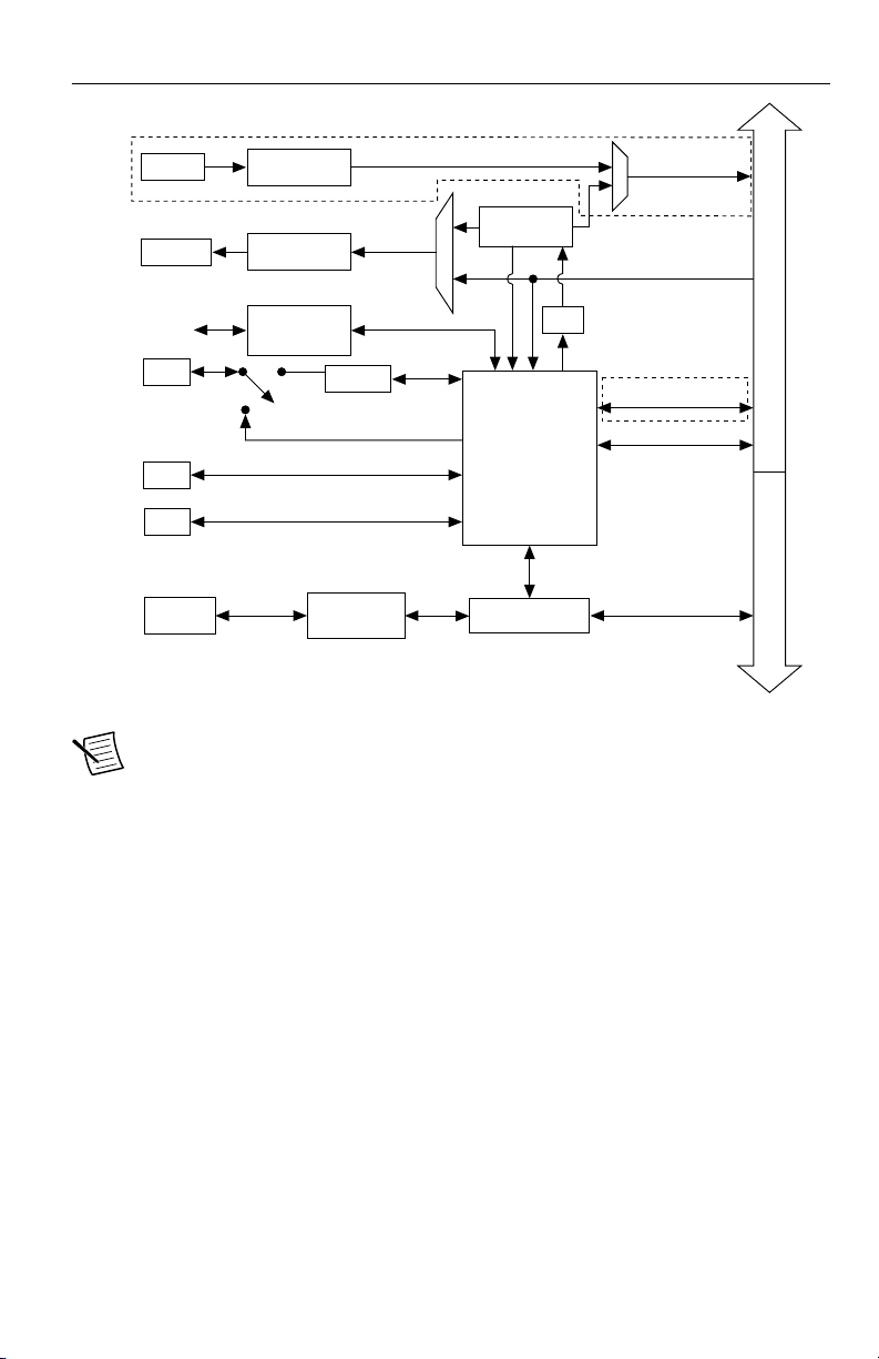
Figure 2. Functional Overview of the PXI-6683
Synchronization
Clock Generation
and
Routing
Circuitry
PCI Interface
PXIPCI
PXI_STAR<0..12>
PXI_TRIG<0..7>
PXI_CLK10_IN
CLKIN
AC Coupled
Clock Detector
PXI_CLK10
PFI 0
IRIG-B AM
Receiver
PFI 1
PFI 2
TCXO
(Oscillator)
CLKOUT
AC Coupling
GPS RF IN
+5 V DC OUT
GPS
Receiver
PFI0 Digital
Ethernet
Controller
Ethernet
Port
Not in NI PXI-6683H
Not in NI PXI-6683H
DAC
Note The PXI-6683H does not have PXI_STAR trigger lines, shown as
PXI_STAR<0..12> in Figure 2. on page 8. The PXI-6683H does not have the
CLKIN circuitry, or the ability to drive PXI_CLK10_IN.
8 | ni.com | PXI-6683(H) User Manual
Page 9

PXI-6683 Front Panel and LEDs
8
9
10
7
6
1
2
3
4
5
Figure 3. PXI-6683 Front Panel
1. GPS LED
2. 1588/802.1AS LED
3. GPS Antenna Connector
4. CLKOUT Connector
5. CLKIN Connector
6. PFI0/IRIG-B Input Connector
7. PFI<1..2> Connectors
8. Ethernet Speed LED
9. Ethernet ACT/LINK LED
10. RJ-45 Ethernet Connector
The GPS LED indicates the status of the GPS hardware.
PXI-6683(H) User Manual
| © National Instruments | 9
Page 10

Table 2. GPS LED Color Description
Color Status
Off Not using GPS*
Amber Attempting to start self survey
Blinking Amber Self survey in progress
Blinking Green Self survey complete (normal operation)
Red Error
†
*The GPS LED is turned off if GPS is not set as the time reference.
†
An error is generated when the antenna is disconnected, when there is an antenna
malfunction, or when there is a hardware malfunction.
The 1588/802.1AS LED indicates the status of the IEEE 1588 or 802.1AS synchronization
protocol.
Table 3. 1588/802.1AS LED Color Description
Color Status
Off Not using 1588 or 802.1AS*
Amber Initializing
Blinking Amber (2 seconds) Listening or Passive
Green Uncalibrated or Slave
Blinking Green (2 seconds) Master or Premaster
Red Faulty
*1588 and/or 802.1AS has been disabled or stopped.
The Ethernet Speed LED indicates the PXI-6683 Series Ethernet link speed.
Table 4. Ethernet Speed LED Description
Color Status
Off 10 Mbps
Green 100 Mbps
Amber 1000 Mbps
10 | ni.com | PXI-6683(H) User Manual
Page 11

The Ethernet ACT/LINK LED indicates the PXI-6683 Series Ethernet link condition.
Table 5. Ethernet ACT/LINK LED
Color Status
Off No Ethernet link
Green Ethernet link established
Blink Ethernet activity occurring
Connectors
This section describes the connectors on the front panel of the PXI-6683 Series. Refer to
Figure 3. on page 9 for the location of the connectors.
• GPS ANT—GPS antenna RF input and DC power output for the active GPS antenna.
This connector provides 5 VDC for an active antenna. This connector also serves as the
input for the RF signal coming in from the GPS antenna.
• CLKOUT—Clock Output. This connector is used to source a 10 MHz clock that can be
routed programmatically from the temperature-compensated crystal oscillator (TCXO) or
backplane clock (PXI_CLK10).
• CLKIN—Clock Input. This connector supplies the module with a clock that can be
programmatically routed to the PXI backplane (PXI_CLK10_IN) for distribution to the
other modules in the chassis when the PXI-6683 is installed in the system timing slot.
Note The PXI-6683H does not have the CLKIN connector.
• PFI<0..2>—Programmable Function Interface <0..2>. These connectors can be used for
either input or output. You can program the behavior of these PFI connections
individually. Additionally, PFI0 can function as an input for IRIG-B DC or AM.
Caution Do not connect an AM signal to PFI0 when the PFI line is
configured for digital operations. This could cause damage to the digital
circuitry, the device driving the AM signal, or both. Always ensure the line is
configured for IRIG-B AM operation before connecting an IRIG-B AM signal.
• RJ-45 Ethernet—10/100/1000 Mbit Ethernet connection. This connector allows the
module to communicate via standard Ethernet cabling.
Caution Connections that exceed any of the maximum ratings of input or
output signals on the PXI-6683 Series can damage the module, the computer, or
other devices connected to the PXI-6683 Series. National Instruments is not
liable for any damage resulting from such signal connections.
Hardware Features
The PXI-6683 Series performs the following functions:
• Synchronization using GPS, IRIG-B, PPS, IEEE 1588, or IEEE 802.1AS.
• Generation of future time events and clock signals, based on the synchronized time.
• Timestamping incoming signals with the synchronized time.
PXI-6683(H) User Manual
| © National Instruments | 11
Page 12

• Routing internally or externally generated signals from one location to another.
• Single-board clock disciplining capability.
[table] outlines the function and direction of the signals discussed in detail in the remainder of
this section. These signals are also identified in Figure 2. on page 8.
Table 6. PXI-6683 Series I/O Terminals
Signal Name Direction Description
PXI_CLK10_IN
(System Timing Slot
only )
(Not in the PXI-6683H)
Out This is a signal that can replace the native 10 MHz
oscillator on the PXI backplane. PXI_CLK10_IN may
originate from the onboard TCXO or from an external
source connected to CLKIN.
PXI_CLK10 In This signal is the PXI 10 MHz backplane clock. By
default, this signal is the output of the native 10 MHz
oscillator in the chassis. A PXI-6683 Series in the
system timing slot can replace this signal with
PXI_CLK10_IN.
Oscillator N/A This is the output of the 10 MHz TCXO. It is used by
the FPGA for synchronization. A PXI-6683 in the
system timing slot can be routed to CLKOUT or
PXI_CLK10_IN. The TCXO is a very stable and
accurate frequency source.
CLKIN
(Not in the PXI-6683H)
In CLKIN is a signal connected to the SMB input pin of
the same name. A PXI-6683 in the system timing slot
can route CLKIN to PXI_CLK10_IN.
CLKOUT Out CLKOUT is the signal on the SMB input pin of the
same name. Either the oscillator (TCXO) or
PXI_CLK10 may be routed to this output.
PXI_STAR<0..12>
(Not in the PXI-6683H)
In/Out The PXI star trigger bus connects the system timing
slot to Slot<3..15> in a star configuration. The
electrical paths of each star line are closely matched to
minimize intermodule skew. A PXI-6683 in the system
timing slot can route signals to Slots<3..15> using the
star trigger bus.
12 | ni.com | PXI-6683(H) User Manual
Page 13

Table 6. PXI-6683 Series I/O Terminals (Continued)
Signal Name Direction Description
PFI<0..2> In/Out The Programmable Function Interface (PFI) pins on the
PXI-6683 Series route timing and triggering signals
between multiple PXI chassis. A wide variety of input
and output signals can be routed to or from the PFI
lines.
PFI<0> can also function as an input for IRIG-B DC or
AM.
PXI_TRIG<0..7> In/Out The PXI trigger bus consists of eight digital lines
shared among all slots in the PXI chassis. The
PXI-6683 Series can route a wide variety of signals to
and from these lines.
The remainder of this section describes how these signals are used, acquired, and generated by
the PXI-6683 Series hardware, and explains how you can use the signals between various
locations to synchronize events in your system.
Clock and Event Generation
The PXI-6683 Series can generate two types of clock signals. The first type is generated with
a precise 10 MHz oscillator, and the second is generated with the synchronized timebase. The
following sections describe the two types of clock generation and explain the considerations
for choosing either type. In addition to time-synchronized clock signals, the PXI-6683 Series
is also capable of generating arbitrary digital events, to be used as triggers.
TCXO, PXI_CLK10, and Clock Disciplining
The PXI-6683 Series features a precision 10 MHz TCXO. The frequency accuracy and
stability of this clock is greater than the frequency accuracy and stability of the native 10 MHz
PXI backplane clock (PXI_CLK10).
The main source of error in most frequency reference oscillators is temperature variation. The
TCXO contains circuitry to measure the temperature of the oscillator and adjust the oscillator's
control voltage to compensate for temperature variations according to the crystal's known
frequency variation across its operating temperature range.
A PXI-6683 module in the system timing slot of a PXI chassis can replace the native PXI 10
MHz backplane frequency reference clock (PXI_CLK10) with the more stable and accurate
output of the TCXO. All other PXI modules in the chassis that reference the 10 MHz
backplane clock benefit from this improved reference. The TCXO does not automatically
replace the native 10 MHz clock; this feature must be explicitly enabled in software. The
TCXO output can also be routed out to the CLKOUT connector.
The PXI-6683 has the capability to discipline its 10 MHz TCXO to an external time reference
(such as GPS, IEEE 1588, or IRIG-B) by monitoring and adjusting the clock relative to the
external time reference. The driver software automatically disciplines the TCXO to the
PXI-6683(H) User Manual
| © National Instruments | 13
Page 14

selected time reference. TCXO disciplining can be disabled by setting the time reference to
Free Running.
Note Some chassis (including the PXI-103x series) require toggling a hardware
switch to enable the system timing module to override PXI_CLK10. Refer to your
chassis user manual for more information.
Time-Synchronized Clock and Event Generation
The PXI-6683 Series is capable of generating clock signals and triggers based on the
synchronized time base. The PXI-6683 Series keeps an internal time base with 10 ns
resolution that can be free running or synchronized to GPS, IEEE 1588, IEEE 802.1AS, IRIGB, or PPS. The NI-Sync API allows you to schedule triggers to occur at an arbitrary future
time (future time events) or clock with high and low times that are multiples of 10 ns (refer to
the PXI-6683 Series Specifications for information about limitations). It is also possible to
program the start and end time of a clock generated in this way.
Refer to Table 7. on page 16 for a list of destinations for synchronized time clocks and future
time events.
PXI_CLK10 Synchronization Design Recommendations
• Minimize Starting and Stopping of PXI_CLK10 Disciplining—From startup, the
PXI_CLK10 synchronization can take on the order of minutes to stabilize to the time
reference. You should design your application such that PXI10 disciplining runs
asynchronous to other programs that might start and stop more frequently. This
minimizes the time spend letting the synchronization stabilize and lock.
• Avoid Disrupting PXI_CLK10 Disciplining—While you can use the devices used for
PXI_CLK10 disciplining within other applications, you should avoid resetting them or
changing the configured time reference. Doing so disrupts the PXI_CLK10 disciplining
process.
Routing Signals
The PXI-6683 Series has versatile trigger routing capabilities. It can route signals to and from
the front panel, the PXI star triggers, and the PXI triggers. In addition, the polarity of the
destination signal can be inverted, which is useful when handling active-low digital signals.
The PXI-6683 Series can replace the PXI backplane's native 10 MHz clock (PXI_CLK10)
with its high-stability TCXO, or with a 10 MHz clock signal from the CLKIN connector. The
PXI-6683 Series can route the TCXO or PXI 10 MHz reference clock to CLKOUT.
Note Replacing PXI_CLK10 is not supported by the PXI-6683H.
Figure 4. on page 15 summarizes the routing features of the PXI-6683 Series.
| ni.com | PXI-6683(H) User Manual
14
Page 15

Figure 4. High-Level Schematic of PXI-6683 Signal Routing Architecture
PXI_Trig 0
PXI_Trig 7
PXI_Star 0
PXI_Star 12
Router for each I/O
PFI 0
PFI 2
PXI_Trig 0
PXI_Trig 7
PXI_Star 0
PXI_Star 12
GND
Clk10
Synchronizer
TCXO
ClkIn
ClkOut
PXI_Clk10_In
PXI_Clk10
PFI 0
PFI 2
PXI_Clk10
Not in NI PXI-6683H
Not in NI PXI-6683H
Not in
NI PXI-6683H
Note The PXI-6683H architecture is identical to the architecture described in the
previous figure, except the PXI-6683H does not have PXI_STAR trigger lines,
CLKIN, or PXI_CLK10_IN.
Determining Sources and Destinations
All signal routing operations can be characterized by a source (input) and a destination. In
addition, synchronous routing operations must also define a third signal known as the
synchronization clock. Refer to the Choosing the Type of Routing section for more information
on synchronous versus asynchronous routing.
Table 7. on page 16 summarizes the sources and destinations of the PXI-6683 Series. The
destinations are listed in the horizontal heading row, and the sources are listed in the column at
the far left. A check in a cell indicates that the source and destination combination defined by
that cell is a valid routing combination.
PXI-6683(H) User Manual
| © National Instruments | 15
Page 16

Table 7. Sources and Destinations for PXI-6683 Series Signal Routing Operations
Destinations
Front Panel Backplane
CLKOUT PFI<0..2> PXI_CLK10_IN* PXI_Star
Front Panel
Sources
*The PXI-6683H does not have a CLKIN connector, PXI_CLK10_IN, or PXI_STAR trigger lines.
†
automatically in most chassis), and then routing PXI_CLK10 to the destination. The source must be 10 MHz.
‡
details.
Backplane
Onboard
Can be accomplished in two stages by routing source to PXI_CLK10_IN, replacing PXI_CLK10 with PXI_CLK10_IN (occurs
Asynchronous routes between a single source and multiple destinations are very low skew. See the PXI-6683(H) Specifications for
CLKIN* X
PFI<0..2> X X
PXI_CLK10 X X X X
PXI_STAR<0..12>* X
PXI TRIG<0..7> X X X
TCXO X X
Time-synchronized
events and clocks
†
†
X
‡
†
X X X
X X
X X
Trigger
<0..12>*
X X
PXI
TRIG
<0..7>
†
‡
†
†
X
X
†
X
I/O Considerations
Using the Ethernet Port
The PXI-6683 Series provides on standard RJ-45 connection for Ethernet communication.
This port auto negotiates to the best possible speed—10 Mbps, 100 Mbps, or 1000 Mbps
(auto-negotiation can be disabled by software). The Ethernet port is auto-MDI capable, which
means crossover cabling is not necessary when connecting the PXI-6683 Series to another
network card. The PXI-6683 Series senses whether a crossed connection is needed and
performs the action internally. The Ethernet port also allows for full duplex operation, so
traffic can be sent and received at the same time.
Using Front Panel PFI Terminals as Outputs
The front panel PFI output signals use +3.3 V signaling for high-impedance loads. You can
use the PFI terminals to generate future time events and clock signals up to 1.5 MHz. PFI
output signals are suitable for driving most LEDs. To ensure proper signal integrity, use cables
with 50 Ω loads, although logic-high voltage will be lower than 3.3 V. Refer to the
PXI-6683(H) specifications for more information. Refer to NI-Sync for information on how to
set up the PFI lines for output.
Caution Do not attempt to drive signals into PFI terminals set up as outputs.
Doing so can damage the PXI-6683 Series or the device driving the PFI terminal.
16 | ni.com | PXI-6683(H) User Manual
Page 17

The signal source for each PFI trigger line configured as an output can be independently
selected from one of the following options:
• Another PFI<0..2>
• PXI_TRIG<0..7>
• PXI_STAR<0..12> (PXI-6683 only)
• Future time events
• PXI_CLK10
• Ground
Tip Invert Ground to get a logic high.
The PFI trigger outputs may be synchronized to CLK10 except when routing future time
events. Refer to the Choosing the Type of Routing section for more information about the
synchronization clock.
Using Front Panel PFI Terminals as Inputs
The front panel PFI terminals can be configured by software to accept input signals. Refer to
the NI-Sync documentation for information on how to set up the PFI terminals to accept input
signals. You can use these terminals to timestamp triggers with the synchronized system time
or to route signals to other destinations (refer to Table 7. on page 16). The input terminals
accept native +3.3 V signaling, but are +5 tolerant. Use 50 Ω source termination when driving
signals into PFI terminals.
The voltage thresholds for the front panel PFI input signals are fixed. Refer to the PXI-6683
Series Specifications for the voltage thresholds. The front panel PFI input signals can be
timestamped on rising, falling, or both edges of an input signal.
PFI0 and SSR Switching
Since PFI0 is a dual-purpose terminal capable of performing digital I/O like the other PFI lines
while also being capable of receiving IRIG-B AM and DC inputs, care is taken to protect the
digital circuitry when PFI0 is being used as an IRIG-B AM input. This is achieved with a
normally-open solid-state relay (SSR), which is closed only when digital operations for the
line are enabled through the API. Digital operations include setting up routes in which PFI0 is
the source or the destination, enabling timestamping for PFI0, scheduling future time events or
clocks for PFI0, and setting IRIG-B DC as the time reference.
The SSR has a 5 ms open and close time. Therefore, care must be taken when using PFI0 to
ensure correct operation when the SSR is switching.
To avoid issues due to the SSR switching, follow these guidelines:
• Whenever timestamping begins on PFI0, either ensure the input will remain at a logic
low state for at least 5 ms or disregard timestamps for at least 5 ms.
• When setting up PFI0 as an output (future time events or clocks), ensure that PFI0 is
driven low for at least 5 ms after the line is set up. Alternately, ensure that the external
receiver can tolerate a slow rising edge.
PXI-6683(H) User Manual
| © National Instruments | 17
Page 18

• Before disabling PFI0 set up as an output, drive the output low to avoid a very slow ramp
Star Trigger Bus
System
Conrtroller
Star Trigger
Controller (Slot 2)
Module
Module
Module
132 Mbytes/s, 33 MHz, 32-bit PCI Bus
PXI Trigger Bus (8 lines)
10 MHz
Clock
down.
• Any time a route is set up or changed where PFI0 is the source or the destination, allow
for a 5 ms settling time.
For more information, refer to KnowledgeBase 4E9BT88P at ni.com/support.
Brief Overview of PXI Synchronization Features
PCI eXtensions for Instrumentation (PXI) is a rugged PC-based platform that offers a highperformance, low-cost deployment solution for measurement and automation systems. PXI
combines the Peripheral Component Interconnect (PCI) electrical bus with the rugged,
modular Eurocard mechanical packaging of CompactPCI and adds specialized
synchronization buses and key software features.
Figure 5. on page 18 provides an overview of the PXI synchronization architecture:
Figure 5. PXI Synchronization Architecture
The PXI trigger bus, PXI star triggers, and PXI_CLK10 are PXI features that enhance
synchronization. The PXI trigger bus is a multi-drop 8-line bus that goes to every slot. The
PXI star trigger bus is a set of up to 13 point-to-point matched-length connections between the
system timing slot and every slot starting with slot 3 and up to slot 15. The propagation delay
between the system timing slot and each destination slot is matched to within 1ns to achieve
low-skew triggering. PXI_CLK10 is a high quality 10 MHz clock that is distributed with low
skew to each PXI slot. This 10 MHz signal can be sourced from the native PXI backplane
oscillator or from the system timing slot controller module installed in the system timing slot
(such as the PXI-6683).
| ni.com | PXI-6683(H) User Manual
18
Page 19

Using the PXI Triggers
The PXI trigger bus is a set of 8 electrical lines that go to every slot in a segment of a PXI
chassis (multi-drop up to 8 slots). Only one PXI module should drive a particular PXI_Trigger
line at a given time. The signal is then received by modules in all other PXI slots. This feature
makes the PXI triggers convenient in situations where you want, for instance, to trigger
several devices, because all modules will receive the same trigger.
Given the architecture of the PXI trigger bus, triggering signals do not reach each slot at
precisely the same time. A difference of several nanoseconds can occur between slots,
especially in larger PXI chassis (which can have buffers between segments). This delay is not
a problem for many applications. However, if your application requires tighter
synchronization, use the PXI_STAR triggers, or use the PXI rigger bus synchronous to
PXI_CLK10.
The multi-drop nature of the PXI trigger bus can introduce signal integrity issues. Therefore,
National Instruments does not recommend the use of PXI_Trigger lines for clock distribution.
The preferred method for clock distribution is the use of the PXI_STAR triggers. However, the
PXI-6683 Series does support routing of clocks to the PXI_Trigger lines, in case you must use
them.
For each PXI_Trigger line configured as an output in the PXI-6683 Series, the signal source
can be independently selected from the following options:
• PFI<0..2>
• Another PXI trigger line (PXI_TRIG<0..7>)
• PXI_STAR<0..12>
• Future time events
• PXI_CLK10
• Ground
Tip Invert Ground to get a logic high.
The PXI trigger outputs may be synchronized to CLK10 except when routing future time
events. Refer to the Choosing the Type of Routing section for more information about the
synchronization clock.
Using the PXI Star Triggers (PXI-6683 Only)
There are up to 13 PXI star triggers per chassis. Each trigger line is a dedicated connection
between the system timing slot and one other slot. The PXI Specification, Revision 2.1,
requires that the propagation delay along each star trigger line be matched to within 1 ns. A
typical upper limit for the skew in most NI PXI chassis is 500 ps. The low skew of the PXI
star trigger bus is useful for applications that require triggers to arrive at several modules
nearly simultaneously. The PXI-6683 is able to route low skew triggers to the PXI_Star lines
from any PFI line.
The star trigger lines are bidirectional, so signals can be sent to the system timing slot from a
module in another slot or from the system timing slot to the other module.
PXI-6683(H) User Manual
| © National Instruments | 19
Page 20

The signal source for each PXI star trigger line configured as an output can be independently
Trigger Input
Trigger Output
Propagation Delay
t
pd
selected from one of the following options:
• PFI<0..2> (low skew)
• PXI_TRIG<0..7>
• Another PXI star trigger line (PXI_STAR<0..12>)
• Synchronized time event
• PXI_CLK10
• Ground
Tip Invert Ground to get a logic high.
The PXI star trigger outputs may be synchronized to CLK10 except when routing future time
events. Refer to the Choosing the Type of Routing section for more information about the
synchronization clock.
Choosing the Type of Routing
The PXI-6683 Series routes signals in one of two ways: asynchronously or synchronously. The
following sections describe the two routing types and the considerations for choosing each
type.
Asynchronous Routing
Asynchronous routing is the most straightforward method of routing signals. Any
asynchronous route can be defined in terms of two signals: a source and a destination. A
digital pulse or train comes in on the source and is propagated to the destination. When the
source signal goes from low to high, this rising edge is transferred to the destination after a
propagation delay through the module. Figure 6. on page 20 illustrates an asynchronous
routing operation.
Figure 6. Asynchronous Routing Operation
Some delay is always associated with an asynchronous route, and this delay varies among
PXI-6683 Series modules, depending on variations in temperature and chassis voltage. Typical
delay times in the PXI-6683 Series for asynchronous routes between various sources and
destinations are given in the device's Specifications.
| ni.com | PXI-6683(H) User Manual
20
Page 21

Asynchronous routing works well if the total system delays are not too long for the
application. Propagation delay could be caused by the following reasons:
• Output delay on the source.
• Propagation delay of the signal across the backplane(s) and cable(s).
• Propagation delay of the signal through the PXI-6683 Series.
• Time for the receiver to recognize the signal.
The source of an asynchronous routing operation on the PXI-6683 Series can be any of the
following lines:
• Any front panel PFI pin (PFI<0..2>)
• Any PXI Star trigger line (PXI_STAR<0..12>) (PXI-6683 only)
• Any PXI trigger line (PXI_TRIG<0..7>)
• Synchronized time events
• PXI_CLK10
• Ground
Tip Invert Ground to get a logic high.
The destination of an asynchronous routing operation on the PXI-6683 Series can be any of
the following lines:
• Any front panel PFI pin (PFI<0..2>)
• Any PXI star trigger line (PXI_STAR<0..12>) (PXI-6683 only)
• Any PXI trigger line (PXI_TRIG<0..7>)
Synchronous Routing
A synchronous routing operation is defined in terms of three signals: a source, a destination,
and a synchronization clock. Unlike asynchronous routing, the output of a synchronous routing
operation does not directly follow the input after a propagation delay. Instead, the logic state
of the input is sampled on each active edge of the synchronization clock, and the output is set
to that logic state after a small delay, as shown in Figure 7. on page 22. Thus, the output is
said to be synchronous with this clock.
Figure 7. on page 22 shows a timing diagram that illustrates synchronous routing.
PXI-6683(H) User Manual
| © National Instruments | 21
Page 22

Figure 7. Synchronous Routing Operation
Trigger Input
Synchronization
Clock
Trigger Output
Setup
Time
t
setup
Hold
Time
t
hold
Clock to Output
Time, t
CtoQ
PXI_CLK10
Trigger@Destination 2
Trigger@Destination 1
Trigger Out@Source
Trigger Synchronously Received
@Destinations 1 and 2
A
B
A: Propagation delay from source to destination 1.
B: Propagation delay from source to destination 2.
The PXI-6683 Series supports synchronous routing to either the rising or falling edge of the
synchronization clock. In addition, the polarity of the destination signal can be inverted, which
is useful when handling active-low digital signals. Synchronous routing can be useful for
eliminating skew when sending triggers to several destinations. For example, when sending
triggers using the PXI Trigger lines, the trigger arrives at each slot at a slightly different time.
However, if the trigger is sent and received synchronously using a low-skew synchronization
clock (for example, PXI_CLK10), all receiving devices can act on the trigger at the same time,
as shown in Figure 8. on page 22:
Figure 8. Synchronous Routing to Multiple Destinations
Synchronous routing requires the input to be stable at a logic low or logic high state with a
window of time around the clock edge. This window of time around the clock edge is defined
by the setup time (t
of time, it is undetermined whether the output of the synchronous route will go to the old or
new logic state. This is important, for example, if a source is being routed synchronously to
| ni.com | PXI-6683(H) User Manual
22
) and hold time (t
setup
). If the input signal changes within this window
hold
Page 23

several destinations. If the source signal changes within the setup-and-hold window around the
Synchronization CLK
Trigger Output 2
Trigger Ouput 1
Trigger Input
t
setup
t
hold
t
CtoQ
t
CtoQ
synchronization clock dge, one of the destinations might go to the new logic level while the
other destination might remain at the old logic level and change when the next synchronization
clock edge occurs, as shown in Figure 9. on page 23:
Figure 9. Synchronous Routing Uncertainty with Setup-and-Hold Variations
Therefore, if your application requires that the trigger arrive at the multiple destinations
simultaneously, you must ensure that the input is stable within the setup and hold window
around the synchronization clock edge. For more information and possible methods to ensure
this requirement is met, go to ni.com/info and enter the Info Code
SyncTriggerRouting.
Possible sources for synchronous routing with the PXI-6683 Series include the following
sources:
• Any front panel PFI pin. (PFI<0..2>)
• Any PXI star trigger line (PXI_STAR<0..12>) (PXI-6683 only)
• Any PXI trigger line (PXI_TRIG<0..7>)
In the PXI-6683 Series, the synchronization clock for synchronous routes is always
PXI_CLK10.
The destination of a synchronous routing operation on the PXI-6683 Series can be any of the
following lines:
• Any front panel PFI pin (PFI<0..2>)
• Any PXI star trigger line (PXI_STAR<0..12>) (PXI-6683 only)
• Any PXI trigger line (PXI_TRIG<0..7>)
Note The possible destinations for a synchronous route are identical to those for an
asynchronous route.
Synchronization
The PXI-6683 Series is capable of achieving tight synchronization with various other devices
using GPS, IRIG-B, PPS, IEEE 802.1AS, or IEEE 1588. When GPS or IRIG-B are selected as
the synchronization source, the PXI-6683 Series module can also serve as an IEEE 1588
grandmaster. The following sections describe the synchronization capabilities of the PXI-6683
Series.
PXI-6683(H) User Manual
| © National Instruments | 23
Page 24

GPS
GPS stands for Global Positioning System, and it is a system of over two dozen satellites in
medium Earth orbit that are constantly transmitting signals down to Earth. GPS receivers are
able to detect these signals and determine location, speed, direction, and time very precisely.
GPS satellites are fitted with atomic clocks, and the signals they transmit to Earth contain
timing information. This makes the GPS system a precise timing and synchronization source.
The PXI-6683 Series has a GPS receiver which powers an active GPS antenna and receives
and processes the RF signals (1.575 GHz) from the satellites. The GPS receiver then generates
a very precise pulse-per-second (PPS) signal that the PXI-6683 Series uses to achieve submicrosecond synchronization.
GPS enables the PXI-6683 Series to synchronize PXI systems located far away from each
other, as long as GPS satellites are visible to the antenna from each location. Furthermore,
once the PXI-6683 Series is synchronized to GPS, it can function as an IEEE 1588
grandmaster to enable synchronization of external 1588 devices.
IRIG-B
IRIG is a standard used to transmit precise timing information between instruments to achieve
synchronization. IRIG-B is a particular application of the IRIG standard, in which 100 bits of
data are sent every second. Embedded in the data is a seconds' boundary marker that the
receiving instrument uses to synchronize its timebase to the IRIG source. The rest of the data
contains information such as the time of day, days since the beginning of the year, and
optionally, control functions and the number of seconds since the start of the day, encoded as a
straight binary number.
The PXI-6683 Series can function as an IRIG-B receiver, supporting synchronization to
sources outputting IRIG-B 12X (AM) and IRIG-B 00X (DC), compliant with the IRIG 200-04
standard.
When configured to synchronize to an IRIG-B AM source, the PXI-6683 Series will be able to
accept a 1 kHz AM modulated IRIG-B 12X signal on its PFI0 input. When configured to
synchronize to an IRIG-B DC source, the PXI-6683 Series will be able to accept an IRIG-B
00X DC encoded signal on its PFI0 input.
Caution Do not connect an AM signal to PFI0 when the PFI line is configured for
digital operations. This could cause damage to the digital circuitry, the device
driving the AM signal, or both. Always ensure the line is configured for IRIG-B AM
operation before connecting an IRIG-B AM signal.
Furthermore, once the PXI-6683 Series is synchronized to IRIG-B, it can function as an IEEE
1588 grandmaster to synchronize external 1588 devices.
The following assumptions are made regarding the received IRIG-B signal. All conditions
must be met for the PXI-6683 Series to be able synchronize accurately:
• Seconds begin every minute at 0, increment to 59, and then roll over to 0.
• Minutes begin every hour at 0, increment to 59, and then roll over to 0.
| ni.com | PXI-6683(H) User Manual
24
Page 25

• Hours begin every day at 0, increment to 23, and then roll over to 0.
• Days begin every year at 1. Days increment to 365 in non-leap years, or to 366 in leap
years, and then roll over to 1. Leap years must be supported. Valid values for year are 01
to 99, inclusive. Years are assumed to be in the 21st century. For instance, year 19
represents 2019. If the year is not supplied (sent as 00), the OS system time is read and
the year is derived from it.
To achieve proper synchronization of the PXI-6683 Series, ensure that the IRIG-B source used
conforms to the requirements listed above. Note that most IRIG-B sources conform to these
requirements.
802.1AS
The IEEE 802.1AS generalized precision time protocol (gPTP) is a standard based on IEEE
1588 that is better optimized for time-sensitive applications. Like 1588, 802.1AS controls
synchronization across a series of nodes connected by Ethernet cables, switches, and bridges
by automatically designating a grandmaster clock using the Best Master Clock algorithm
(BMCA). The grandmaster clock then serves as the source of time to slave devices (devices
not elected as the 1588 grandmaster) across the network.
Each distributed device runs the BMCA to determine the highest ranking, most accurate
device on the network, which automatically becomes the grandmaster. If the grandmaster
clock leaves the network or is no longer the most accurate clock on the network, the BMCA
selects a new grandmaster. The BMCA defines a standard set of clock characteristics—such as
the origin of a clock's time source and the stability of the clock's frequency—and then assigns
a value to each clock in order to determine the grandmaster. The BMCA also takes into
account user-defined priority values, which you can set using the NI-Sync driver software.
One of the main differences between 802.1AS and 1588 is that 802.1AS requires 802.1AScapable network switches and network interfaces providing hardware-assisted timestamping in
order to operate. You can determine whether or not a device is capable of running 802.1AS
using the AS Capable property, accessible with NI-Sync.
IEEE 1588
The PXI-6683 Series is capable of performing synchronization over Ethernet using IEEE
1588. It is possible to configure the PXI-6683 Series to synchronize to GPS or IRIG-B and
then function as an IEEE 1588 grandmaster. It is also possible to configure the PXI-6683
Series to synchronize to IEEE 1588, in which case, the standard defines how the master will
be selected. If the PXI-6683 Series is selected as the IEEE 1588 master, and it is not
configured to synchronize to GPS or IRIG-B, it will use its internal free-running timebase,
which will be updated to the host computer's system time during power up.
Pulse Per Second (PPS)
The PXI-6683 Series is capable of using a PPS signal for synchronization. Any PFI,
PXI_Trigger, or PXI_Star line can be configured as the PPS input terminal. When
synchronizing based on a PPS, the first pulse received will set the PXI-6683 Series internal
timebase to either an arbitrary time supplied by the user, or the host computer's system time.
Each subsequent pulse received will be interpreted as a second's boundary (the pulse occurring
PXI-6683(H) User Manual
| © National Instruments | 25
Page 26

exactly one second after the previous pulse). As each pulse is recieved, the PXI-6683 Series
will adjust its internal timebase to match the frequency of the PPS source.
For best results when using a PPS time reference, ensure that the device supplying the PPS
signal is capable of providing a stable, consistent 1 Hz signal. Error can be induced into the
system if the reference signal contains significant jitter, or if the reference frequency strays
from 1 Hz.
Synchronization Best Practices
The PXI-6683 Series can achieve sub-microsecond synchronization. The following sections
describe some guidelines for achieving the best possible performance from the PXI-6683
Series. While the PXI-6683 Series will function properly if you follow the specifications, the
following guidelines may increase the synchronization performance.
Operating Environment
In order to achieve the best synchronization performance, refer to the following guidelines to
provide a thermally stable environment. Also, ensure you remain within the specified
operating temperature limits:
• Place the PXI or PXI Express chassis containing the PXI-6683 Series module in an
environment free of rapid temperature transitions.
• Ensure that PXI filler panels are properly installed for unused PXI or PXI Express slots,
since consistent airflow can degrade the PXI-6683 Series performance.
• Perform the same steps listed above for any other synchronization partners and/or
systems.
Timing System Performance
The PXI-6683 Series can generate or receive a 1 Hz pulse per second signal on any PFI or PXI
trigger terminal. You can set up this signal to transition on the seconds boundary of the
synchronized system time. You can then use this signal to analyze system performance by
connecting two or more pulse per second signals to an oscilloscope and measuring the latency
between them. Adjustments can be made to account for deterministic latency; refer to NI-Sync
documentation for more information. The PXI-6683 Series can also timestamp an incoming
pulse per second signal. The PXI-6683 Series will timestamp the externally-generated pulse
per second with its internal timebase. By comparing this timestamp with the nearest seconds
boundary, you can quickly determine the synchronization performance.
IEEE 1588 Synchronization Best Practices
Network Topology
To obtain the best PXI-6683 Series performance, follow these guidelines to set up the Ethernet
network topology:
| ni.com | PXI-6683(H) User Manual
26
Page 27

• Use short cabling when possible. Ethernet cabling is inherently asymmetric; the longer
the cabling, the higher the asymmetry. This impacts synchronization performance,
because the IEEE 1588 protocol assumes a symmetrical network path.
• If several 1588 devices need to be synchronized on the same network, use a 1588-enabled
switch. 1588-enabled switches are specifically designed to compensate for the varying
latency of packets passing through them; thus enhancing synchronization performance.
• If a 1588-enabled switch is not available, use hubs when connecting to multiple IEEE
1588devices. Unlike standard switches, hubs offer low latency and close to deterministic
performance for Ethernet traffic. Standard Ethernet switches can have Ethernet packet
latencies vary by hundreds of nanoseconds. This latency uncertainty degrades
synchronization performance significantly.
• Ensure that the network is running at 1 Gbps by noting the Ethernet Speed LED status.
Synchronization performance is degraded when running at 10 or 100 Mbps.
Note If it is impossible to use a 1000 or 100 Mbps network and you must run
IEEE 1588 synchronization using a 10 Mbps network, ensure the network
interface of the PXI-6683 Series is explicitly configured for 10 Mbps full
duplex operation using the Windows configuration panels.
GPS Synchronization Best Practices
The PXI-6683 Series module has one SMB female connector on its front panel for a GPS
active antenna. The connector provides a DC voltage to power the antenna and alos serves as
input for the GPS RF signal.
Antenna Installation
Caution National Instruments recommends using a lightning arrester in line with
the GPS antenna installation to protect the PXI-6683 Series module and the PXI
system from possible damage and operators from injury in the event of lightning.
The embedded GPS receiver in the PXI-6683 Series module requires signals from several
satellites to compute accurate timing and location. The more satellites available to the receiver,
the more accurately it can determine time and location. Therefore, the antenna location should
be such that it receives signals from the greatest number of satellites possible. As the number
of satellites visible to the antenna decreases, the synchronization performance may also
decrease. Choose the antenna location so that the antenna has a clear view of the sky. There is
no strict definition for a clear view of the sky, but a suitable guideline is that the GPS antenna
should have a straight line of sight to the sky in all directions (360°), down to an imaginary
line making a 30° angle with the ground. Locations far from trees and tall buildings that could
block or reflect GPS satellite signals are best.
Maximum Cable Length
Maximum cable length depends on the GPS antenna gain and the cable's loss of per unit of
distance. National Instruments recommends a GPS signal strength of between -135 dBm and
-120 dBm at the PXI-6683 Series module's SMB input. GPS signal strength on the Earth's
PXI-6683(H) User Manual
| © National Instruments | 27
Page 28

surface is typically -130 dBm. Targeting a signal strength of -125 dBm at the SMB input, you
can compute the maximum cable length as:
Max_cable_loss = -130 dBm + antenna_gain - (-125 dBm)
Max_cable_length = Max_cable_loss / (loss_per_unit_of_distance)
For example, if you use an active antenna with gain of 28 dB and RG-58 cable, which has a
rated loss at 1.5 GHz of about 0.8 dB/m (24.5 dB/100 ft), the maximum cable length you
could use is:
Max_cable_loss = -130 dBm + 28 DB - (-125 dBm) = 23 dB
Max_cable_length = 23 dB / (.08 dB/m) ≈ 29 m
Note The GPS antenna kit offered by National Instruments comes with a 30 m
cable, which has a loss of 15 dB/100 ft, making the total loss in the cable
approximately 14.8 dB.
Calibration
This section discusses the calibration of the PXI-6683 and PXI-6683H.
Calibration consists of verifying the measurement accuracy of a device and correcting for any
measurement error. The PXI-6683 Series are factory calibrated before shipment at
approximately 25 °C to the levels indicated in the Specifications. The associated calibration
constants—the corrections that were needed to meet specifications—are stored in the onboard
nonvolatile memory (EEPROM). The driver software uses these stored values.
Factory Calibration
All PXI-6683 Series boards go through factory calibration. During that process the TCXO
frequency is adjusted so that it matches a reference 10 MHz atomic clock. A calibration
constant is then stored in on-board, non-olvatile memory, along with other calibration
metadata, such as calibration date and temperature.
The calibration constant is used at start-up when the board is configured for free running
mode. When the PXI-6683 Series module is configured to use GPS, IEEE 1588, IEEE
802.1AS, IRIG-B, or PPS as its time reference, the TCXO frequency is adjusted according to
the time reference, and the calibration constant is no longer used. If the board returns to free
running mode, because it was so configured or the time reference is no longer present, then the
last applied TCXO voltage is retained (it does not revert to the calibration constant).
Note If the board is configured to use IEEE 1588 as the time reference and is
selected as the 1588 master with 1588's BMCA, the device will be free running and
use its calibration constant.
Additional Information
Refer to ni.com/calibration for additional information on NI calibration services.
| ni.com | PXI-6683(H) User Manual
28
Page 29

Information is subject to change without notice. Refer to the NI Trademarks and Logo Guidelines at ni.com/
trademarks for information on NI trademarks. Other product and company names mentioned herein are trademarks or
trade names of their respective companies. For patents covering NI products/technology, refer to the appropriate
location: Help»Patents in your software, the patents.txt file on your media, or the National Instruments Patent Notice
at ni.com/patents. You can find information about end-user license agreements (EULAs) and third-party legal notices
in the readme file for your NI product. Refer to the Export Compliance Information at ni.com/legal/export-
compliance for the NI global trade compliance policy and how to obtain relevant HTS codes, ECCNs, and other import/
export data. NI MAKES NO EXPRESS OR IMPLIED WARRANTIES AS TO THE ACCURACY OF THE INFORMATION
CONTAINED HEREIN AND SHALL NOT BE LIABLE FOR ANY ERRORS. U.S. Government Customers: The data
contained in this manual was developed at private expense and is subject to the applicable limited rights and restricted
data rights as set forth in FAR 52.227-14, DFAR 252.227-7014, and DFAR 252.227-7015.
© 2013—2019 National Instruments. All rights reserved.
373656C-01 October 2, 2019
 Loading...